EP0786755A2 - Affichage à cristaux liquides avec tension à compensation de température - Google Patents
Affichage à cristaux liquides avec tension à compensation de température Download PDFInfo
- Publication number
- EP0786755A2 EP0786755A2 EP96203676A EP96203676A EP0786755A2 EP 0786755 A2 EP0786755 A2 EP 0786755A2 EP 96203676 A EP96203676 A EP 96203676A EP 96203676 A EP96203676 A EP 96203676A EP 0786755 A2 EP0786755 A2 EP 0786755A2
- Authority
- EP
- European Patent Office
- Prior art keywords
- voltage
- drive voltage
- temperature
- drive
- driver
- Prior art date
- Legal status (The legal status is an assumption and is not a legal conclusion. Google has not performed a legal analysis and makes no representation as to the accuracy of the status listed.)
- Ceased
Links
- 239000004973 liquid crystal related substance Substances 0.000 title claims description 10
- 230000004044 response Effects 0.000 claims description 12
- 238000000034 method Methods 0.000 claims description 8
- 238000004519 manufacturing process Methods 0.000 claims description 7
- 238000004364 calculation method Methods 0.000 claims description 5
- 230000001419 dependent effect Effects 0.000 claims description 4
- 230000002093 peripheral effect Effects 0.000 claims description 4
- 230000003247 decreasing effect Effects 0.000 claims description 2
- 230000003213 activating effect Effects 0.000 claims 1
- 230000036755 cellular response Effects 0.000 abstract 1
- 239000004020 conductor Substances 0.000 description 7
- 238000010586 diagram Methods 0.000 description 3
- 239000000203 mixture Substances 0.000 description 3
- 239000000463 material Substances 0.000 description 2
- 101100532521 Homo sapiens AHCYL1 gene Proteins 0.000 description 1
- 102100022479 S-adenosylhomocysteine hydrolase-like protein 1 Human genes 0.000 description 1
- XUIMIQQOPSSXEZ-UHFFFAOYSA-N Silicon Chemical compound [Si] XUIMIQQOPSSXEZ-UHFFFAOYSA-N 0.000 description 1
- 238000005299 abrasion Methods 0.000 description 1
- 230000005540 biological transmission Effects 0.000 description 1
- 230000002860 competitive effect Effects 0.000 description 1
- 230000007423 decrease Effects 0.000 description 1
- 230000000694 effects Effects 0.000 description 1
- 230000008020 evaporation Effects 0.000 description 1
- 238000001704 evaporation Methods 0.000 description 1
- 238000010438 heat treatment Methods 0.000 description 1
- 238000012886 linear function Methods 0.000 description 1
- 229910052710 silicon Inorganic materials 0.000 description 1
- 239000010703 silicon Substances 0.000 description 1
Images


Classifications
-
- G—PHYSICS
- G09—EDUCATION; CRYPTOGRAPHY; DISPLAY; ADVERTISING; SEALS
- G09G—ARRANGEMENTS OR CIRCUITS FOR CONTROL OF INDICATING DEVICES USING STATIC MEANS TO PRESENT VARIABLE INFORMATION
- G09G3/00—Control arrangements or circuits, of interest only in connection with visual indicators other than cathode-ray tubes
- G09G3/20—Control arrangements or circuits, of interest only in connection with visual indicators other than cathode-ray tubes for presentation of an assembly of a number of characters, e.g. a page, by composing the assembly by combination of individual elements arranged in a matrix no fixed position being assigned to or needed to be assigned to the individual characters or partial characters
- G09G3/34—Control arrangements or circuits, of interest only in connection with visual indicators other than cathode-ray tubes for presentation of an assembly of a number of characters, e.g. a page, by composing the assembly by combination of individual elements arranged in a matrix no fixed position being assigned to or needed to be assigned to the individual characters or partial characters by control of light from an independent source
- G09G3/36—Control arrangements or circuits, of interest only in connection with visual indicators other than cathode-ray tubes for presentation of an assembly of a number of characters, e.g. a page, by composing the assembly by combination of individual elements arranged in a matrix no fixed position being assigned to or needed to be assigned to the individual characters or partial characters by control of light from an independent source using liquid crystals
- G09G3/3611—Control of matrices with row and column drivers
- G09G3/3696—Generation of voltages supplied to electrode drivers
-
- G—PHYSICS
- G09—EDUCATION; CRYPTOGRAPHY; DISPLAY; ADVERTISING; SEALS
- G09G—ARRANGEMENTS OR CIRCUITS FOR CONTROL OF INDICATING DEVICES USING STATIC MEANS TO PRESENT VARIABLE INFORMATION
- G09G2320/00—Control of display operating conditions
- G09G2320/04—Maintaining the quality of display appearance
- G09G2320/041—Temperature compensation
Definitions
- This invention relates to a liquid crystal display (LCD) and particularly to such a display having a temperature compensated drive voltage control.
- LCD liquid crystal display
- Automotive instrument clusters have limited room for displaying messages. With the advent of serial communication links in vehicles and more complex systems which must be monitored, the number of tell-tale warnings which accompany these systems has greatly increased to the point that there is insufficient available area for them. It has been proposed to use a small reconfigurable display which displays one message at a time. If more than one message is called for, a microprocessor will sequence the messages in time. Such a display is subject to a number of constraints. The area taken up in the cluster must be minimal and is not to be substantially larger than a single display area itself. It must operate over a wide temperature range, at least -40°C to +95°C. Further the display must by as inexpensive as possible so that it is competitive. It is desirable that the message area be dead fronted when messages are not displayed.
- a LCD be used for the display.
- Such displays require a driver which typically is an integrated circuit (IC).
- IC integrated circuit
- Most commercial LCD driving ICs are poorly suited for the application and tend to be over designed in some areas and under designed in others.
- the LCD display for this application needs a display format of 14 pixels high by 90 pixels wide or 1260 pixels.
- Commercial LCD driving ICs are tuned for general applications and typically require two or more ICs to obtain the necessary pixel count.
- Commercial driver ICs use general output drivers which are much larger and more expensive than required for this application.
- a small display can accommodate only a limited number of connections between the IC driver and the LCD.
- multiplex rates increase the voltages used to operate the cell have to be controlled more precisely and have to be compensated over the temperature range. Due to the wide temperature range the maximum voltage varies greatly, say, from 6 to 12 volts. To assure correct voltage for every point in the range the temperature of the LCD cell has to be closely monitored, within a degree or so.
- the optimum voltage is also dependent on the liquid crystal material in the cell, and the LCD characteristics can vary from cell to cell or from batch to batch. The voltage must also be compensated for that variation.
- the number of messages which are to be displayed is not generally limited, so that such parts are designed to have each pixel state (1260 in this case) loaded into them by a microprocessor.
- downloading that much data by a microprocessor which is busy with other tasks comprises a severe software burden.
- a tell-tale display there is a limited number of messages which must be displayed (typically 30 or less) and so it becomes possible and desirable to use another technique to avoid the downloading task.
- An IC driver chip is directly mounted on an LCD package such that the driver is at the same temperature as the LCD cell, and is connected to the cell by many conductors of a circuit board to energize rows and columns of the cell. To minimize the number of connections to the cell and thereby minimize the size of the cell, the display is highly multiplexed.
- the IC driver includes a ROM containing a bit-mapped image of every desired message.
- a serial peripheral interface in the IC driver couples the driver to a remote microprocessor which selects the message to be displayed.
- a temperature sensor in the driver is periodically sampled and the microprocessor calculates the compensated voltage and outputs a temperature command.
- a voltage multiplier in the IC driver is controlled by the command to produce the desired voltage. Another factor in calculating the optimum voltage is the nature of the liquid crystal composition which may vary from cell to cell. In manufacture, the cells are tested for response to voltage, sorted into batches, and physically coded according to response characteristics. In use, the code is read by the driver IC and provided via serial communication to the microprocessor which includes that data in the calculation of the compensated voltage.
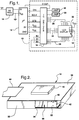
- FIG. 1 shows an LCD package 10 under control of a remotely located microprocessor 12.
- a 5 volt regulator 14 supplied by vehicle ignition voltage couples 5 volts, (V DD ) and ground (V SS ) to the microprocessor. Those voltages in turn are coupled to an IC driver 16 in the LCD package 10.
- the microprocessor also is connected to the IC driver by lines which supply serial data in (DIN), clock (SCLK) and strobe (STB) signals. Data out (DOUT) signals are coupled from the IC driver to the microprocessor.
- the voltage V DD supplied by the regulator is subject to lot variations but upon manufacture of the microprocessor system the voltage is calibrated and the variation is kept in the microprocessor EEPROM so that it can correct the voltage.
- liquid crystal compositions may vary from batch to batch or a composition may vary due to evaporation of some components during cell manufacture, there is some variation in response of cells to a given voltage. It is useful then to grade the cells, preferably upon manufacture, into categories of response. A permanent code is imposed on each LCD cell to designate its category.
- three links 18 on the LCD cell 22 connect the voltage V DD to ports B0, B1 and B2 of the driver. The links are selectively cut by laser, abrasion, or otherwise to establish a 3 bit code which designates the response category.
- Lamps 20 which are preferably LEDs to minimize heating of the LCD cell are turned on and off by signals from the IC driver in response to microprocessor control signals to furnish backlighting of the LCD cell.
- the LCD cell 22 is energized by 14 conductors 24 from row drivers in the IC 16 and two sets 26 of 45 conductors each from upper and lower column drivers in the IC.
- the LCD package 10 includes a housing 30, the LCD cell 22, a circuit board 34 spaced from the cell 22, and elastomeric connectors 36 (one on each side) to connect the circuit board conductors 24 and 26 to the cell 22.
- the conductors emanate from the IC driver chip 16 which is directly attached to the circuit board 34.
- the driver is connected by wire bonding to the conductors.
- Two LEDs (not shown) on the circuit board 34 are held in the space between the circuit board and the cell 22 to backlight the cell.
- a light box 38 comprising a white plastic material has a wall 40 adjacent the circuit board and side walls 42 to efficiently distribute light from the LEDs to the LCD cell.
- a flexible circuit 44 attached to the circuit board 34 has conductors for connecting the IC driver and the remote microprocessor.
- the housing is, for example, 1.75 inches long, 1.35 inches wide, and 0.4 inch deep.
- the display area is 0.625 by 1.2 inches and contains 1260 pixels for a high resolution display image. Due to the chip on board configuration which minimizes thermal mass and the LED lighting which introduces little heat, a temperature sensor in the IC can reliably track the LCD temperature.
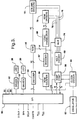
- the IC driver 16 is shown more fully in Figure 3. It includes a serial peripheral interface (SPI) 50 having as inputs the DIN, SCLK and STB signals, supply voltage V DD , and ground V SS , and the output signal DOUT, all carried by the flexible circuit 44. Further, the SPI has inputs for B0, B1 and B2 from the links 18 to pass the digital LCD code to the microprocessor. Two lamp drivers 52 and associated LEDs 20 are connected to SPI outputs.
- a decoder 54 is coupled to the SPI and has 32 output lines connected to a select input of a ROM 56. The ROM stores up to 32 bit-mapped images to be displayed, arranged in a 14 row by 90 column format. The decoder 54 selects one of the images to be displayed.
- a temperature compensation circuit 58 is coupled by an on/off line and 8 line input and output connections to the SPI.
- the compensator 58 measures the LCD package temperature and sends temperature data to the microprocessor via the SPI, and the microprocessor, in turn, sends a voltage command to the compensator which produces that voltage, V LCD .
- the temperature data sent to the microprocessor is independent of the absolute value of V DD , that is, it is ratiometric.
- a voltage divider 60 produces several equally incremented voltages from the compensator output V LCD , i.e. voltages at 100%, 80%, 60%, 40% and 20% of V LCD , and ground.
- An oscillator 62 running at a fixed rate supplies clock pulses via a clock divider 64.
- Circuitry for constructing a display image in accordance with a selected ROM image includes a row counter 66 driven by the clock divider 64 and which is coupled to a decoder 67 which sequentially energizes 14 row address lines which connect to the ROM.
- the row address lines also are fed through a level translator 68 to 14 row drivers 70.
- the ROM has 90 output lines which connect to 90 column drivers 72.
- a multiplexer 74 driven by a row counter output and receiving the several voltages from the divider 60, outputs a pattern of voltage waveforms via lines 76 and 78 to the column drivers and the row drivers to effect the desired state of each display pixel. This is achieved by 14 phase multiplexing through energizing one row at a time. This level of multiplexing requires five voltage levels plus ground from the voltage divider 60 and the voltages have to be accurately compensated to suitably operate the display over a wide range of temperatures and as well as for various LCD characteristics.
- Temperature command input lines DAC0 to DAC7 are coupled to a first set of inputs of a multiplexer 80.
- Inputs to a control logic circuit 82 are two frequency lines carrying 3.9 kHz and 125 kHz from the clock divider 64, a slot 14 line from the row decoder 67 which identifies when the 14th row is activated, a power on reset for initializing the logic, and a comparator output line.
- An up/down counter 84 is also coupled to the reset line and has clock input and an up/down control fed from the logic circuit 82 output.
- the logic circuit also outputs an A/B switch signal to control the multiplexer 80.
- the counter outputs are connected to multiplexer 80 inputs and to latch 86 inputs.
- the latch outputs A/D0 to A/D7 comprise the digital temperature output to the microprocessor via the SPI.
- a latch enable pin LE is connected to the A/B switch line.
- the multiplexer 80 outputs are connected to a digital to analog converter (DAC) 88.
- DAC digital to analog converter
- the resulting analog voltage is coupled to the positive input terminal of a comparator 90.
- the negative input is coupled through a multiplexer 92 to a temperature sensor 94 and to a feedback line 96 of a charge pump 98.
- the comparator 90 output is fed to an AND gate 100 which also has inputs from the on/off line and the A/B switch line.
- a voltage multiplier 102 includes a charge pump 104 excited by an oscillator 106.
- the gate 100 output is connected to enable inputs of both the oscillator and the charge pump.
- the output of the charge pump is connected by a voltage divider 108 to ground to produce a tap output on feedback line 96 which equals 5/11*V LCD .
- the output V LCD is also connected to ground by a FET 110 which is coupled through an inverter 112 to the on/off line so that an off signal causes the FET to conduct thereby grounding the V LCD output.
- the on/off line is turned on to turn off the FET 110, the B phase of the multiplexers 80 and 92 is selected and the AND gate 100 is enabled to enable the charge pump.
- the digital voltage command DAC0 to DAC 7 is input to the DAC 88 which generates an analog command voltage on the input of the comparator 90 which, via the AND gate, causes the charge pump to operate to increase the voltage of the V LCD output until the feedback 96 voltage attains the level of the analog command voltage. At that point the V LCD output is equal to 11/5 times the analog command voltage.
- the temperature sensor 94 comprises an NPN silicon transistor 112 having its collector connected through a resistor 114 to V DD and its emitter connected through a resistor 116 to ground.
- the base is connected via divider resistors 118 and 120 to V DD and ground respectively; the base voltage of the transistor is fixed by the voltage divider 118, 120.
- the base voltage serves to offset the sensor voltage vs. temperature characteristic.
- the resistors 114 and 116 determine the gain of the circuit. In this manner the V BE drop is amplified and offset. For any given current the temperature coefficient of V BE is a very linear function of temperature. As temperature increases, the sensor V BE drop becomes smaller, thus increasing the voltage on the emitter resistor, decreasing the collector voltage. On the other hand, as temperature decreases, the collector voltage increases.
- the logic circuit In operation of the temperature sensor 94, the logic circuit briefly switches the A/B signal to the A phase in the middle of the slot 14 (when row 14 is selected for display). Then the up/down counter 84 is connected by the multiplexer 80 to the DAC 88 to impose a voltage on the comparator 90, and the transistor 112 collector is connected by the multiplexer 92 to the comparator. The DAC and the comparator are then used to implement an analog to digital converter. The comparator output is coupled to the control logic to cause the counter 84 to increment or decrement to change the DAC output to match the temperature sensor output, so that the counter value is the updated temperature data.
- the latch 86 loads the counter contents, and the DAC and comparator are returned to the task of servicing the charge pump.
- the temperature data is serially fed to the microprocessor which calculates the desired voltage and serially transmits a voltage command to the temperature compensation circuit in the IC driver.
- FIG. 5 is a voltage/temperature curve illustrating the variation of operation voltage for a typical LCD cell.
- the cells may have a substantial range of characteristics; they are sorted into perhaps eight groups of similar voltage curves and the curve for each group is specified.
- Each cell is coded according to its group by selectively cutting the links 18 so that the IC driver can read the group code.
- the voltage/temperature curve is embodied in a look-up table in the microprocessor.
- the calibration of the temperature compensation and the compensation method are depicted in flow charts of Figures 6 and 7 wherein the functional description of each block in the chart is accompanied by a number in angle brackets ⁇ nn ⁇ which corresponds to the reference number of the block.
- the calibration procedure is shown in Figure 6.
- the ambient temperature (CALTEMP) is input to the microprocessor and stored in non-volatile memory ⁇ 130 ⁇ .
- the digitized output of the temperature sensor is stored in the same way ⁇ 132 ⁇ .
- the slope of the temperature sensor is a constant stored in the microprocessor program.
- the compensation method shown in Figure 7 requires reading the LCD code ⁇ 134 ⁇ and selecting the look-up table for the voltage curve corresponding to that code ⁇ 136 ⁇ .
- the slope is V DD /255*SS where SS is sensor slope which may be about 20 mv/°C. That gain value SS is predetermined and the initial value of V DD is measured upon manufacture and both are stored in the non-volatile memory.
- the value of SLOPE then is a constant.
- TEMP varies linearly with the difference between the sensor output and its calibration value to produce an offset in the temperature.
- TEMP is used to address the look-up table to find the required operating voltage V LCD ⁇ 142 ⁇ .
- a voltage command value is calculated ⁇ 144 ⁇ such that the voltage multiplier will produce the right voltage.
- the custom IC driver is effective to monitor the temperature of the LCD cell without significantly contributing heat to the cell, and is able to read the LCD code as well. These data are used by the remote microprocessor to determine a voltage command, and a voltage multiplier on the IC chip responds to the command to produce the LCD operating voltage. The net result is that the voltage is accurately controlled over a wide temperature range for a variety of LCD response characteristics so that suitable voltages are available to support a high multiplex rate.
- the ROM in the IC driver stores all the display images to thereby relieve the microprocessor of the image transmission burden.
Landscapes
- Engineering & Computer Science (AREA)
- Chemical & Material Sciences (AREA)
- Crystallography & Structural Chemistry (AREA)
- Physics & Mathematics (AREA)
- Computer Hardware Design (AREA)
- General Physics & Mathematics (AREA)
- Theoretical Computer Science (AREA)
- Liquid Crystal (AREA)
- Liquid Crystal Display Device Control (AREA)
- Control Of Indicators Other Than Cathode Ray Tubes (AREA)
Applications Claiming Priority (2)
| Application Number | Priority Date | Filing Date | Title |
|---|---|---|---|
| US593753 | 1984-03-27 | ||
| US08/593,753 US5936603A (en) | 1996-01-29 | 1996-01-29 | Liquid crystal display with temperature compensated voltage |
Publications (2)
| Publication Number | Publication Date |
|---|---|
| EP0786755A2 true EP0786755A2 (fr) | 1997-07-30 |
| EP0786755A3 EP0786755A3 (fr) | 1997-10-15 |
Family
ID=24376019
Family Applications (1)
| Application Number | Title | Priority Date | Filing Date |
|---|---|---|---|
| EP96203676A Ceased EP0786755A3 (fr) | 1996-01-29 | 1996-12-23 | Affichage à cristaux liquides avec tension à compensation de température |
Country Status (3)
| Country | Link |
|---|---|
| US (1) | US5936603A (fr) |
| EP (1) | EP0786755A3 (fr) |
| JP (1) | JPH09265080A (fr) |
Cited By (3)
| Publication number | Priority date | Publication date | Assignee | Title |
|---|---|---|---|---|
| EP1098292A3 (fr) * | 1999-11-05 | 2002-10-02 | Seiko Epson Corporation | Circuit intégré de commande d'un dispositif électro-optique |
| EP1705637A1 (fr) * | 2005-03-21 | 2006-09-27 | Siemens Aktiengesellschaft | Unité d'affichage pourvue d'un module LCD et de plusieurs pilotes |
| EP1233401A3 (fr) * | 2001-02-14 | 2006-10-11 | Sony Corporation | Projecteur à cristaux liquides et méthode de commande pour un projecteur à cristaux liquides |
Families Citing this family (39)
| Publication number | Priority date | Publication date | Assignee | Title |
|---|---|---|---|---|
| DE69839436D1 (de) * | 1997-03-11 | 2008-06-19 | Nxp Bv | Elektro-optische anzeigevorrichtung |
| WO1999010868A1 (fr) * | 1997-08-26 | 1999-03-04 | Koninklijke Philips Electronics N.V. | Afficheur |
| US6333728B1 (en) * | 1998-09-03 | 2001-12-25 | International Business Machines Corporation | Method and apparatus for real-time on-off contrast ratio optimization in liquid crystal displays |
| JP3539555B2 (ja) * | 1999-10-21 | 2004-07-07 | シャープ株式会社 | 液晶表示装置 |
| TWI234134B (en) * | 2000-04-14 | 2005-06-11 | Koninkl Philips Electronics Nv | Display driver with double calibration means |
| TW495731B (en) * | 2001-02-06 | 2002-07-21 | Winbond Electronics Corp | Reference voltage circuit and method with controllable temperature coefficients |
| JP3664102B2 (ja) * | 2001-06-05 | 2005-06-22 | セイコーエプソン株式会社 | 表示装置及びその信号処理方法 |
| JP2003330419A (ja) * | 2002-05-15 | 2003-11-19 | Semiconductor Energy Lab Co Ltd | 表示装置 |
| US6879111B2 (en) * | 2002-05-29 | 2005-04-12 | Delphi Technologies, Inc. | DC/AC and DC/DC power supply for LCD displays |
| US20050052437A1 (en) * | 2002-08-14 | 2005-03-10 | Elcos Microdisplay Technology, Inc. | Temperature sensor circuit for microdisplays |
| US7385582B2 (en) * | 2002-08-23 | 2008-06-10 | Edwin Lyle Hudson | Temperature control and compensation method for microdisplay systems |
| US20040056989A1 (en) * | 2002-09-24 | 2004-03-25 | Betz Alexander C. | Parameter floodlit LCD |
| US7271790B2 (en) * | 2002-10-11 | 2007-09-18 | Elcos Microdisplay Technology, Inc. | Combined temperature and color-temperature control and compensation method for microdisplay systems |
| KR100546384B1 (ko) * | 2003-09-30 | 2006-01-26 | 삼성전자주식회사 | 현재의 온도를 감지하여 이에 상응하는 디지털 데이터를 출력하는 온도 감지기 |
| CN100458906C (zh) * | 2004-02-20 | 2009-02-04 | 三星电子株式会社 | 脉冲补偿器、显示装置及驱动该显示装置的方法 |
| KR101056374B1 (ko) * | 2004-02-20 | 2011-08-11 | 삼성전자주식회사 | 펄스 보상기, 이를 갖는 영상표시장치 및 영상표시장치의구동방법 |
| US20060007207A1 (en) * | 2004-04-01 | 2006-01-12 | Toshiba Matsushita Display Technology Co., Ltd. | Liquid crystal display device and method of driving liquid crystal display device |
| US7482629B2 (en) * | 2004-05-21 | 2009-01-27 | Semiconductor Energy Laboratory Co., Ltd. | Display device and electronic device |
| US7102121B2 (en) * | 2004-06-29 | 2006-09-05 | Magiq Technologies, Inc. | Temperature compensation for QKD systems |
| JP2006235309A (ja) * | 2005-02-25 | 2006-09-07 | Tohoku Pioneer Corp | 表示パネルの駆動装置及び駆動方法 |
| KR100734311B1 (ko) * | 2006-02-07 | 2007-07-02 | 삼성전자주식회사 | 온도를 보상하여 디스플레이 패널을 구동하는 장치 및 방법 |
| JP4862532B2 (ja) * | 2006-07-26 | 2012-01-25 | 株式会社デンソー | 負荷駆動回路 |
| KR101541443B1 (ko) * | 2007-04-04 | 2015-08-04 | 삼성디스플레이 주식회사 | 액정 표시 장치 |
| WO2009098740A1 (fr) * | 2008-02-06 | 2009-08-13 | Panasonic Corporation | Dispositif d'affichage d'image |
| TWI406502B (zh) * | 2010-12-14 | 2013-08-21 | Au Optronics Corp | 具有自動線性溫度調整功能之閘極驅動電路 |
| JP5080681B1 (ja) * | 2011-11-18 | 2012-11-21 | 株式会社ナナオ | 表示装置、コンピュータプログラム、記録媒体及び温度推定方法 |
| KR102614098B1 (ko) * | 2016-07-26 | 2023-12-13 | 엘지디스플레이 주식회사 | 전압보상회로 및 이를 포함하는 표시장치 |
| US11030942B2 (en) | 2017-10-13 | 2021-06-08 | Jasper Display Corporation | Backplane adaptable to drive emissive pixel arrays of differing pitches |
| US10951875B2 (en) | 2018-07-03 | 2021-03-16 | Raxium, Inc. | Display processing circuitry |
| US11710445B2 (en) | 2019-01-24 | 2023-07-25 | Google Llc | Backplane configurations and operations |
| US11637219B2 (en) | 2019-04-12 | 2023-04-25 | Google Llc | Monolithic integration of different light emitting structures on a same substrate |
| US11238782B2 (en) | 2019-06-28 | 2022-02-01 | Jasper Display Corp. | Backplane for an array of emissive elements |
| US11626062B2 (en) | 2020-02-18 | 2023-04-11 | Google Llc | System and method for modulating an array of emissive elements |
| JP7581367B2 (ja) | 2020-04-06 | 2024-11-12 | グーグル エルエルシー | バックプレーン及びディスプレイアセンブリ |
| US12573349B2 (en) | 2020-06-29 | 2026-03-10 | Google Llc | Efficient image data delivery for an array of pixel memory cells |
| US11538431B2 (en) | 2020-06-29 | 2022-12-27 | Google Llc | Larger backplane suitable for high speed applications |
| CN116601547A (zh) | 2020-12-21 | 2023-08-15 | 谷歌有限责任公司 | 用于自由观看3d显示器的高密度像素阵列 |
| EP4371104A4 (fr) | 2021-07-14 | 2025-06-11 | Google LLC | Fond de panier et procédé de modulation de largeur d'impulsion |
| CN114882817B (zh) * | 2022-04-21 | 2024-11-05 | 芯翼信息科技(上海)有限公司 | 基于片内电容电荷泵的闭环低功耗液晶显示器的控制器 |
Citations (3)
| Publication number | Priority date | Publication date | Assignee | Title |
|---|---|---|---|---|
| EP0031678A1 (fr) * | 1979-12-19 | 1981-07-08 | Seiko Epson Corporation | Régulateur de tension pour affichage à cristaux liquides |
| JPH05273941A (ja) * | 1991-11-14 | 1993-10-22 | Keyence Corp | 液晶表示装置の駆動電圧供給回路 |
| JPH05281054A (ja) * | 1992-03-30 | 1993-10-29 | Alps Electric Co Ltd | 温度検出機構 |
Family Cites Families (12)
| Publication number | Priority date | Publication date | Assignee | Title |
|---|---|---|---|---|
| US3611347A (en) * | 1968-05-28 | 1971-10-05 | United Advertising Corp | Program sequence information display device |
| JPS60104925A (ja) * | 1983-11-14 | 1985-06-10 | Nippon Denso Co Ltd | 液晶素子駆動装置 |
| US5116136A (en) * | 1989-06-01 | 1992-05-26 | Massachusetts Institute Of Technology | Temperature measurements using thermistor elements |
| DE3927494B4 (de) * | 1989-08-21 | 2006-08-17 | Siemens Ag | Schaltungsanordnung zur Erzeugung einer Steuerspannung für Segmente einer LCD-Anzeige |
| US5751261A (en) * | 1990-12-31 | 1998-05-12 | Kopin Corporation | Control system for display panels |
| GB2265480B (en) * | 1992-03-24 | 1995-11-01 | Technophone Ltd | Microprocessor controlled apparatus |
| JP2831914B2 (ja) * | 1992-09-30 | 1998-12-02 | 株式会社東芝 | 半導体集積回路装置 |
| US5608422A (en) * | 1992-11-27 | 1997-03-04 | Sanyo Electric Co., Ltd. | Automatic contrast adjusting device |
| US5592199A (en) * | 1993-01-27 | 1997-01-07 | Sharp Kabushiki Kaisha | Assembly structure of a flat type device including a panel having electrode terminals disposed on a peripheral portion thereof and method for assembling the same |
| JP3324819B2 (ja) * | 1993-03-03 | 2002-09-17 | 三菱電機株式会社 | 半導体集積回路装置 |
| US5572646A (en) * | 1993-08-25 | 1996-11-05 | Casio Computer Co., Ltd. | Apparatus for displaying images of living things to show growing and/or moving of the living things |
| US5623277A (en) * | 1996-01-29 | 1997-04-22 | Delco Electronics Corporation | Liquid crystal display with image storage ROM |
-
1996
- 1996-01-29 US US08/593,753 patent/US5936603A/en not_active Expired - Lifetime
- 1996-12-23 EP EP96203676A patent/EP0786755A3/fr not_active Ceased
-
1997
- 1997-01-24 JP JP9011586A patent/JPH09265080A/ja active Pending
Patent Citations (3)
| Publication number | Priority date | Publication date | Assignee | Title |
|---|---|---|---|---|
| EP0031678A1 (fr) * | 1979-12-19 | 1981-07-08 | Seiko Epson Corporation | Régulateur de tension pour affichage à cristaux liquides |
| JPH05273941A (ja) * | 1991-11-14 | 1993-10-22 | Keyence Corp | 液晶表示装置の駆動電圧供給回路 |
| JPH05281054A (ja) * | 1992-03-30 | 1993-10-29 | Alps Electric Co Ltd | 温度検出機構 |
Cited By (4)
| Publication number | Priority date | Publication date | Assignee | Title |
|---|---|---|---|---|
| EP1098292A3 (fr) * | 1999-11-05 | 2002-10-02 | Seiko Epson Corporation | Circuit intégré de commande d'un dispositif électro-optique |
| US6806871B1 (en) | 1999-11-05 | 2004-10-19 | Seiko Epson Corporation | Driver IC, electro-optical device and electronic equipment |
| EP1233401A3 (fr) * | 2001-02-14 | 2006-10-11 | Sony Corporation | Projecteur à cristaux liquides et méthode de commande pour un projecteur à cristaux liquides |
| EP1705637A1 (fr) * | 2005-03-21 | 2006-09-27 | Siemens Aktiengesellschaft | Unité d'affichage pourvue d'un module LCD et de plusieurs pilotes |
Also Published As
| Publication number | Publication date |
|---|---|
| EP0786755A3 (fr) | 1997-10-15 |
| JPH09265080A (ja) | 1997-10-07 |
| US5936603A (en) | 1999-08-10 |
Similar Documents
| Publication | Publication Date | Title |
|---|---|---|
| US5936603A (en) | Liquid crystal display with temperature compensated voltage | |
| US5623277A (en) | Liquid crystal display with image storage ROM | |
| US6774883B1 (en) | Electro-optical display device with temperature detection and voltage correction | |
| EP0425210B1 (fr) | Commande des propriétés visuelles d'un affichage à cristaux liquides | |
| US6501230B1 (en) | Display with aging correction circuit | |
| US6404139B1 (en) | Circuit for driving a light emitting elements display device | |
| US5946641A (en) | Universal measuring instrument with signal processing algorithm encapsulated into interchangeable intelligent detectors | |
| US6069448A (en) | LCD backlight converter having a temperature compensating means for regulating brightness | |
| US7057359B2 (en) | Method and apparatus for controlling driving current of illumination source in a display system | |
| KR101394891B1 (ko) | 소스 드라이버 및 이를 포함하는 표시 장치 | |
| US5532718A (en) | Semiconductor integrated circuit device | |
| US6523271B2 (en) | Method of adjusting drive current of magnetism sensor and electronic azimuth meter | |
| EP1445757B1 (fr) | Circuit de commande de panneau electroluminescent organique | |
| EP0361868A2 (fr) | Dispositif d'affichage à cristaux liquides | |
| US20030184533A1 (en) | Apparatus and method for automatically adjusting reset ramp waveform of plasma display panel | |
| US4823254A (en) | Digital controller display | |
| US6429600B1 (en) | Light emitting display device having luminance compensating circuitry | |
| US20020101175A1 (en) | Organic electro-luminescence display driving system and mobile communication terminal used this system | |
| EP1024474B1 (fr) | Circuit d'alimentation pour la commande d'un affichage à cristaux liquides | |
| KR101413350B1 (ko) | 광통신 시스템에서 광원의 온도 보상 회로 | |
| EP0898773B1 (fr) | Dispositif d'affichage electro-optique | |
| JP2776270B2 (ja) | 液晶表示装置 | |
| WO2002086853A2 (fr) | Procede et appareil permettant d'effectuer un reglage automatique du contraste d'affichage dans un dispositif a alimentation par batterie | |
| US7158841B1 (en) | Active DC output control and method for controlling targeted applications | |
| KR100594891B1 (ko) | 인버터의 순방향 디밍 컨트롤 회로 |
Legal Events
| Date | Code | Title | Description |
|---|---|---|---|
| PUAI | Public reference made under article 153(3) epc to a published international application that has entered the european phase |
Free format text: ORIGINAL CODE: 0009012 |
|
| AK | Designated contracting states |
Kind code of ref document: A2 Designated state(s): DE FR GB IT |
|
| PUAL | Search report despatched |
Free format text: ORIGINAL CODE: 0009013 |
|
| AK | Designated contracting states |
Kind code of ref document: A3 Designated state(s): DE FR GB IT |
|
| 17P | Request for examination filed |
Effective date: 19980415 |
|
| RAP1 | Party data changed (applicant data changed or rights of an application transferred) |
Owner name: DELPHI TECHNOLOGIES, INC. |
|
| 17Q | First examination report despatched |
Effective date: 20061211 |
|
| STAA | Information on the status of an ep patent application or granted ep patent |
Free format text: STATUS: THE APPLICATION HAS BEEN REFUSED |
|
| 18R | Application refused |
Effective date: 20110218 |