EP0788116A1 - Circuit de détection de surtension pour sélection de mode - Google Patents
Circuit de détection de surtension pour sélection de mode Download PDFInfo
- Publication number
- EP0788116A1 EP0788116A1 EP97101232A EP97101232A EP0788116A1 EP 0788116 A1 EP0788116 A1 EP 0788116A1 EP 97101232 A EP97101232 A EP 97101232A EP 97101232 A EP97101232 A EP 97101232A EP 0788116 A1 EP0788116 A1 EP 0788116A1
- Authority
- EP
- European Patent Office
- Prior art keywords
- node
- coupled
- mos transistor
- transistors
- circuit
- Prior art date
- Legal status (The legal status is an assumption and is not a legal conclusion. Google has not performed a legal analysis and makes no representation as to the accuracy of the status listed.)
- Granted
Links
- 238000001514 detection method Methods 0.000 title 1
- 230000004044 response Effects 0.000 claims abstract description 29
- 238000012360 testing method Methods 0.000 abstract description 28
- 238000010586 diagram Methods 0.000 description 6
- 230000015556 catabolic process Effects 0.000 description 2
- 238000007796 conventional method Methods 0.000 description 1
- 230000015654 memory Effects 0.000 description 1
- 238000012986 modification Methods 0.000 description 1
- 230000004048 modification Effects 0.000 description 1
- 230000003647 oxidation Effects 0.000 description 1
- 238000007254 oxidation reaction Methods 0.000 description 1
Images


Classifications
-
- G—PHYSICS
- G11—INFORMATION STORAGE
- G11C—STATIC STORES
- G11C29/00—Checking stores for correct operation ; Subsequent repair; Testing stores during standby or offline operation
-
- G—PHYSICS
- G11—INFORMATION STORAGE
- G11C—STATIC STORES
- G11C29/00—Checking stores for correct operation ; Subsequent repair; Testing stores during standby or offline operation
- G11C29/04—Detection or location of defective memory elements, e.g. cell constructio details, timing of test signals
- G11C29/08—Functional testing, e.g. testing during refresh, power-on self testing [POST] or distributed testing
- G11C29/12—Built-in arrangements for testing, e.g. built-in self testing [BIST] or interconnection details
- G11C29/46—Test trigger logic
-
- G—PHYSICS
- G01—MEASURING; TESTING
- G01R—MEASURING ELECTRIC VARIABLES; MEASURING MAGNETIC VARIABLES
- G01R31/00—Arrangements for testing electric properties; Arrangements for locating electric faults; Arrangements for electrical testing characterised by what is being tested not provided for elsewhere
- G01R31/28—Testing of electronic circuits, e.g. by signal tracer
- G01R31/317—Testing of digital circuits
- G01R31/31701—Arrangements for setting the Unit Under Test [UUT] in a test mode
-
- G—PHYSICS
- G11—INFORMATION STORAGE
- G11C—STATIC STORES
- G11C11/00—Digital stores characterised by the use of particular electric or magnetic storage elements; Storage elements therefor
- G11C11/21—Digital stores characterised by the use of particular electric or magnetic storage elements; Storage elements therefor using electric elements
- G11C11/34—Digital stores characterised by the use of particular electric or magnetic storage elements; Storage elements therefor using electric elements using semiconductor devices
- G11C11/40—Digital stores characterised by the use of particular electric or magnetic storage elements; Storage elements therefor using electric elements using semiconductor devices using transistors
- G11C11/401—Digital stores characterised by the use of particular electric or magnetic storage elements; Storage elements therefor using electric elements using semiconductor devices using transistors forming cells needing refreshing or charge regeneration, i.e. dynamic cells
- G11C11/4063—Auxiliary circuits, e.g. for addressing, decoding, driving, writing, sensing or timing
- G11C11/407—Auxiliary circuits, e.g. for addressing, decoding, driving, writing, sensing or timing for memory cells of the field-effect type
Definitions
- the present invention relates to a signal generator for generating test mode signals when any voltage higher than a recommended input high voltage is applied to a predetermined input pin and for switching from a normal mode to a test mode in response to the test mode signals.
- a conventional method of testing for checking operating conditions of Dynamic Random Access Memories uses a signal generator for generating test mode signals when any voltage higher than a recommended input high voltage is applied to a predetermined input pin and for switching from a normal mode to a test mode in response to the test mode signals.
- DRAMs Dynamic Random Access Memories
- the signal generator comprises an input pin, a high impedance circuit connected to the input pin, a signal amplifier connected to the high impedance circuit, and a resistor connected between the high impedance circuit and Vss.
- the signal generator generates test mode signals when a potential (12V) higher than a recommended input high voltage is applied to a predetermined input pin at power up and the DRAMs are tested using the test mode signals.
- An object of the present invention is to provide a signal generator that is able to switch from a normal mode to a test mode at a low voltage.
- a signal generator comprising an input pin, a circuit being coupled between the input pin and a first node, the circuit comprising a plurality of transistors, the plurality of transistors respectively being connected in series and respectively having a gate coupled with a source or a drain, a signal amplifier being coupled with the circuit through the first node, a resistor being coupled between the first node and a reference voltage, and a transistor being coupled between the first node and a second node between predetermined transistors among the plurality of transistors, the transistor bypassing a current path from the second node to the first node and maintaining a potential level of the first node, in response to an output condition of the signal amplifier.
- a signal generator comprising an input pin, a circuit being coupled between the input pin and a first node, the circuit comprising a plurality of transistors, the plurality of transistors respectively being connected in series and respectively having a gate coupled with a source or a drain, a signal amplifier being coupled with the circuit through the first node, a resistor being coupled between the first node and a reference voltage, a first transistor being coupled between the first node and a second node between first predetermined transistors among the plurality of transistors, the first transistor bypassing a current path from the second node to the first node and supplying a predetermined potential to the first node, in response to a input of a control signal and an output condition of the signal amplifier, and a second transistor being coupled between the first node and a third node between second predetermined transistors among the plurality of transistors, the second transistor bypassing a current path from the third node to the first node and maintaining the pre
- a signal generator comprising an input pin, a circuit being coupled between the input pin and a first node, the circuit comprising a plurality of transistors, the plurality of transistors respectively being connected in series and respectively having a gate coupled with a source or a drain, a signal amplifier being coupled with the circuit through the first node, a resistor being coupled between the first node and a reference voltage, a first transistor being coupled between the first node and a second node between a predetermined transistors among the plurality of transistors, the first transistor bypassing a current path from the second node to the first node and supplying a predetermined potential to the first node, in response to a input of a control signal and an output condition of the signal amplifier, and a second transistor being coupled between the first node and the second node, the second transistor bypassing a current path from the second node to the first node and maintaining the predetermined potential of the first node, in response to the output
- a signal generator for achieving the above object there is provided a signal generator, wherein the signal amplifier comprises a plurality of invertor circuits, an invertor of a first stage toward an input side of the plurality of invertor circuits setting up a threshold voltage lower than that of the other invertors.
- a signal generator for achieving the above object there is provided a signal generator, wherein the invertor circuit of the first stage comprises a p-MOS transistor and an n-MOS transistor, a gate width of the p-MOS transistor being shorter than a gate width of the n-MOS transistor.
- a signal generator for achieving the above object there is provided a signal generator, wherein the invertor circuit of the first stage comprises a p-MOS transistor and an n-MOS transistor, a gate length of the p-MOS transistor being longer than a gate length of the n-MOS transistor.
- Fig. 1 is a circuit diagram of a signal generator showing a first embodiment of the present invention.
- the signal generator shown in Fig. 1 comprises: an input pin 1; a high impedance circuit being coupled with the input pin 1, the high impedance circuit comprising a plurality of n-MOS transistors (Q1 ⁇ Q6), the plurality of n-MOS transistors (Q1 ⁇ Q6) respectively being connected in series and respectively having a gate coupled with a source or a drain; a signal amplifier 2 comprising a plurality of invertor circuits being coupled with an n-MOS transistor Q6 toward an output side the plurality of n-MOS transistors (Q1 ⁇ Q6), having an output terminal for outputting a test mode signal, and being coupled with the high impedance circuit through a first node N1; a resistor being coupled between an n-MOS transistor Q6 and reference voltage (for example Vss) through the first node N1; an n-MOS transistor Q7 constantly applying 1/2 Vcc to a gate of the n-MOS transistor Q7, and an n-MOS transistor Q8 being coupled
- the n-MOS transistor Q8 bypasses a current path from the second node N2 to the first node N1 and maintains a potential level of the first node N1, according to an output condition of the signal amplifier 2.
- n-MOS transistor Q7 acting as a resistor constantly applies 1/2 Vcc to a gate of the n-MOS transistor Q7, a potential of the node between the input pin 1 and a drain of the n-MOS transistor Q1 correlates with a potential of the first node N1.
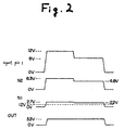
- the signal generator showing the first embodiment of the present invention is put in an enabled state when a potential 12V higher than a recommended input high voltage (for example 6.5V) is applied to a predetermined input pin 1.
- a recommended input high voltage for example 6.5V
- n-MOS transistors Q1 ⁇ Q6 (a high impedance circuit) are successively turned on. Thereafter, a potential level of a first node N1 is in an H level state.
- the signal amplifier 2 amplifies the potential of the first node N1 and the output terminal rises to 3.3V.
- the H level signal is outputted from the output terminal in response to an operation as described above. Thereafter, the H level signal is used as a test mode signal.
- the n-MOS transistors Q8 turns on in response to the H level of the output terminal.
- a current path between the first node N1 and the second node N2 is bypassed in response to which the n-MOS transistors Q8 turns on. Therefore, the current path between the first node N1 and the second node N2 is put in a conductive state.
- the lower voltage has a value sufficient to maintain the n-MOS transistors (Q1 ⁇ Q3) in an on state and to maintain a potential at the first node N1 higher than a threshold voltage of the signal amplifier 2.
- the lower voltage is 8V in the first embodiment of the present invention.
- the n-MOS transistors (Q1 ⁇ Q3) are in an off state.
- the signal amplifier 2 also enters an off state.
- the n-MOS transistor Q7 completely sets the first node N1 in an L level state. Therefore, the output of the test mode signal stops in response to an operation as described above and a test mode switches to a normal mode.
- the signal generator of the first embodiment shown in Fig. 1 needs to apply an input voltage (for example, 12V) higher than a recommended input high voltage to the input pin 1 until the n-MOS transistor Q8 enters an on state.
- an input voltage for example, 12V
- a recommended input high voltage for example, 8V
- the signal generator of the first embodiment doesn't need to continue applying an input voltage higher than a recommended input high voltage to the input pin 1.
- gate oxide breakdown of a transistor can be prevented from occurring when a test mode signal is outputted.
- the signal amplifier 2 is comprised of a plurality of invertors which are formed of the n-MOS transistor and the p-MOS transistor. Since a first stage invertor of an input side of the signal amplifier 2 has a threshold voltage lower than other invertors of the signal amplifier 2, the signal generator of the first embodiment is more sensitive to a change of a potential at the node N1.
- the p-MOS transistor constructing the first stage invertor has a lower driving ability than the n-MOS transistor. Specifically, a gate width of the p-MOS transistor is shorter than a gate width of the n-MOS transistor, or a gate length of the p-MOS transistor is longer than a gate length of the n-MOS transistor. Therefore, it is possible to secure low voltage applied to the input pin 1, and to prevent a leakage current from the input pin 1 to Vss.
- Fig. 3 is a circuit diagram of a signal generator showing a second embodiment of the present invention.
- the signal generator shown in Fig. 3 comprises: an input pin 1; a high impedance circuit being coupled with the input pin 1, the high impedance circuit comprising a plurality of n-MOS transistors (Q1 ⁇ Q6), the plurality of n-MOS transistors (Q1 ⁇ Q6) respectively being connected in series and respectively having a gate coupled with a source or a drain; a signal amplifier 2 comprising a plurality of invertor circuits being coupled with an n-MOS transistor Q6 toward an output side of the plurality of n-MOS transistors (Q1 ⁇ Q6), having an output terminal for outputting a test mode signal, and being coupled with the high impedance circuit through a first node N1; a resistor being coupled between an n-MOS transistor Q6 and reference voltage (for example Vss) through the first node N1; an n-MOS transistor Q7 constantly applying 1/2 Vcc to a gate of the n-MOS transistor Q7; an n-MOS transistor Q8 being coupled
- the n-MOS transistor Q8 bypasses a current path from the second node N2 to the first node N1 and maintains a potential level of the first node N1, in response to an output condition of the signal amplifier 2.
- the n-MOS transistor Q9 bypasses a current path from the third node N3 to the first node N1 and supplies a predetermined potential to the first node N1, in response to an input of a control signal INTBB, and a situation where any voltage higher than a recommended input high voltage is applied to a predetermined input pin 1.
- n-MOS transistor Q7 acting as a resistor constantly applies 1/2 Vcc to a gate of the n-MOS transistor Q7, a potential of the node between the input pin 1 and a drain of the n-MOS transistor Q1 correlates with a potential of the first node N1.
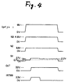
- the signal generator showing the second embodiment of the present invention is put in an enabled state when 12V higher than a recommended input high voltage( for example 6.5V) is applied to a predetermined input pin 1.
- n-MOS transistors Q1 and Q2 are successively turned on.
- a control signal INTBB for example 3.3V
- a current path between a third node N3 and a first node N1 is in a conductive state. Therefore, a potential level of a first node N1 is in an H level state.
- the signal amplifier 2 amplifies the potential of the first node N1 and the output terminal rises to 3.3V.
- the H level signal is outputted from the output terminal in response to an operation as described above, the H level signal is thereafter used as a test mode signal.
- the n-MOS transistors Q8 turns on in response to the H level of the output terminal.
- a current path between the first node N1 and the second node N2 is bypassed in response to which the n-MOS transistors Q8 turns on. Therefore, the current path between the first node N1 and the second node N2 will become conductive .
- the lower voltage has a value sufficient to maintain an on state of the n-MOS transistors (Q1 ⁇ Q3) and to maintain a potential higher than a threshold voltage of the signal amplifier 2 at the first node N1.
- the lower voltage is 8V in the second embodiment of the present invention.
- the potential of the first node N1 falls and the signal amplifier 2 is also in an off state.
- a potential of the output terminal also falls and the n-MOS transistor Q8 is in an off state.
- the n-MOS transistor Q7 completely sets the first node N1 to an L level state. Therefore, the output of the test mode signal stops in response to an operation as described above and a test mode switches to a normal mode.
- the control signal INTBB is maintained at an H level until the n-MOS transistor Q8 is in an on state.
- the lower voltage applied to the input pin 1 is preferably sufficient to put at least the n-MOS transistors Q1 and Q2 in an on state and to maintain a potential higher than a threshold value of the signal amplifier 2 at the first node N1, until the test mode signal is outputted from the output terminal OUT.
- the lower voltage is 8V.
- n-MOS transistor Q8 is put an on state
- a voltage sufficient to put the n-MOS transistors Q1, Q2, Q3 is in an on state is preferably applied to the input pin 1, for example, 8V.
- the second embodiment of the present invention does not need to apply an input voltage (for example, 12V) higher than a recommended input high voltage to the input pin 1.
- an input voltage for example, 12V
- the second embodiment of the present invention is able to provide a signal generator that switches from a normal mode to a test mode at a lower voltage than in the conventional art, gate oxidation layer breakdown of a transistor can be prevented from occurring when a test mode signal is outputted.
- the signal generator of the second embodiment is more sensitive to a change of a potential at the node N1. Therefore, the p-MOS transistor constructing the first stage invertor has a driving ability lower than the n-MOS transistor. Specifically, a gate width of the p-MOS transistor is shorter than a gate width of the n-MOS transistor, or a gate length of the p-MOS transistor is longer than a gate length of the n-MOS transistor. Therefore, it is possible to secure a low voltage applied to the input pin 1, and to prevent a leakage current from the input pin 1 to Vss.
- a signal generator of an another embodiment comprising: an input pin; a circuit being coupled between the input pin and a first node, the circuit comprising a plurality of transistors, the plurality of transistors respectively being connected in series and respectively having a gate coupled with a source or a drain; a signal amplifier being coupled with the circuit through the first node; a resistor being coupled between the first node and a reference voltage; a first transistor being coupled between the first node and a second node between a predetermined transistors among the plurality of transistors, the first transistor bypassing a current path from the second node to the first node and supplying a predetermined potential to the first node, in response to an input of a control signal and an output condition of the signal amplifier; and a second transistor being coupled between the first node and the second node, the second transistor bypassing a current path from the second node to the first node and maintaining the predetermined potential of the first node, in response to the output condition of the signal amplifier.
- n-MOS transistors (Q1 ⁇ Q6) shown in Fig. 1, 3 may have the source connected to the gate, respectively, for
Landscapes
- Engineering & Computer Science (AREA)
- General Engineering & Computer Science (AREA)
- Physics & Mathematics (AREA)
- General Physics & Mathematics (AREA)
- Microelectronics & Electronic Packaging (AREA)
- Computer Hardware Design (AREA)
- Amplifiers (AREA)
- Tests Of Electronic Circuits (AREA)
- Dram (AREA)
- Measurement Of Current Or Voltage (AREA)
- For Increasing The Reliability Of Semiconductor Memories (AREA)
- Logic Circuits (AREA)
Applications Claiming Priority (3)
| Application Number | Priority Date | Filing Date | Title |
|---|---|---|---|
| JP01423296A JP3609185B2 (ja) | 1996-01-30 | 1996-01-30 | 信号発生回路及びこれを用いたテストモード設定方法 |
| JP1423296 | 1996-01-30 | ||
| JP14232/96 | 1996-01-30 |
Publications (2)
| Publication Number | Publication Date |
|---|---|
| EP0788116A1 true EP0788116A1 (fr) | 1997-08-06 |
| EP0788116B1 EP0788116B1 (fr) | 2001-07-11 |
Family
ID=11855335
Family Applications (1)
| Application Number | Title | Priority Date | Filing Date |
|---|---|---|---|
| EP97101232A Expired - Lifetime EP0788116B1 (fr) | 1996-01-30 | 1997-01-27 | Circuit de détection de surtension pour sélection de mode |
Country Status (7)
| Country | Link |
|---|---|
| US (1) | US5786716A (fr) |
| EP (1) | EP0788116B1 (fr) |
| JP (1) | JP3609185B2 (fr) |
| KR (1) | KR100337674B1 (fr) |
| CN (1) | CN1158671C (fr) |
| DE (1) | DE69705553T2 (fr) |
| TW (1) | TW367411B (fr) |
Cited By (1)
| Publication number | Priority date | Publication date | Assignee | Title |
|---|---|---|---|---|
| FR2794867A1 (fr) * | 1999-06-08 | 2000-12-15 | St Microelectronics Sa | Circuit de detection et de memorisation d'une surtension |
Families Citing this family (8)
| Publication number | Priority date | Publication date | Assignee | Title |
|---|---|---|---|---|
| CN1092335C (zh) | 1995-08-21 | 2002-10-09 | 松下电器产业株式会社 | 电压检测电路、电源通-断复位电路及半导体装置 |
| JP3288249B2 (ja) * | 1997-03-31 | 2002-06-04 | 東芝マイクロエレクトロニクス株式会社 | パワーオンリセット回路 |
| DE19819265C1 (de) * | 1998-04-30 | 1999-08-19 | Micronas Intermetall Gmbh | Verfahren zum Parametrieren einer integrierten Schaltungsanordnung und integrierte Schaltungsanordnung hierfür |
| JP2003132674A (ja) | 2001-10-26 | 2003-05-09 | Mitsubishi Electric Corp | 半導体記憶装置 |
| BR0313529A (pt) * | 2002-08-16 | 2005-07-12 | Boc Group Inc | Método e aparelho para congelar crosta superficial de produto alimentìcio |
| CN100403034C (zh) * | 2003-12-30 | 2008-07-16 | 上海贝岭股份有限公司 | 低功耗低温漂与工艺无关的电压检测电路 |
| CN100356179C (zh) * | 2004-09-29 | 2007-12-19 | 华为技术有限公司 | 一种信号发生装置和方法 |
| USD587293S1 (en) * | 2008-05-23 | 2009-02-24 | Martinez M Dawn | Decorated eyewear |
Citations (3)
| Publication number | Priority date | Publication date | Assignee | Title |
|---|---|---|---|---|
| EP0238283A2 (fr) * | 1986-03-19 | 1987-09-23 | Fujitsu Limited | Circuit pour détecter des hautes tensions |
| EP0255362A2 (fr) * | 1986-08-01 | 1988-02-03 | Fujitsu Limited | Circuit intégré à semi-conducteur |
| EP0399207A2 (fr) * | 1989-05-23 | 1990-11-28 | International Business Machines Corporation | Système de contrôle de sélection |
Family Cites Families (1)
| Publication number | Priority date | Publication date | Assignee | Title |
|---|---|---|---|---|
| ATE137872T1 (de) * | 1991-02-21 | 1996-05-15 | Siemens Ag | Regelschaltung für einen substratvorspannungsgenerator |
-
1996
- 1996-01-30 JP JP01423296A patent/JP3609185B2/ja not_active Expired - Fee Related
-
1997
- 1997-01-23 US US08/788,121 patent/US5786716A/en not_active Expired - Lifetime
- 1997-01-25 TW TW086100846A patent/TW367411B/zh not_active IP Right Cessation
- 1997-01-27 EP EP97101232A patent/EP0788116B1/fr not_active Expired - Lifetime
- 1997-01-27 DE DE69705553T patent/DE69705553T2/de not_active Expired - Lifetime
- 1997-01-30 KR KR1019970002749A patent/KR100337674B1/ko not_active Expired - Fee Related
- 1997-01-30 CN CNB971031932A patent/CN1158671C/zh not_active Expired - Fee Related
Patent Citations (3)
| Publication number | Priority date | Publication date | Assignee | Title |
|---|---|---|---|---|
| EP0238283A2 (fr) * | 1986-03-19 | 1987-09-23 | Fujitsu Limited | Circuit pour détecter des hautes tensions |
| EP0255362A2 (fr) * | 1986-08-01 | 1988-02-03 | Fujitsu Limited | Circuit intégré à semi-conducteur |
| EP0399207A2 (fr) * | 1989-05-23 | 1990-11-28 | International Business Machines Corporation | Système de contrôle de sélection |
Cited By (2)
| Publication number | Priority date | Publication date | Assignee | Title |
|---|---|---|---|---|
| FR2794867A1 (fr) * | 1999-06-08 | 2000-12-15 | St Microelectronics Sa | Circuit de detection et de memorisation d'une surtension |
| US6411544B1 (en) | 1999-06-08 | 2002-06-25 | Stmicroelectronics S.A. | Circuit for detecting and recording a voltage surge |
Also Published As
| Publication number | Publication date |
|---|---|
| EP0788116B1 (fr) | 2001-07-11 |
| TW367411B (en) | 1999-08-21 |
| DE69705553D1 (de) | 2001-08-16 |
| CN1162820A (zh) | 1997-10-22 |
| KR100337674B1 (ko) | 2002-07-18 |
| JPH09204798A (ja) | 1997-08-05 |
| CN1158671C (zh) | 2004-07-21 |
| US5786716A (en) | 1998-07-28 |
| DE69705553T2 (de) | 2002-05-29 |
| KR970060248A (ko) | 1997-08-12 |
| JP3609185B2 (ja) | 2005-01-12 |
Similar Documents
| Publication | Publication Date | Title |
|---|---|---|
| US6038189A (en) | Semiconductor device allowing external setting of internal power supply voltage generated by a voltage down converter at the time of testing | |
| US5283762A (en) | Semiconductor device containing voltage converting circuit and operating method thereof | |
| US5828596A (en) | Semiconductor memory device | |
| KR930009025B1 (ko) | 반도체집적회로 장치 | |
| US6867641B2 (en) | Internal voltage generator for semiconductor device | |
| EP0788116B1 (fr) | Circuit de détection de surtension pour sélection de mode | |
| US6628162B2 (en) | Semiconductor integrated circuit | |
| US6064233A (en) | Semiconductor integrated circuit measuring current to test damaged transistor | |
| US9374092B2 (en) | Internal voltage compensation circuit | |
| US5942808A (en) | Semiconductor device with plural power supply circuits, plural internal circuits, and single external terminal | |
| KR100302424B1 (ko) | 논리하이브리드메모리용반도체메모리 | |
| US7279955B2 (en) | Reference voltage generating circuit | |
| US5966045A (en) | Semiconductor device having a first stage input unit to which a potential is supplied from external and internal power supplies | |
| US6333880B1 (en) | Semiconductor memory device capable of detecting high-voltage test command signal | |
| US6353560B1 (en) | Semiconductor memory device | |
| US6191987B1 (en) | Semiconductor memory test circuit | |
| KR19980028831A (ko) | 반도체 메모리장치 | |
| US5124587A (en) | Integrated circuit with a configuration circuit | |
| US20030011405A1 (en) | Semiconductor integrated circuit | |
| US20040037149A1 (en) | Semiconductor memory device capable of normal transition to test mode | |
| US6898745B2 (en) | Integrated device with operativity testing | |
| KR100239884B1 (ko) | 전압 레벨 쉬프트 회로 | |
| KR100231430B1 (ko) | 반도체 메모리소자의 데이터출력 버퍼회로 | |
| KR100253646B1 (ko) | 반도체메모리장치의시그너쳐회로. | |
| KR100481825B1 (ko) | 워드라인전압발생회로를갖는반도체메모리장치 |
Legal Events
| Date | Code | Title | Description |
|---|---|---|---|
| PUAI | Public reference made under article 153(3) epc to a published international application that has entered the european phase |
Free format text: ORIGINAL CODE: 0009012 |
|
| AK | Designated contracting states |
Kind code of ref document: A1 Designated state(s): DE FR NL |
|
| 17P | Request for examination filed |
Effective date: 19971010 |
|
| GRAG | Despatch of communication of intention to grant |
Free format text: ORIGINAL CODE: EPIDOS AGRA |
|
| 17Q | First examination report despatched |
Effective date: 20001004 |
|
| GRAG | Despatch of communication of intention to grant |
Free format text: ORIGINAL CODE: EPIDOS AGRA |
|
| GRAH | Despatch of communication of intention to grant a patent |
Free format text: ORIGINAL CODE: EPIDOS IGRA |
|
| GRAH | Despatch of communication of intention to grant a patent |
Free format text: ORIGINAL CODE: EPIDOS IGRA |
|
| GRAA | (expected) grant |
Free format text: ORIGINAL CODE: 0009210 |
|
| AK | Designated contracting states |
Kind code of ref document: B1 Designated state(s): DE FR NL |
|
| REF | Corresponds to: |
Ref document number: 69705553 Country of ref document: DE Date of ref document: 20010816 |
|
| ET | Fr: translation filed | ||
| PLBE | No opposition filed within time limit |
Free format text: ORIGINAL CODE: 0009261 |
|
| STAA | Information on the status of an ep patent application or granted ep patent |
Free format text: STATUS: NO OPPOSITION FILED WITHIN TIME LIMIT |
|
| 26N | No opposition filed | ||
| REG | Reference to a national code |
Ref country code: FR Ref legal event code: TP |
|
| PGFP | Annual fee paid to national office [announced via postgrant information from national office to epo] |
Ref country code: FR Payment date: 20110128 Year of fee payment: 15 Ref country code: NL Payment date: 20110120 Year of fee payment: 15 Ref country code: DE Payment date: 20110119 Year of fee payment: 15 |
|
| REG | Reference to a national code |
Ref country code: NL Ref legal event code: V1 Effective date: 20120801 |
|
| REG | Reference to a national code |
Ref country code: FR Ref legal event code: ST Effective date: 20120928 |
|
| PG25 | Lapsed in a contracting state [announced via postgrant information from national office to epo] |
Ref country code: DE Free format text: LAPSE BECAUSE OF NON-PAYMENT OF DUE FEES Effective date: 20120801 |
|
| REG | Reference to a national code |
Ref country code: DE Ref legal event code: R119 Ref document number: 69705553 Country of ref document: DE Effective date: 20120801 |
|
| PG25 | Lapsed in a contracting state [announced via postgrant information from national office to epo] |
Ref country code: FR Free format text: LAPSE BECAUSE OF NON-PAYMENT OF DUE FEES Effective date: 20120131 |
|
| PG25 | Lapsed in a contracting state [announced via postgrant information from national office to epo] |
Ref country code: NL Free format text: LAPSE BECAUSE OF NON-PAYMENT OF DUE FEES Effective date: 20120801 |