EP0788120A1 - Gegenstände mit weichmagnetischen Dünnschichten und ihr Herstellungsverfahren - Google Patents
Gegenstände mit weichmagnetischen Dünnschichten und ihr Herstellungsverfahren Download PDFInfo
- Publication number
- EP0788120A1 EP0788120A1 EP97300373A EP97300373A EP0788120A1 EP 0788120 A1 EP0788120 A1 EP 0788120A1 EP 97300373 A EP97300373 A EP 97300373A EP 97300373 A EP97300373 A EP 97300373A EP 0788120 A1 EP0788120 A1 EP 0788120A1
- Authority
- EP
- European Patent Office
- Prior art keywords
- approximately
- magnetically soft
- alloy
- thin film
- range
- Prior art date
- Legal status (The legal status is an assumption and is not a legal conclusion. Google has not performed a legal analysis and makes no representation as to the accuracy of the status listed.)
- Ceased
Links
- 239000010409 thin film Substances 0.000 title claims abstract description 43
- 238000000034 method Methods 0.000 title claims abstract description 25
- 239000010408 film Substances 0.000 claims abstract description 97
- 230000005291 magnetic effect Effects 0.000 claims abstract description 84
- 229910045601 alloy Inorganic materials 0.000 claims abstract description 41
- 239000000956 alloy Substances 0.000 claims abstract description 41
- 230000005415 magnetization Effects 0.000 claims abstract description 19
- 229910052715 tantalum Inorganic materials 0.000 claims abstract description 17
- 229910052735 hafnium Inorganic materials 0.000 claims abstract description 16
- 239000010955 niobium Substances 0.000 claims abstract description 16
- 239000010936 titanium Substances 0.000 claims abstract description 16
- 229910052750 molybdenum Inorganic materials 0.000 claims abstract description 13
- 229910052758 niobium Inorganic materials 0.000 claims abstract description 13
- 229910052719 titanium Inorganic materials 0.000 claims abstract description 13
- 229910052721 tungsten Inorganic materials 0.000 claims abstract description 13
- RGJYWVHOPDRGDB-UHFFFAOYSA-N [N].[Cr].[Fe] Chemical compound [N].[Cr].[Fe] RGJYWVHOPDRGDB-UHFFFAOYSA-N 0.000 claims abstract description 4
- ZOKXTWBITQBERF-UHFFFAOYSA-N Molybdenum Chemical compound [Mo] ZOKXTWBITQBERF-UHFFFAOYSA-N 0.000 claims abstract description 3
- RTAQQCXQSZGOHL-UHFFFAOYSA-N Titanium Chemical compound [Ti] RTAQQCXQSZGOHL-UHFFFAOYSA-N 0.000 claims abstract description 3
- VBJZVLUMGGDVMO-UHFFFAOYSA-N hafnium atom Chemical compound [Hf] VBJZVLUMGGDVMO-UHFFFAOYSA-N 0.000 claims abstract description 3
- 239000011733 molybdenum Substances 0.000 claims abstract description 3
- GUCVJGMIXFAOAE-UHFFFAOYSA-N niobium atom Chemical compound [Nb] GUCVJGMIXFAOAE-UHFFFAOYSA-N 0.000 claims abstract description 3
- VSZWPYCFIRKVQL-UHFFFAOYSA-N selanylidenegallium;selenium Chemical compound [Se].[Se]=[Ga].[Se]=[Ga] VSZWPYCFIRKVQL-UHFFFAOYSA-N 0.000 claims abstract description 3
- WFKWXMTUELFFGS-UHFFFAOYSA-N tungsten Chemical compound [W] WFKWXMTUELFFGS-UHFFFAOYSA-N 0.000 claims abstract description 3
- 239000010937 tungsten Substances 0.000 claims abstract description 3
- LEONUFNNVUYDNQ-UHFFFAOYSA-N vanadium atom Chemical compound [V] LEONUFNNVUYDNQ-UHFFFAOYSA-N 0.000 claims abstract description 3
- IJGRMHOSHXDMSA-UHFFFAOYSA-N Atomic nitrogen Chemical compound N#N IJGRMHOSHXDMSA-UHFFFAOYSA-N 0.000 claims description 42
- 239000000758 substrate Substances 0.000 claims description 38
- 229910052757 nitrogen Inorganic materials 0.000 claims description 37
- 238000000151 deposition Methods 0.000 claims description 24
- 238000004544 sputter deposition Methods 0.000 claims description 24
- 239000000203 mixture Substances 0.000 claims description 22
- 229910052804 chromium Inorganic materials 0.000 claims description 15
- 229910052742 iron Inorganic materials 0.000 claims description 11
- 229910052720 vanadium Inorganic materials 0.000 claims description 10
- 229910052726 zirconium Inorganic materials 0.000 claims description 10
- 125000006850 spacer group Chemical group 0.000 claims description 4
- 230000005290 antiferromagnetic effect Effects 0.000 claims description 3
- 230000005294 ferromagnetic effect Effects 0.000 claims description 3
- 238000001704 evaporation Methods 0.000 claims description 2
- 230000008020 evaporation Effects 0.000 claims description 2
- 238000007737 ion beam deposition Methods 0.000 claims description 2
- 238000005468 ion implantation Methods 0.000 claims description 2
- 238000000608 laser ablation Methods 0.000 claims description 2
- 229910019590 Cr-N Inorganic materials 0.000 claims 2
- 229910019588 Cr—N Inorganic materials 0.000 claims 2
- KKPVDVIXVRHTQQ-UHFFFAOYSA-N [N].[Ta].[Cr].[Fe] Chemical compound [N].[Ta].[Cr].[Fe] KKPVDVIXVRHTQQ-UHFFFAOYSA-N 0.000 claims 1
- 239000002885 antiferromagnetic material Substances 0.000 claims 1
- 239000002902 ferrimagnetic material Substances 0.000 claims 1
- 239000003302 ferromagnetic material Substances 0.000 claims 1
- GUVRBAGPIYLISA-UHFFFAOYSA-N tantalum atom Chemical compound [Ta] GUVRBAGPIYLISA-UHFFFAOYSA-N 0.000 abstract description 2
- 239000010410 layer Substances 0.000 description 22
- XEEYBQQBJWHFJM-UHFFFAOYSA-N iron Substances [Fe] XEEYBQQBJWHFJM-UHFFFAOYSA-N 0.000 description 16
- 230000008021 deposition Effects 0.000 description 15
- 229920001721 polyimide Polymers 0.000 description 11
- 239000004642 Polyimide Substances 0.000 description 10
- 238000010586 diagram Methods 0.000 description 10
- 239000007789 gas Substances 0.000 description 10
- 239000000463 material Substances 0.000 description 10
- 238000010438 heat treatment Methods 0.000 description 9
- XKRFYHLGVUSROY-UHFFFAOYSA-N Argon Chemical compound [Ar] XKRFYHLGVUSROY-UHFFFAOYSA-N 0.000 description 8
- 230000008569 process Effects 0.000 description 8
- 229910001199 N alloy Inorganic materials 0.000 description 7
- PXHVJJICTQNCMI-UHFFFAOYSA-N nickel Substances [Ni] PXHVJJICTQNCMI-UHFFFAOYSA-N 0.000 description 7
- 238000005546 reactive sputtering Methods 0.000 description 6
- 239000004020 conductor Substances 0.000 description 5
- 230000007797 corrosion Effects 0.000 description 5
- 238000005260 corrosion Methods 0.000 description 5
- 229910052751 metal Inorganic materials 0.000 description 5
- QJGQUHMNIGDVPM-UHFFFAOYSA-N nitrogen group Chemical group [N] QJGQUHMNIGDVPM-UHFFFAOYSA-N 0.000 description 5
- 230000003647 oxidation Effects 0.000 description 5
- 238000007254 oxidation reaction Methods 0.000 description 5
- -1 Cr-nitride Chemical class 0.000 description 4
- 229910017060 Fe Cr Inorganic materials 0.000 description 4
- 229910002544 Fe-Cr Inorganic materials 0.000 description 4
- XUIMIQQOPSSXEZ-UHFFFAOYSA-N Silicon Chemical compound [Si] XUIMIQQOPSSXEZ-UHFFFAOYSA-N 0.000 description 4
- 229910052786 argon Inorganic materials 0.000 description 4
- UPHIPHFJVNKLMR-UHFFFAOYSA-N chromium iron Chemical compound [Cr].[Fe] UPHIPHFJVNKLMR-UHFFFAOYSA-N 0.000 description 4
- 230000035699 permeability Effects 0.000 description 4
- 229920000642 polymer Polymers 0.000 description 4
- 229910052710 silicon Inorganic materials 0.000 description 4
- 239000010703 silicon Substances 0.000 description 4
- 229910052782 aluminium Inorganic materials 0.000 description 3
- 239000002131 composite material Substances 0.000 description 3
- 239000010949 copper Substances 0.000 description 3
- 238000013461 design Methods 0.000 description 3
- 229910001873 dinitrogen Inorganic materials 0.000 description 3
- 238000003475 lamination Methods 0.000 description 3
- 238000001755 magnetron sputter deposition Methods 0.000 description 3
- 239000011572 manganese Substances 0.000 description 3
- 229910052759 nickel Inorganic materials 0.000 description 3
- 150000004767 nitrides Chemical class 0.000 description 3
- 238000012545 processing Methods 0.000 description 3
- 238000005477 sputtering target Methods 0.000 description 3
- JBRZTFJDHDCESZ-UHFFFAOYSA-N AsGa Chemical compound [As]#[Ga] JBRZTFJDHDCESZ-UHFFFAOYSA-N 0.000 description 2
- OKTJSMMVPCPJKN-UHFFFAOYSA-N Carbon Chemical compound [C] OKTJSMMVPCPJKN-UHFFFAOYSA-N 0.000 description 2
- 229910052684 Cerium Inorganic materials 0.000 description 2
- 229910001218 Gallium arsenide Inorganic materials 0.000 description 2
- PWHULOQIROXLJO-UHFFFAOYSA-N Manganese Chemical compound [Mn] PWHULOQIROXLJO-UHFFFAOYSA-N 0.000 description 2
- 238000005275 alloying Methods 0.000 description 2
- XAGFODPZIPBFFR-UHFFFAOYSA-N aluminium Chemical compound [Al] XAGFODPZIPBFFR-UHFFFAOYSA-N 0.000 description 2
- 125000004429 atom Chemical group 0.000 description 2
- 230000015572 biosynthetic process Effects 0.000 description 2
- 229910052799 carbon Inorganic materials 0.000 description 2
- GWXLDORMOJMVQZ-UHFFFAOYSA-N cerium Chemical compound [Ce] GWXLDORMOJMVQZ-UHFFFAOYSA-N 0.000 description 2
- 230000008859 change Effects 0.000 description 2
- 239000010941 cobalt Substances 0.000 description 2
- 229910017052 cobalt Inorganic materials 0.000 description 2
- GUTLYIVDDKVIGB-UHFFFAOYSA-N cobalt atom Chemical compound [Co] GUTLYIVDDKVIGB-UHFFFAOYSA-N 0.000 description 2
- KPLQYGBQNPPQGA-UHFFFAOYSA-N cobalt samarium Chemical compound [Co].[Sm] KPLQYGBQNPPQGA-UHFFFAOYSA-N 0.000 description 2
- 238000004090 dissolution Methods 0.000 description 2
- 230000006870 function Effects 0.000 description 2
- 239000012535 impurity Substances 0.000 description 2
- 238000009413 insulation Methods 0.000 description 2
- 229910052746 lanthanum Inorganic materials 0.000 description 2
- FZLIPJUXYLNCLC-UHFFFAOYSA-N lanthanum atom Chemical compound [La] FZLIPJUXYLNCLC-UHFFFAOYSA-N 0.000 description 2
- 229910052748 manganese Inorganic materials 0.000 description 2
- 238000004519 manufacturing process Methods 0.000 description 2
- 230000015654 memory Effects 0.000 description 2
- 239000002184 metal Substances 0.000 description 2
- 150000002739 metals Chemical class 0.000 description 2
- 229910001172 neodymium magnet Inorganic materials 0.000 description 2
- 125000004433 nitrogen atom Chemical group N* 0.000 description 2
- 229910000889 permalloy Inorganic materials 0.000 description 2
- 229910052761 rare earth metal Inorganic materials 0.000 description 2
- 150000002910 rare earth metals Chemical class 0.000 description 2
- 229910000938 samarium–cobalt magnet Inorganic materials 0.000 description 2
- 239000004065 semiconductor Substances 0.000 description 2
- 238000001228 spectrum Methods 0.000 description 2
- 239000000126 substance Substances 0.000 description 2
- 238000000427 thin-film deposition Methods 0.000 description 2
- 229910052723 transition metal Inorganic materials 0.000 description 2
- 150000003624 transition metals Chemical class 0.000 description 2
- 238000004804 winding Methods 0.000 description 2
- RYGMFSIKBFXOCR-UHFFFAOYSA-N Copper Chemical compound [Cu] RYGMFSIKBFXOCR-UHFFFAOYSA-N 0.000 description 1
- 229910017110 Fe—Cr—Co Inorganic materials 0.000 description 1
- 229910003271 Ni-Fe Inorganic materials 0.000 description 1
- GRYLNZFGIOXLOG-UHFFFAOYSA-N Nitric acid Chemical compound O[N+]([O-])=O GRYLNZFGIOXLOG-UHFFFAOYSA-N 0.000 description 1
- QJVKUMXDEUEQLH-UHFFFAOYSA-N [B].[Fe].[Nd] Chemical compound [B].[Fe].[Nd] QJVKUMXDEUEQLH-UHFFFAOYSA-N 0.000 description 1
- WBWJXRJARNTNBL-UHFFFAOYSA-N [Fe].[Cr].[Co] Chemical compound [Fe].[Cr].[Co] WBWJXRJARNTNBL-UHFFFAOYSA-N 0.000 description 1
- LAKFTXSXDDJHPQ-UHFFFAOYSA-N [Fe].[Hf] Chemical compound [Fe].[Hf] LAKFTXSXDDJHPQ-UHFFFAOYSA-N 0.000 description 1
- WGMRFRFZGVTCGH-UHFFFAOYSA-N [N].[Ta].[Fe] Chemical compound [N].[Ta].[Fe] WGMRFRFZGVTCGH-UHFFFAOYSA-N 0.000 description 1
- 238000004458 analytical method Methods 0.000 description 1
- 238000003491 array Methods 0.000 description 1
- 239000012159 carrier gas Substances 0.000 description 1
- 239000000919 ceramic Substances 0.000 description 1
- 238000005234 chemical deposition Methods 0.000 description 1
- 238000006243 chemical reaction Methods 0.000 description 1
- 238000000576 coating method Methods 0.000 description 1
- 230000001427 coherent effect Effects 0.000 description 1
- 230000000052 comparative effect Effects 0.000 description 1
- 150000001875 compounds Chemical class 0.000 description 1
- 229910052802 copper Inorganic materials 0.000 description 1
- 239000013078 crystal Substances 0.000 description 1
- 238000002425 crystallisation Methods 0.000 description 1
- 230000008025 crystallization Effects 0.000 description 1
- 238000005520 cutting process Methods 0.000 description 1
- 238000000354 decomposition reaction Methods 0.000 description 1
- 238000009792 diffusion process Methods 0.000 description 1
- 238000002845 discoloration Methods 0.000 description 1
- 230000005293 ferrimagnetic effect Effects 0.000 description 1
- 230000005350 ferromagnetic resonance Effects 0.000 description 1
- 230000004907 flux Effects 0.000 description 1
- 239000011521 glass Substances 0.000 description 1
- 238000002513 implantation Methods 0.000 description 1
- 238000010348 incorporation Methods 0.000 description 1
- 230000001939 inductive effect Effects 0.000 description 1
- UGKDIUIOSMUOAW-UHFFFAOYSA-N iron nickel Chemical compound [Fe].[Ni] UGKDIUIOSMUOAW-UHFFFAOYSA-N 0.000 description 1
- RNRAZTYOQURAEF-UHFFFAOYSA-N iron tantalum Chemical compound [Fe].[Fe].[Fe].[Fe].[Fe].[Fe].[Fe].[Ta].[Ta].[Ta] RNRAZTYOQURAEF-UHFFFAOYSA-N 0.000 description 1
- HZGFMPXURINDAW-UHFFFAOYSA-N iron zirconium Chemical compound [Fe].[Zr].[Zr] HZGFMPXURINDAW-UHFFFAOYSA-N 0.000 description 1
- 230000005381 magnetic domain Effects 0.000 description 1
- 239000000696 magnetic material Substances 0.000 description 1
- 230000005389 magnetism Effects 0.000 description 1
- 239000011159 matrix material Substances 0.000 description 1
- 238000012986 modification Methods 0.000 description 1
- 230000004048 modification Effects 0.000 description 1
- 229910017604 nitric acid Inorganic materials 0.000 description 1
- TWNQGVIAIRXVLR-UHFFFAOYSA-N oxo(oxoalumanyloxy)alumane Chemical compound O=[Al]O[Al]=O TWNQGVIAIRXVLR-UHFFFAOYSA-N 0.000 description 1
- AJCDFVKYMIUXCR-UHFFFAOYSA-N oxobarium;oxo(oxoferriooxy)iron Chemical compound [Ba]=O.O=[Fe]O[Fe]=O.O=[Fe]O[Fe]=O.O=[Fe]O[Fe]=O.O=[Fe]O[Fe]=O.O=[Fe]O[Fe]=O.O=[Fe]O[Fe]=O AJCDFVKYMIUXCR-UHFFFAOYSA-N 0.000 description 1
- 238000005289 physical deposition Methods 0.000 description 1
- 239000010453 quartz Substances 0.000 description 1
- 230000009467 reduction Effects 0.000 description 1
- 229920006395 saturated elastomer Polymers 0.000 description 1
- VYPSYNLAJGMNEJ-UHFFFAOYSA-N silicon dioxide Inorganic materials O=[Si]=O VYPSYNLAJGMNEJ-UHFFFAOYSA-N 0.000 description 1
- 239000002356 single layer Substances 0.000 description 1
- 239000007921 spray Substances 0.000 description 1
- 238000006467 substitution reaction Methods 0.000 description 1
- 238000010301 surface-oxidation reaction Methods 0.000 description 1
- 239000008399 tap water Substances 0.000 description 1
- 235000020679 tap water Nutrition 0.000 description 1
- 229910000859 α-Fe Inorganic materials 0.000 description 1
Images



Classifications
-
- G—PHYSICS
- G11—INFORMATION STORAGE
- G11B—INFORMATION STORAGE BASED ON RELATIVE MOVEMENT BETWEEN RECORD CARRIER AND TRANSDUCER
- G11B5/00—Recording by magnetisation or demagnetisation of a record carrier; Reproducing by magnetic means; Record carriers therefor
- G11B5/127—Structure or manufacture of heads, e.g. inductive
- G11B5/187—Structure or manufacture of the surface of the head in physical contact with, or immediately adjacent to the recording medium; Pole pieces; Gap features
- G11B5/1875—"Composite" pole pieces, i.e. poles composed in some parts of magnetic particles and in some other parts of magnetic metal layers
- G11B5/1877—"Composite" pole pieces, i.e. poles composed in some parts of magnetic particles and in some other parts of magnetic metal layers including at least one magnetic thin film
- G11B5/1878—"Composite" pole pieces, i.e. poles composed in some parts of magnetic particles and in some other parts of magnetic metal layers including at least one magnetic thin film disposed immediately adjacent to the transducing gap, e.g. "Metal-In-Gap" structure
-
- B—PERFORMING OPERATIONS; TRANSPORTING
- B82—NANOTECHNOLOGY
- B82Y—SPECIFIC USES OR APPLICATIONS OF NANOSTRUCTURES; MEASUREMENT OR ANALYSIS OF NANOSTRUCTURES; MANUFACTURE OR TREATMENT OF NANOSTRUCTURES
- B82Y25/00—Nanomagnetism, e.g. magnetoimpedance, anisotropic magnetoresistance, giant magnetoresistance or tunneling magnetoresistance
-
- B—PERFORMING OPERATIONS; TRANSPORTING
- B82—NANOTECHNOLOGY
- B82Y—SPECIFIC USES OR APPLICATIONS OF NANOSTRUCTURES; MEASUREMENT OR ANALYSIS OF NANOSTRUCTURES; MANUFACTURE OR TREATMENT OF NANOSTRUCTURES
- B82Y40/00—Manufacture or treatment of nanostructures
-
- G—PHYSICS
- G11—INFORMATION STORAGE
- G11B—INFORMATION STORAGE BASED ON RELATIVE MOVEMENT BETWEEN RECORD CARRIER AND TRANSDUCER
- G11B5/00—Recording by magnetisation or demagnetisation of a record carrier; Reproducing by magnetic means; Record carriers therefor
- G11B5/127—Structure or manufacture of heads, e.g. inductive
- G11B5/31—Structure or manufacture of heads, e.g. inductive using thin films
- G11B5/3109—Details
-
- G—PHYSICS
- G11—INFORMATION STORAGE
- G11B—INFORMATION STORAGE BASED ON RELATIVE MOVEMENT BETWEEN RECORD CARRIER AND TRANSDUCER
- G11B5/00—Recording by magnetisation or demagnetisation of a record carrier; Reproducing by magnetic means; Record carriers therefor
- G11B5/127—Structure or manufacture of heads, e.g. inductive
- G11B5/33—Structure or manufacture of flux-sensitive heads, i.e. for reproduction only; Combination of such heads with means for recording or erasing only
- G11B5/39—Structure or manufacture of flux-sensitive heads, i.e. for reproduction only; Combination of such heads with means for recording or erasing only using magneto-resistive devices or effects
- G11B5/3903—Structure or manufacture of flux-sensitive heads, i.e. for reproduction only; Combination of such heads with means for recording or erasing only using magneto-resistive devices or effects using magnetic thin film layers or their effects, the films being part of integrated structures
-
- G—PHYSICS
- G11—INFORMATION STORAGE
- G11B—INFORMATION STORAGE BASED ON RELATIVE MOVEMENT BETWEEN RECORD CARRIER AND TRANSDUCER
- G11B5/00—Recording by magnetisation or demagnetisation of a record carrier; Reproducing by magnetic means; Record carriers therefor
- G11B5/127—Structure or manufacture of heads, e.g. inductive
- G11B5/33—Structure or manufacture of flux-sensitive heads, i.e. for reproduction only; Combination of such heads with means for recording or erasing only
- G11B5/39—Structure or manufacture of flux-sensitive heads, i.e. for reproduction only; Combination of such heads with means for recording or erasing only using magneto-resistive devices or effects
- G11B5/3903—Structure or manufacture of flux-sensitive heads, i.e. for reproduction only; Combination of such heads with means for recording or erasing only using magneto-resistive devices or effects using magnetic thin film layers or their effects, the films being part of integrated structures
- G11B5/3906—Details related to the use of magnetic thin film layers or to their effects
-
- H—ELECTRICITY
- H01—ELECTRIC ELEMENTS
- H01F—MAGNETS; INDUCTANCES; TRANSFORMERS; SELECTION OF MATERIALS FOR THEIR MAGNETIC PROPERTIES
- H01F10/00—Thin magnetic films, e.g. of one-domain structure
- H01F10/002—Antiferromagnetic thin films, i.e. films exhibiting a Néel transition temperature
-
- H—ELECTRICITY
- H01—ELECTRIC ELEMENTS
- H01F—MAGNETS; INDUCTANCES; TRANSFORMERS; SELECTION OF MATERIALS FOR THEIR MAGNETIC PROPERTIES
- H01F10/00—Thin magnetic films, e.g. of one-domain structure
- H01F10/08—Thin magnetic films, e.g. of one-domain structure characterised by magnetic layers
-
- H—ELECTRICITY
- H01—ELECTRIC ELEMENTS
- H01F—MAGNETS; INDUCTANCES; TRANSFORMERS; SELECTION OF MATERIALS FOR THEIR MAGNETIC PROPERTIES
- H01F10/00—Thin magnetic films, e.g. of one-domain structure
- H01F10/08—Thin magnetic films, e.g. of one-domain structure characterised by magnetic layers
- H01F10/10—Thin magnetic films, e.g. of one-domain structure characterised by magnetic layers characterised by the composition
- H01F10/12—Thin magnetic films, e.g. of one-domain structure characterised by magnetic layers characterised by the composition being metals or alloys
- H01F10/13—Amorphous metallic alloys, e.g. glassy metals
-
- H—ELECTRICITY
- H01—ELECTRIC ELEMENTS
- H01F—MAGNETS; INDUCTANCES; TRANSFORMERS; SELECTION OF MATERIALS FOR THEIR MAGNETIC PROPERTIES
- H01F10/00—Thin magnetic films, e.g. of one-domain structure
- H01F10/08—Thin magnetic films, e.g. of one-domain structure characterised by magnetic layers
- H01F10/10—Thin magnetic films, e.g. of one-domain structure characterised by magnetic layers characterised by the composition
- H01F10/12—Thin magnetic films, e.g. of one-domain structure characterised by magnetic layers characterised by the composition being metals or alloys
- H01F10/13—Amorphous metallic alloys, e.g. glassy metals
- H01F10/138—Amorphous metallic alloys, e.g. glassy metals containing nanocrystallites, e.g. obtained by annealing
-
- H—ELECTRICITY
- H01—ELECTRIC ELEMENTS
- H01F—MAGNETS; INDUCTANCES; TRANSFORMERS; SELECTION OF MATERIALS FOR THEIR MAGNETIC PROPERTIES
- H01F10/00—Thin magnetic films, e.g. of one-domain structure
- H01F10/08—Thin magnetic films, e.g. of one-domain structure characterised by magnetic layers
- H01F10/10—Thin magnetic films, e.g. of one-domain structure characterised by magnetic layers characterised by the composition
- H01F10/12—Thin magnetic films, e.g. of one-domain structure characterised by magnetic layers characterised by the composition being metals or alloys
- H01F10/14—Thin magnetic films, e.g. of one-domain structure characterised by magnetic layers characterised by the composition being metals or alloys containing iron or nickel
- H01F10/147—Thin magnetic films, e.g. of one-domain structure characterised by magnetic layers characterised by the composition being metals or alloys containing iron or nickel with lattice under strain, e.g. expanded by interstitial nitrogen
-
- H—ELECTRICITY
- H01—ELECTRIC ELEMENTS
- H01F—MAGNETS; INDUCTANCES; TRANSFORMERS; SELECTION OF MATERIALS FOR THEIR MAGNETIC PROPERTIES
- H01F10/00—Thin magnetic films, e.g. of one-domain structure
- H01F10/32—Spin-exchange-coupled multilayers, e.g. nanostructured superlattices
- H01F10/3204—Exchange coupling of amorphous multilayers
-
- H—ELECTRICITY
- H01—ELECTRIC ELEMENTS
- H01F—MAGNETS; INDUCTANCES; TRANSFORMERS; SELECTION OF MATERIALS FOR THEIR MAGNETIC PROPERTIES
- H01F10/00—Thin magnetic films, e.g. of one-domain structure
- H01F10/32—Spin-exchange-coupled multilayers, e.g. nanostructured superlattices
- H01F10/324—Exchange coupling of magnetic film pairs via a very thin non-magnetic spacer, e.g. by exchange with conduction electrons of the spacer
- H01F10/3254—Exchange coupling of magnetic film pairs via a very thin non-magnetic spacer, e.g. by exchange with conduction electrons of the spacer the spacer being semiconducting or insulating, e.g. for spin tunnel junction [STJ]
-
- H—ELECTRICITY
- H01—ELECTRIC ELEMENTS
- H01F—MAGNETS; INDUCTANCES; TRANSFORMERS; SELECTION OF MATERIALS FOR THEIR MAGNETIC PROPERTIES
- H01F17/00—Fixed inductances of the signal type
- H01F17/0006—Printed inductances
- H01F17/0033—Printed inductances with the coil helically wound around a magnetic core
-
- H—ELECTRICITY
- H01—ELECTRIC ELEMENTS
- H01F—MAGNETS; INDUCTANCES; TRANSFORMERS; SELECTION OF MATERIALS FOR THEIR MAGNETIC PROPERTIES
- H01F41/00—Apparatus or processes specially adapted for manufacturing or assembling magnets, inductances or transformers; Apparatus or processes specially adapted for manufacturing materials characterised by their magnetic properties
- H01F41/14—Apparatus or processes specially adapted for manufacturing or assembling magnets, inductances or transformers; Apparatus or processes specially adapted for manufacturing materials characterised by their magnetic properties for applying magnetic films to substrates
- H01F41/30—Apparatus or processes specially adapted for manufacturing or assembling magnets, inductances or transformers; Apparatus or processes specially adapted for manufacturing materials characterised by their magnetic properties for applying magnetic films to substrates for applying nanostructures, e.g. by molecular beam epitaxy [MBE]
- H01F41/302—Apparatus or processes specially adapted for manufacturing or assembling magnets, inductances or transformers; Apparatus or processes specially adapted for manufacturing materials characterised by their magnetic properties for applying magnetic films to substrates for applying nanostructures, e.g. by molecular beam epitaxy [MBE] for applying spin-exchange-coupled multilayers, e.g. nanostructured superlattices
-
- Y—GENERAL TAGGING OF NEW TECHNOLOGICAL DEVELOPMENTS; GENERAL TAGGING OF CROSS-SECTIONAL TECHNOLOGIES SPANNING OVER SEVERAL SECTIONS OF THE IPC; TECHNICAL SUBJECTS COVERED BY FORMER USPC CROSS-REFERENCE ART COLLECTIONS [XRACs] AND DIGESTS
- Y10—TECHNICAL SUBJECTS COVERED BY FORMER USPC
- Y10S—TECHNICAL SUBJECTS COVERED BY FORMER USPC CROSS-REFERENCE ART COLLECTIONS [XRACs] AND DIGESTS
- Y10S428/00—Stock material or miscellaneous articles
- Y10S428/90—Magnetic feature
-
- Y—GENERAL TAGGING OF NEW TECHNOLOGICAL DEVELOPMENTS; GENERAL TAGGING OF CROSS-SECTIONAL TECHNOLOGIES SPANNING OVER SEVERAL SECTIONS OF THE IPC; TECHNICAL SUBJECTS COVERED BY FORMER USPC CROSS-REFERENCE ART COLLECTIONS [XRACs] AND DIGESTS
- Y10—TECHNICAL SUBJECTS COVERED BY FORMER USPC
- Y10T—TECHNICAL SUBJECTS COVERED BY FORMER US CLASSIFICATION
- Y10T428/00—Stock material or miscellaneous articles
- Y10T428/11—Magnetic recording head
- Y10T428/115—Magnetic layer composition
Definitions
- the invention relates to thin films of magnetically soft alloys. More particularly, the invention relates to articles comprising these alloys and methods for making such articles.
- Soft magnetic thin films are useful in modem, high-frequency, electromagnetic devices as a field-amplifying component, e.g., in the read-write head for magnetic disk memories in computers or as a core in microtransformers and inductors.
- desired properties of these films are relatively high saturation magnetization (4 ⁇ M s ), low coercivity (H c ), high permeability, high electrical resistivity and corrosion resistance.
- Various applications of soft magnetic thin films are described, for example, in books Magnetic Thin Films by R. F. Soohoo, Harper and Row, 1965; Thin Ferromagnetic Films by M. Prutton, Butterworth, 1964; and in articles C. R. Sullivan and S. R. Sanders, IEEE Trans. on Power Electronics, Proc. 24th Annual Power Electronics Specialists Conf., p. 33-40, June 1993; and T. Yachi et al., IEEE Trans. Magn. 28, 1969-1973 (1992).
- Ni-Fe nickel-iron
- Fe-based films such as 80% Ni-20% Fe (permalloy) are used most widely because of excellent magnetic properties and zero magnetostriction characteristics.
- Fe-based films such as iron-tantalum (Fe-Ta), iron-zirconium (Fe-Zr) and iron-hafnium (Fe-Hf) alloys generally exhibit higher saturation magnetization of 15-20 kilogauss (kG) as compared to about 10 kG for the 80% Ni permalloy films (see, e.g., N. Kataoka et al., Japanese J. Appl. Phys. 28, L462-L464, 1989, Trans. Jap. Inst. Metals 31, 429, 1990), however, they exhibit poorer soft magnetic properties and require post-deposition heat treatment.
- Fe-Ta-N iron-tantalum-nitrogen
- the required soft magnetic properties in the films it is desirable for the required soft magnetic properties in the films to be obtained in the as-deposited condition, or at the worst, with a very low temperature heat treatment below approximately 150°C where damage to polymers such as polyimide is kept relatively low.
- This application discloses new soft magnetic films with such desirable characteristics. Also, it is desirable to improve the corrosion/oxidation resistance of the Fe-rich thin films, as the oxides of iron and iron-rich alloys generally exhibit substantially reduced magnetic saturation. This application discloses thin films with improved corrosion resistance.
- the invention is embodied in a soft magnetic thin film article and methods for making such article.
- it is a soft magnetic thin film article comprising an iron-chromium-nitrogen (Fe-Cr-N) based alloy with tantalum in one embodiment and formed with at least one of the elements titanium (Ti), zirconium (Zr), hafnium (Hf), vanadium (V), molybdenum (Mo), niobium (Nb) or tungsten (W) in another embodiment.
- Fe-Cr-N iron-chromium-nitrogen
- the article is formed such that the alloy has a relatively high saturation magnetization (e.g., greater than approximately 15 kG) and a relatively low coercivity (e.g., less than approximately 2.0 oersteds) in an as-deposited condition or, alternatively, with a very low temperature treatment (e.g., below approximately 150°C).
- the inventive films are suitable for use in electromagnetic devices, for example, in microtransformer cores, inductor cores and in magnetic read-write heads.
- FIG. 1 is a block diagram showing one of the methods for making the Fe-Cr-N based soft magnetic thin films in accordance with the invention (i.e., soft magnetic thin films comprising Fe, Cr, N and either Ta or at least one of the following elements: Ti, Zr, Hf, V, Mo, Nb or W).
- a first step 110 is to provide an alloy target or targets from which the magnetic thin films of the invention are to be deposited, e.g., via chemical deposition or via physical deposition such as sputtering, evaporation, molecular beam epitaxial growth, ion beam deposition and laser ablation.
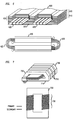
- the sputtering target (shown as 210 in FIG. 2a), which typically is in the form of a round plate, has, in one embodiment, the alloy composition similar to the desired film composition and has, in another embodiment, composite sections of different metals or alloys on the target surface to be sputtered away.
- the film deposition is accomplished by using multiple targets, e.g., by co-sputtering from two or more targets with different composition chosen so that the final composition of the deposited film on the substrate corresponds to the desired composition.
- two targets e.g., a Fe-5.3% Cr target on one side and a Ta or Hf target on the other side separated by approximately 6 inches
- triode sputtering generally is preferred because it uses lower bias voltage and lower Ar pressure, thus allowing easier control of the sputter deposition and the formation of desired nanocrystalline microstructure in the inventive Fe-Cr-N based soft magnetic films.
- nitrogen is incorporated into the alloy film by reactive deposition, i.e., by continuously supplying a specific partial pressure of nitrogen gas in the background Ar gas carrier during the sputtering process.
- the nitrogen atoms go into the thin film structure both by reaction with one or more of the metallic elements in the form of nitride, such as Cr-nitride, Fe-nitride, and/or Ta-nitride or a nitride of the remaining element Ti, Zr, Hf, V, Mo, Nb or W, and by dissolution in the form of interstitial solute atoms in the alloy crystal lattice.
- nitrogen is supplied by alloying it directly into the sputtering targets.
- nitrogen is added to the films after deposition, e.g., by ion implantation.
- thin films of inventive alloys, prepared by any suitable technique are subjected to nitrogen implantation with appropriate doses and processing temperatures.
- the desired composition of the target for the inventive film deposition is: Fe balance, Cr in the range of approximately 0.5-20.0 atomic %, preferably 1.0-12.0% and even more preferably 2.0-8.0 atomic %, and the remaining element in the range of approximately 0.1-10.0 atomic %, preferably 0.1-5.0%, and even more preferably 0.1-3.0%.
- the remaining element comprises Ta; in another embodiment, the remaining element comprises one or more elements chosen from Ti, Zr, Hf, V, Mo, Nb and W.
- the nitrogen atoms are incorporated in the target, the desired composition is 1.0-30.0 atomic %, preferably 2.0-20.0%, even more preferably 2.0-15.0%. If nitrogen is to be added by reactive sputtering, the alloy target has 0.0-20.0% nitrogen depending on the concentration of the nitrogen gas used during the sputtering.
- the next step 120 is to provide a substrate onto which the inventive magnetic film is to be deposited.
- a clean and smooth non-magnetic substrate surface is desired for microtransformer-type applications.
- Desirable substrate materials include, e.g., semiconductors such as silicon (Si) and gallium-arsenide (Ga-As), and other materials such as glass, quartz, ceramics, polymers and polyimide.
- Si silicon
- Ga-As gallium-arsenide
- a silicon substrate is convenient if other semiconductor electronic IC circuitry and interconnection features are to be integrated on portions of the same substrate.
- the IC circuits may be fabricated either before or after the deposition of the magnetic films.
- the inventive Fe-Cr-N based thin films are formed, in one embodiment, into a multilayer, patterned configuration with dielectric spacer layers, such as spin-coated or spray-coated and optionally photolithographically patterned polyimide films, interleaved therebetween.
- dielectric spacer layers such as spin-coated or spray-coated and optionally photolithographically patterned polyimide films, interleaved therebetween.
- This multilayer configuration of magnetic thin films is desirable to provide high electrical resistance for each film layer so as to minimize eddy current loss on high frequency operation.
- the substrate material is chosen, if desired, to provide epitaxial growth with accompanying lattice parameter modifications, to induce growth texture (such as a columnar structure), or to induce desired degrees of crystallization.
- the next step 130 is to perform a deposition of Fe-Cr-N based thin films, e.g., by reactive sputtering in a nitrogen-containing atmosphere.
- the desirable amount of nitrogen is in the range of 0.2-30.0% in volume in argon (Ar) and preferably 0.5-10.0% in volume with a total (Ar + N 2 ) gas pressure of 10 -2 to 10 -4 Torr.
- the sputtering target(s) are desirably subjected to a bias voltage in the range of approximately 20-500 volts, preferably 50-200 volts.
- the substrate temperature is kept preferably at or near ambient temperature.
- the substrate temperature is kept below approximately 150°C (above which many polymers or polyimide begin to get damaged with undesirable chemical or structural changes).
- higher substrate temperatures can be used.
- Another embodiment of the invention uses one or more magnetic fields during the deposition of the Fe-Cr-N based films to induce magnetic anisotropy in the desired direction. Since the inventive films have soft magnetic properties, a relatively low field is applied to introduce preferential ordering of atoms to form an easy direction of magnetization for higher permeability, lower coercivity, and more square M-H loop shape.
- the desired magnitude of applied field is in the range of approximately 2-5000 Oe, preferably in the range of approximately 10-500 Oe. Since the preferred deposition temperature for the inventive films is near ambient temperature, the field is applied conveniently by placing one or more electromagnets or permanent magnets near the substrate without fear of solenoid wire insulation damage or loss of magnetism in permanent magnets upon heating toward or above the Curie temperature.
- the stray magnet field itself in the deposition system is used conveniently to induce anisotropy.
- the use of one or more permanent magnets is particularly desirable because of the simplicity of placing magnets either on the sides of or underneath the substrate 220 during the deposition.
- Various permanent magnets 240 are acceptable, including the high coercivity materials samarium-cobalt (Sm-Co), neodymium-iron-boron (Nd-Fe-B), barium-ferrite and iron-chromium-cobalt (Fe-Cr-Co), which allow self-demagnetization to be reduced in small or short magnet configurations.
- Multiple magnet arrays such as shown in FIG. 2(b), provide a stronger field to the substrate regions between the magnets than the case of FIG. 2(a).
- the magnet arrangement shown in FIG. 2(c) induces vertical anisotrophy in the film.
- the thickness of the each Fe-Cr-N based layer is typically in the range of approximately 0.001-10.0 microns, preferably in the range of 0.01-2.0 microns. Higher frequency operations generally require thinner magnetic films to reduce eddy current loss.
- the insulating (dielectric) spacers such as aluminum oxide or polyimide between the magnetic layers are typically in the range of approximately 0.001-1.0 ⁇ m.
- the desired number of magnetic layers depends on the total amount of magnetic flux required and the thickness of each layer, but is typically between 1-1000 layers.
- the composition of the inventive film includes: Fe balance; Cr typically in the range of approximately 0.5-20.0 atomic %, preferably in the range of 1.0-15.0 atomic % and even more preferably in the range of 2.0-10.0 atomic %; Ta in the range of approximately 0.1-10 atomic %, preferably in the range of 0,1-6.0 atomic %, and even more preferably in the range of 0.1-3.0 atomic %; and N in the range of approximately 1.0-30 atomic %, preferably in the range of 2.0-20.0 atomic %, even more preferably in the range of 2.0-15.0 atomic %.
- transition metals e.g., manganese (Mn), copper (Cu), nickel (Ni), and cobalt (Co)
- rare earth metals e.g., cerium (Ce), yitrium (Y) and lanthanum (La)
- other elements e.g., carbon (C), aluminum (Al) and silicon (Si)
- C carbon
- Al aluminum
- Si silicon
- the composition of the inventive film includes: Fe balance; Cr typically in the range of approximately 0.5-20.0 atomic %, preferably in the range of 1.0-15.0 atomic % and even more preferably in the range of 2.0-10.0 atomic %; N in the range of approximately 1.0-30.0 atomic %, preferably in the range of 2.0-20.0 atomic %, even more preferably in the range of 2.0-15.0 atomic %; and the remaining element, chosen from Ti, Zr, Hf, V, Mo, Nb or W, in the range of approximately 0.1-10 atomic %, preferably in the range of 0.1-6.0 atomic %, and even more preferably in the range of 0.1-3.0 atomic %.
- transition metals e.g., nickel (Ni), and cobalt (Co)
- rare earth metals e.g., cerium (Ce), yitrium (Y) and lanthanum (La)
- other elements e.g., carbon (C), aluminum (Al) and silicon (Si)
- C carbon
- Al aluminum
- Si silicon
- the inventive film includes a nanocrystalline structure with the average crystallite size (grain-size) of less than approximately 1000 ⁇ , preferably less than approximately 500 ⁇ , and even more preferably less than approximately 200 ⁇ . Also, the inventive film exhibits excellent soft magnetic properties in the as-deposited condition without having to go through post-deposition heat treatment.
- the coercivity (H c ) is typically less than approximately 5 Oe, preferably below approximately 2 Oe, and the saturation (4 ⁇ M s ) is typically greater than approximately 10 kG, preferably greater than approximately 15 kG, and even more preferably greater than approximately 18 kG.
- Thin films of the Fe-Cr-Ta-N alloy were deposited on 4 inch diameter (100) Si substrates by triode DC magnetron sputtering using a co-sputtering process with two 2.25 inch diameter targets of Fe-5.3% Cr (in atomic %) and pure Ta, or Fe-8.5% Cr and Ta, and using a reactive process in a nitrogen-containing atmosphere.
- the sputtering chamber was first pumped down to 2 x 10 -7 Torr, and then the reactive sputtering was carried out under gas atmosphere with Ar + N 2 initial pressure of about 5 x 10 -3 Torr, and the gas flow rate of 50 cubic centimeters per minute.
- the amount of nitrogen in the argon gas was either 0, 2%, 3.5% or 5% in volume.
- a bias voltage of 140V was applied to the Fe-Cr target and 60V for the Ta target.
- the Si substrate was kept at ambient temperature during sputtering.
- the rate of sputter deposited was approximately 15 ⁇ /minute.
- the films were 1000-2000 ⁇ thick.
- the M-H loops were measured by using a Vibrating Sample Magnetomer (VSM) in conjunction with a Helmholtz magnetizing coil. The loops were measured as a function of in-plane orientation to determine the direction of easy and hard magnetization. Because of the co-sputtering process from the two targets placed approximately 6 inches apart, the deposited Fe-Cr-Ta-N films had a concentration gradient from one end to another, i.e., the Fe-Cr rich end and the Ta rich end. Small samples, each approximately 0. 125 inch square, were cut from various locations of the substrate to represent a spectrum of the gradient composition. The easy axis M-H loop of the films in this example is shown in FIG. 3a. Table 1 shows the magnetic properties of some samples.
- Thin films of the Fe-Cr-Hf-N alloy were deposited on 4 inch diameter (100) Si substrates by triode DC magnetron sputtering using a co-sputtering process with two 2.25 inch diameter targets of Fe-5.3% Cr (in atomic %) and pure Hf, or Fe-8.5% Cr and Hf, and using a reactive process in a nitrogen-containing atmosphere.
- the sputtering chamber was first pumped down to 2 x 10 -7 Torr, and then the reactive sputtering was carried out under gas atmosphere with Ar + N 2 initial pressure of about 5 x 10 -3 Torr, and the gas flow rate of 50 standard cubic centimeters per minute.
- the amount of nitrogen in the argon gas was either 0, 2%, 3.5% or 5% in volume.
- a bias voltage of 140V was applied to the Fe-Cr target and 60V for the Hf target.
- the Si substrate was kept at ambient temperature during sputtering.
- the rate of sputter deposited was about 15 ⁇ /minute.
- the films were 1000-2000 ⁇ thick.
- the M-H loops were measured by using a Vibrating Sample Magnetomer (VSM) in conjunction with Helmholtz magnetizing coil. The loops were measured as a function of in-plane orientation in order to determine the direction of easy and hard magnetization. Because of the co-sputtering process from the two targets placed approximately 6 inches apart, the deposited Fe-Cr-Hf-N films have a concentration gradient from one end to another, i.e., the Fe-Cr rich end and the Hf rich end. Small samples, each about 0. 125 inch square, were cut from various locations of the substrate to represent a spectrum of the gradient composition.
- VSM Vibrating Sample Magnetomer
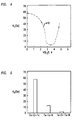
- FIG. 4 Shown in FIG. 4 is a plot 410 of magnetic coercivity of the inventive Fe-Cr-Ta-N films vs. nitrogen content (in volume %) in the Ar gas sputtering atmosphere.
- nitrogen content in the Fe-Cr-Ta-N films increases with the volume % of the nitrogen (N 2 ) gas in the sputtering atmosphere.
- the amount of nitrogen in the inventive alloy films is critical in determining the soft magnetic properties.
- the H c value of the inventive alloy films depend on the nitrogen content, with the lowest coercivity being obtained by sputtering at a nitrogen gas content of 3.5 volume %. Too low a nitrogen content is ineffective for preventing grain growth of an iron matrix and results in a high H c . Too high a nitrogen content reduces the saturation magnetization and also raises the H c . Thus, in order to achieve low H c , there appears to be an optimal range of nitrogen content for a given alloy composition.
- FIG. 5 Shown in FIG. 5 is a diagram comparing the magnetic softness in terms of H c in the as-deposited condition of Fe-Cr-Ta, Fe-Ta-N and Fe-Cr-Ta-N films having comparable compositions of alloying elements (if present, approximately 5% Cr, approximately 1% Ta, approximately 7% N and balance Fe) and comparable saturation moments.
- alloying elements if present, approximately 5% Cr, approximately 1% Ta, approximately 7% N and balance Fe
- FIG. 5 shows that the addition of Cr to Fe-Ta-N, as well as the addition of N to Fe-Cr-Ta, significantly improves the soft magnetic properties.
- the inventive films exhibit substantially improved (at least 50%) resistance to corrosion/oxidation as compared to the prior art soft magnetic films without Cr.
- films approximately 1000 ⁇ thick and having a composition of Fe-6.3% Cr-3.2%Ta-16.1%N on a Si substrate were kept in tap water or 50% nitric acid for 30 minutes. There was no noticeable corrosion or dissolution of the thin film material in either case. Also, there was no discoloration or decrease in film thickness, and there was no change in total magnetic moment. Furthermore, the H c and the "squareness" of the M-H loop also did not change.
- the resistance to oxidation is important in maintaining the soft magnetic properties during actual device usage, as the oxidation of Fe-rich alloys causes changes toward lower 4 ⁇ M s , higher coercivity and inferior permeability.
- the inventive films are given an optional low-temperature heat treatment, if desired, to further improve the soft magnetic properties.
- low heat treating temperatures below approximately 150°C are used.
- a high vacuum atmosphere e.g., better than approximately 10 -4 Torr
- a lower vacuum is used if the top surface of the film of film layers is protected, e.g., by oxidation-resistant coatings such as Cr, Al, oxide, or nitride films.
- an as-deposited film composition of Fe-4% Cr- 1.1% Ta-6% N was approximately 1500 ⁇ and exhibited a 4 ⁇ M s of approximately 15.1 kG and a H c of approximately 1.1 Oe.
- the film was heat treated at 125°C for approximately 3 hours in a vacuum of 10 -4 Torr, the resultant film exhibited an improved 4 ⁇ M s of approximately 20.2 kG and a H c of approximately 0.9 Oe.
- the film is formed as a composite structure with a different type of magnetic layer.
- the composite structure has one or more exchange bias films, which are antiferromagnetic, ferromagnetic or ferrimagnetic, added directly on the soft magnetic film surface.
- a thin film of Fe-50% manganese antiferromagnetic alloy is added onto some or all of the Fe-Cr-N based soft magnetic layers to shift the M-H loop (by more than the H c of the soft magnetic film, e.g., by at least 2 Oe) and to allow high frequency operation of the soft magnetic films in the internal bias-field mode with minimal magnetic domain wall motion.
- Step 140 comprises cutting up the substrate (containing a deposited and optionally patterned single layer, multilayer or composite-structured magnetic film) into a desirable size, adding appropriate interconnection and conductor circuitry if needed, and assembling within the desired electromagnetic devices.
- FIGS. 6a-b are schematic diagrams illustrating a pot-core type microtransformer design comprising the inventive Fe-Cr-N based films.
- the multiplicity of soft magnetic film layers 610 laminates with polyimide or other insulating layers therebetween
- a patterned conductor layer 620 e.g., containing Cu lines
- more magnetic film laminations 630 are deposited, as shown.
- FIGS. 7a-b are schematic diagrams illustrating a toroidal microtransformer design.
- a conductor layer 710 in the form of parallel segments is prepared first, then a Fe-Cr-N based magnetic film lamination 720 is deposited thereon, and then a top conductor layer 730 in the form of parallel segments is added to be connected with segments of conductor layer 710 to form a toroidal winding configuration.
- the Fe-Cr-N based films are deposited in such a way that the easy axis of magnetization coincides with the direction of applied field from the windings.
- magnetization switching by domain wall motion is not desirable and hence the magnetically hard direction is used so that coherent spin rotation mode is operational.
- uniaxial magnetic anisotrophy which is induced, e.g., by thin film deposition in the presence of magnetic fields, can be defined in terms of an anisotrophy field, H k , which is represented by the field in which the hard axis magnetization loop reaches saturation. See, for example, FIG. 3c.
- Desirable H k values in the inventive films are, e.g., in the range from 10-100 Oe and preferably in the range from 20-50 Oe. Too high of a H k value reduces the high frequency permeability (which is proportional to 4 ⁇ M/ H k in the hard axis operation). Too low of a H k value causes the ferromagnetic resonance frequency to be reduced and interfere with operating frequency ranges. Therefore, too much magnetic softness (i.e., a very low H k value) is undesirable for high frequency devices of this invention.
- the "squareness" of the M-H loop in the easy axis direction is desirable, as the film first can be saturated essentially into a single domain state along the easy axis, and then operated in a high frequency alternating current (AC) mode in the hard axis direction to minimize the domain wall motion.
- FIGS. 8a-b show embodiments of the invention incorporated into electromagnetic devices.
- a cross-sectional view of a recording read-write head comprising an embodiment of the inventive film is illustrated in FIG. 8a.
- the soft magnetic film 810 serves to amplify the magnetic signal from the recorded magnetic memory bit information in the magnetic disk or tape 820 so that the inductive sense coil or magnetoresistive sensor 830 can generate a higher output signal.
- the inventive film is used as the high-magnetization material in the metal-in-gap (MIG) type head configuration.
- the head 850 is made of, e.g., ferrite.
Landscapes
- Engineering & Computer Science (AREA)
- Power Engineering (AREA)
- Chemical & Material Sciences (AREA)
- Crystallography & Structural Chemistry (AREA)
- Nanotechnology (AREA)
- Manufacturing & Machinery (AREA)
- Physics & Mathematics (AREA)
- Materials Engineering (AREA)
- Microelectronics & Electronic Packaging (AREA)
- Inorganic Chemistry (AREA)
- Spectroscopy & Molecular Physics (AREA)
- Condensed Matter Physics & Semiconductors (AREA)
- General Physics & Mathematics (AREA)
- Thin Magnetic Films (AREA)
- Magnetic Heads (AREA)
Applications Claiming Priority (2)
| Application Number | Priority Date | Filing Date | Title |
|---|---|---|---|
| US595543 | 1996-02-02 | ||
| US08/595,543 US5780175A (en) | 1996-02-02 | 1996-02-02 | Articles comprising magnetically soft thin films and methods for making such articles |
Publications (1)
| Publication Number | Publication Date |
|---|---|
| EP0788120A1 true EP0788120A1 (de) | 1997-08-06 |
Family
ID=24383662
Family Applications (1)
| Application Number | Title | Priority Date | Filing Date |
|---|---|---|---|
| EP97300373A Ceased EP0788120A1 (de) | 1996-02-02 | 1997-01-21 | Gegenstände mit weichmagnetischen Dünnschichten und ihr Herstellungsverfahren |
Country Status (4)
| Country | Link |
|---|---|
| US (2) | US5780175A (de) |
| EP (1) | EP0788120A1 (de) |
| JP (2) | JP3677137B2 (de) |
| TW (1) | TW360884B (de) |
Families Citing this family (32)
| Publication number | Priority date | Publication date | Assignee | Title |
|---|---|---|---|---|
| US5772797A (en) * | 1989-01-26 | 1998-06-30 | Fuji Photo Film Co., Ltd. | Soft magnetic thin film, method for preparing same and magnetic head |
| JP2924785B2 (ja) * | 1996-04-25 | 1999-07-26 | 日本電気株式会社 | 磁気抵抗効果素子薄膜及びその製造方法 |
| JP4562818B2 (ja) * | 1997-02-14 | 2010-10-13 | パナソニック株式会社 | 人工格子多層膜の着膜装置 |
| US6376909B1 (en) | 1999-09-02 | 2002-04-23 | Micron Technology, Inc. | Mixed-mode stacked integrated circuit with power supply circuit part of the stack |
| US6856228B2 (en) * | 1999-11-23 | 2005-02-15 | Intel Corporation | Integrated inductor |
| US6891461B2 (en) | 1999-11-23 | 2005-05-10 | Intel Corporation | Integrated transformer |
| US6815220B2 (en) * | 1999-11-23 | 2004-11-09 | Intel Corporation | Magnetic layer processing |
| US6452247B1 (en) * | 1999-11-23 | 2002-09-17 | Intel Corporation | Inductor for integrated circuit |
| US6870456B2 (en) * | 1999-11-23 | 2005-03-22 | Intel Corporation | Integrated transformer |
| US6420954B1 (en) | 1999-12-10 | 2002-07-16 | Micron Technology, Inc. | Coupled multilayer soft magnetic films for high frequency microtransformer for system-on-chip power supply |
| US20020058159A1 (en) * | 2000-11-15 | 2002-05-16 | Yukiko Kubota | Soft magnetic underlayer (SUL) for perpendicular recording medium |
| JP4333900B2 (ja) * | 2000-11-30 | 2009-09-16 | エーエスエム インターナショナル エヌ.ヴェー. | 磁気メモリセル、磁気構造体及び磁気素子の製造方法、並びに磁気構造体用金属層の成長方法 |
| KR20020078705A (ko) * | 2001-04-09 | 2002-10-19 | 한국과학기술연구원 | FeTiN계 연자성 박막합금 조성물 |
| US6759081B2 (en) | 2001-05-11 | 2004-07-06 | Asm International, N.V. | Method of depositing thin films for magnetic heads |
| US6692619B1 (en) | 2001-08-14 | 2004-02-17 | Seagate Technology Llc | Sputtering target and method for making composite soft magnetic films |
| JP4720067B2 (ja) * | 2003-01-24 | 2011-07-13 | Tdk株式会社 | 磁気記憶セルおよび磁気メモリデバイスならびに磁気メモリデバイスの製造方法 |
| US7852185B2 (en) * | 2003-05-05 | 2010-12-14 | Intel Corporation | On-die micro-transformer structures with magnetic materials |
| JP2005332474A (ja) * | 2004-05-19 | 2005-12-02 | Hitachi Global Storage Technologies Netherlands Bv | 熱アシスト磁気記録装置 |
| US20060042938A1 (en) * | 2004-09-01 | 2006-03-02 | Heraeus, Inc. | Sputter target material for improved magnetic layer |
| US8134548B2 (en) | 2005-06-30 | 2012-03-13 | Micron Technology, Inc. | DC-DC converter switching transistor current measurement technique |
| JP4331182B2 (ja) * | 2006-04-14 | 2009-09-16 | 山陽特殊製鋼株式会社 | 軟磁性ターゲット材 |
| JP5037036B2 (ja) * | 2006-05-02 | 2012-09-26 | 山陽特殊製鋼株式会社 | FeCo系ターゲット材 |
| WO2007149135A2 (en) * | 2006-06-16 | 2007-12-27 | Ningbo Signatronic Technologies, Ltd. | Anti-theft security marker with soft magnetic bias component |
| CN100447911C (zh) * | 2006-06-16 | 2008-12-31 | 李霖 | 软磁材料偏置片的制造方法及使用该偏置片的防盗声磁标签 |
| JP4907259B2 (ja) * | 2006-08-16 | 2012-03-28 | 山陽特殊製鋼株式会社 | Crを添加したFeCoB系ターゲット材 |
| JP2008121071A (ja) * | 2006-11-13 | 2008-05-29 | Sanyo Special Steel Co Ltd | 軟磁性FeCo系ターゲット材 |
| JP5111835B2 (ja) * | 2006-11-17 | 2013-01-09 | 山陽特殊製鋼株式会社 | (CoFe)ZrNb/Ta/Hf系ターゲット材およびその製造方法 |
| JP5253781B2 (ja) * | 2007-09-18 | 2013-07-31 | 山陽特殊製鋼株式会社 | 垂直磁気記録媒体における軟磁性膜層用合金ターゲット材 |
| US8993073B2 (en) * | 2008-07-14 | 2015-03-31 | Seagate Technology Llc | Applying bias voltage during formation of granular recording media |
| DE102011086403A1 (de) | 2011-11-15 | 2013-05-16 | Würth Elektronik eiSos Gmbh & Co. KG | Induktionsbauteil |
| US11322290B2 (en) * | 2018-06-19 | 2022-05-03 | Intel Corporation | Techniques for an inductor at a first level interface |
| CN119296946B (zh) * | 2024-12-09 | 2025-03-04 | 包头方谷磁业有限责任公司 | 基于氧化铝掺杂的烧结钕铁硼磁体电阻率优化方法及系统 |
Citations (4)
| Publication number | Priority date | Publication date | Assignee | Title |
|---|---|---|---|---|
| EP0620571A2 (de) * | 1993-03-31 | 1994-10-19 | Matsushita Electric Industrial Co., Ltd. | Weichmagnetischer Mehrschichtfilm für einen Magnetkopf |
| JPH07122428A (ja) * | 1993-10-28 | 1995-05-12 | Matsushita Electric Ind Co Ltd | 磁性合金膜およびこれを用いた磁気ヘッド |
| JPH07130538A (ja) * | 1993-11-01 | 1995-05-19 | Hitachi Metals Ltd | 磁性合金膜および磁気ヘッド |
| US5421915A (en) * | 1989-01-26 | 1995-06-06 | Fuji Photo Film Co., Ltd. | Method for preparing same and magnetic head |
Family Cites Families (2)
| Publication number | Priority date | Publication date | Assignee | Title |
|---|---|---|---|---|
| US4835069A (en) * | 1983-08-06 | 1989-05-30 | Canon Kabushiki Kaisha | Magnetic recording medium |
| US5262915A (en) * | 1990-08-23 | 1993-11-16 | Tdk Corporation | Magnetic head comprising a soft magnetic thin film of FeNiZrN having enhanced (100) orientation |
-
1996
- 1996-02-02 US US08/595,543 patent/US5780175A/en not_active Expired - Lifetime
-
1997
- 1997-01-21 EP EP97300373A patent/EP0788120A1/de not_active Ceased
- 1997-01-21 TW TW086100615A patent/TW360884B/zh not_active IP Right Cessation
- 1997-02-03 JP JP02025397A patent/JP3677137B2/ja not_active Expired - Lifetime
- 1997-02-03 JP JP9020254A patent/JPH09320846A/ja active Pending
- 1997-11-06 US US08/965,682 patent/US5976715A/en not_active Expired - Fee Related
Patent Citations (4)
| Publication number | Priority date | Publication date | Assignee | Title |
|---|---|---|---|---|
| US5421915A (en) * | 1989-01-26 | 1995-06-06 | Fuji Photo Film Co., Ltd. | Method for preparing same and magnetic head |
| EP0620571A2 (de) * | 1993-03-31 | 1994-10-19 | Matsushita Electric Industrial Co., Ltd. | Weichmagnetischer Mehrschichtfilm für einen Magnetkopf |
| JPH07122428A (ja) * | 1993-10-28 | 1995-05-12 | Matsushita Electric Ind Co Ltd | 磁性合金膜およびこれを用いた磁気ヘッド |
| JPH07130538A (ja) * | 1993-11-01 | 1995-05-19 | Hitachi Metals Ltd | 磁性合金膜および磁気ヘッド |
Non-Patent Citations (1)
| Title |
|---|
| PATENT ABSTRACTS OF JAPAN vol. 095, no. 008 29 September 1995 (1995-09-29) * |
Also Published As
| Publication number | Publication date |
|---|---|
| JPH09237412A (ja) | 1997-09-09 |
| US5780175A (en) | 1998-07-14 |
| TW360884B (en) | 1999-06-11 |
| US5976715A (en) | 1999-11-02 |
| JPH09320846A (ja) | 1997-12-12 |
| JP3677137B2 (ja) | 2005-07-27 |
Similar Documents
| Publication | Publication Date | Title |
|---|---|---|
| US5780175A (en) | Articles comprising magnetically soft thin films and methods for making such articles | |
| US5998048A (en) | Article comprising anisotropic Co-Fe-Cr-N soft magnetic thin films | |
| Ohnuma et al. | Magnetostriction and soft magnetic properties of (Co 1− x Fe x)–Al–O granular films with high electrical resistivity | |
| US7369027B2 (en) | High frequency magnetic thin film, composite magnetic thin film and magnetic device using them | |
| US5484491A (en) | Ferromagnetic film | |
| US5661449A (en) | Magnetic multilayer film, method for making, and magnetoresistance device | |
| US8133332B2 (en) | Method for preparing FePt media at low ordering temperature and fabrication of exchange coupled composite media and gradient anisotropy media for magnetic recording | |
| US6841259B1 (en) | Magnetic thin film, production method therefor, evaluation method therefor and magnetic head using it, magnetic recording device and magnetic device | |
| Kohmoto | Recent development of thin film materials for magnetic heads | |
| JPWO2001093286A1 (ja) | 磁性薄膜、その製造方法、その評価方法及びこれを用いた磁気ヘッド、磁気記録装置並びに磁気デバイス | |
| US5716719A (en) | Magnetoresistance effect element | |
| US20020064689A1 (en) | Magnetic recording medium and magnetic recording apparatus | |
| US6171716B1 (en) | Soft magnetic film, and thin film magnetic head, planer magnetic element, and filter using the soft magnetic film | |
| Katada et al. | Soft magnetic properties and microstructure of NiFe (Cr)/FeCo/NiFe (Cr) films with large saturation magnetization | |
| Kataoka et al. | High frequency permeability of nanocrystalline Fe–Cu–Nb–Si–B single and multilayer films | |
| KR20050084458A (ko) | 고주파용 자성박막, 복합자성박막 및 이것을 사용한자기소자 | |
| JP3655031B2 (ja) | 磁気抵抗効果素子および磁気再生システム | |
| EP0766272B1 (de) | Dünne magnetische Filme und ihre Verwendungen in Magnetdünnschichtelementen | |
| US5413868A (en) | Perpendicular magnetic recording medium comprising a magnetic thin film of cobalt, palladium, chromium and oxygen | |
| JP2704157B2 (ja) | 磁性部品 | |
| JP3691920B2 (ja) | 磁気抵抗効果素子および磁気再生システム | |
| JPH07235034A (ja) | 垂直磁気記録媒体および磁気記録再生装置 | |
| JPH0282601A (ja) | 多層磁性膜 | |
| Cates et al. | Magnetostriction in FeTaN thin films | |
| Roozeboom et al. | Rapid Thermal Magnetic Annealing: A Novel Technique in Thin-Film Recording Head Production? |
Legal Events
| Date | Code | Title | Description |
|---|---|---|---|
| PUAI | Public reference made under article 153(3) epc to a published international application that has entered the european phase |
Free format text: ORIGINAL CODE: 0009012 |
|
| AK | Designated contracting states |
Kind code of ref document: A1 Designated state(s): DE FR GB |
|
| 17P | Request for examination filed |
Effective date: 19980126 |
|
| 17Q | First examination report despatched |
Effective date: 19990811 |
|
| GRAG | Despatch of communication of intention to grant |
Free format text: ORIGINAL CODE: EPIDOS AGRA |
|
| STAA | Information on the status of an ep patent application or granted ep patent |
Free format text: STATUS: THE APPLICATION HAS BEEN REFUSED |
|
| 18R | Application refused |
Effective date: 20020826 |