EP0788154A2 - Elektronisches Schaltungssubstrat - Google Patents
Elektronisches Schaltungssubstrat Download PDFInfo
- Publication number
- EP0788154A2 EP0788154A2 EP97300488A EP97300488A EP0788154A2 EP 0788154 A2 EP0788154 A2 EP 0788154A2 EP 97300488 A EP97300488 A EP 97300488A EP 97300488 A EP97300488 A EP 97300488A EP 0788154 A2 EP0788154 A2 EP 0788154A2
- Authority
- EP
- European Patent Office
- Prior art keywords
- electronic circuit
- thermoplastic resin
- substrate
- resin
- circuit substrate
- Prior art date
- Legal status (The legal status is an assumption and is not a legal conclusion. Google has not performed a legal analysis and makes no representation as to the accuracy of the status listed.)
- Withdrawn
Links
Images

Classifications
-
- H—ELECTRICITY
- H10—SEMICONDUCTOR DEVICES; ELECTRIC SOLID-STATE DEVICES NOT OTHERWISE PROVIDED FOR
- H10W—GENERIC PACKAGES, INTERCONNECTIONS, CONNECTORS OR OTHER CONSTRUCTIONAL DETAILS OF DEVICES COVERED BY CLASS H10
- H10W74/00—Encapsulations, e.g. protective coatings
- H10W74/40—Encapsulations, e.g. protective coatings characterised by their materials
- H10W74/47—Encapsulations, e.g. protective coatings characterised by their materials comprising organic materials, e.g. plastics or resins
- H10W74/473—Encapsulations, e.g. protective coatings characterised by their materials comprising organic materials, e.g. plastics or resins containing a filler
-
- H—ELECTRICITY
- H05—ELECTRIC TECHNIQUES NOT OTHERWISE PROVIDED FOR
- H05K—PRINTED CIRCUITS; CASINGS OR CONSTRUCTIONAL DETAILS OF ELECTRIC APPARATUS; MANUFACTURE OF ASSEMBLAGES OF ELECTRICAL COMPONENTS
- H05K3/00—Apparatus or processes for manufacturing printed circuits
- H05K3/22—Secondary treatment of printed circuits
- H05K3/28—Applying non-metallic protective coatings
- H05K3/284—Applying non-metallic protective coatings for encapsulating mounted components
-
- C—CHEMISTRY; METALLURGY
- C09—DYES; PAINTS; POLISHES; NATURAL RESINS; ADHESIVES; COMPOSITIONS NOT OTHERWISE PROVIDED FOR; APPLICATIONS OF MATERIALS NOT OTHERWISE PROVIDED FOR
- C09K—MATERIALS FOR MISCELLANEOUS APPLICATIONS, NOT PROVIDED FOR ELSEWHERE
- C09K2323/00—Functional layers of liquid crystal optical display excluding electroactive liquid crystal layer characterised by chemical composition
- C09K2323/05—Bonding or intermediate layer characterised by chemical composition, e.g. sealant or spacer
- C09K2323/051—Inorganic, e.g. glass or silicon oxide
-
- Y—GENERAL TAGGING OF NEW TECHNOLOGICAL DEVELOPMENTS; GENERAL TAGGING OF CROSS-SECTIONAL TECHNOLOGIES SPANNING OVER SEVERAL SECTIONS OF THE IPC; TECHNICAL SUBJECTS COVERED BY FORMER USPC CROSS-REFERENCE ART COLLECTIONS [XRACs] AND DIGESTS
- Y10—TECHNICAL SUBJECTS COVERED BY FORMER USPC
- Y10T—TECHNICAL SUBJECTS COVERED BY FORMER US CLASSIFICATION
- Y10T428/00—Stock material or miscellaneous articles
- Y10T428/23—Sheet including cover or casing
-
- Y—GENERAL TAGGING OF NEW TECHNOLOGICAL DEVELOPMENTS; GENERAL TAGGING OF CROSS-SECTIONAL TECHNOLOGIES SPANNING OVER SEVERAL SECTIONS OF THE IPC; TECHNICAL SUBJECTS COVERED BY FORMER USPC CROSS-REFERENCE ART COLLECTIONS [XRACs] AND DIGESTS
- Y10—TECHNICAL SUBJECTS COVERED BY FORMER USPC
- Y10T—TECHNICAL SUBJECTS COVERED BY FORMER US CLASSIFICATION
- Y10T428/00—Stock material or miscellaneous articles
- Y10T428/23—Sheet including cover or casing
- Y10T428/232—Encased layer derived from inorganic settable ingredient
-
- Y—GENERAL TAGGING OF NEW TECHNOLOGICAL DEVELOPMENTS; GENERAL TAGGING OF CROSS-SECTIONAL TECHNOLOGIES SPANNING OVER SEVERAL SECTIONS OF THE IPC; TECHNICAL SUBJECTS COVERED BY FORMER USPC CROSS-REFERENCE ART COLLECTIONS [XRACs] AND DIGESTS
- Y10—TECHNICAL SUBJECTS COVERED BY FORMER USPC
- Y10T—TECHNICAL SUBJECTS COVERED BY FORMER US CLASSIFICATION
- Y10T428/00—Stock material or miscellaneous articles
- Y10T428/23—Sheet including cover or casing
- Y10T428/239—Complete cover or casing
-
- Y—GENERAL TAGGING OF NEW TECHNOLOGICAL DEVELOPMENTS; GENERAL TAGGING OF CROSS-SECTIONAL TECHNOLOGIES SPANNING OVER SEVERAL SECTIONS OF THE IPC; TECHNICAL SUBJECTS COVERED BY FORMER USPC CROSS-REFERENCE ART COLLECTIONS [XRACs] AND DIGESTS
- Y10—TECHNICAL SUBJECTS COVERED BY FORMER USPC
- Y10T—TECHNICAL SUBJECTS COVERED BY FORMER US CLASSIFICATION
- Y10T428/00—Stock material or miscellaneous articles
- Y10T428/25—Web or sheet containing structurally defined element or component and including a second component containing structurally defined particles
-
- Y—GENERAL TAGGING OF NEW TECHNOLOGICAL DEVELOPMENTS; GENERAL TAGGING OF CROSS-SECTIONAL TECHNOLOGIES SPANNING OVER SEVERAL SECTIONS OF THE IPC; TECHNICAL SUBJECTS COVERED BY FORMER USPC CROSS-REFERENCE ART COLLECTIONS [XRACs] AND DIGESTS
- Y10—TECHNICAL SUBJECTS COVERED BY FORMER USPC
- Y10T—TECHNICAL SUBJECTS COVERED BY FORMER US CLASSIFICATION
- Y10T428/00—Stock material or miscellaneous articles
- Y10T428/25—Web or sheet containing structurally defined element or component and including a second component containing structurally defined particles
- Y10T428/251—Mica
-
- Y—GENERAL TAGGING OF NEW TECHNOLOGICAL DEVELOPMENTS; GENERAL TAGGING OF CROSS-SECTIONAL TECHNOLOGIES SPANNING OVER SEVERAL SECTIONS OF THE IPC; TECHNICAL SUBJECTS COVERED BY FORMER USPC CROSS-REFERENCE ART COLLECTIONS [XRACs] AND DIGESTS
- Y10—TECHNICAL SUBJECTS COVERED BY FORMER USPC
- Y10T—TECHNICAL SUBJECTS COVERED BY FORMER US CLASSIFICATION
- Y10T428/00—Stock material or miscellaneous articles
- Y10T428/25—Web or sheet containing structurally defined element or component and including a second component containing structurally defined particles
- Y10T428/252—Glass or ceramic [i.e., fired or glazed clay, cement, etc.] [porcelain, quartz, etc.]
-
- Y—GENERAL TAGGING OF NEW TECHNOLOGICAL DEVELOPMENTS; GENERAL TAGGING OF CROSS-SECTIONAL TECHNOLOGIES SPANNING OVER SEVERAL SECTIONS OF THE IPC; TECHNICAL SUBJECTS COVERED BY FORMER USPC CROSS-REFERENCE ART COLLECTIONS [XRACs] AND DIGESTS
- Y10—TECHNICAL SUBJECTS COVERED BY FORMER USPC
- Y10T—TECHNICAL SUBJECTS COVERED BY FORMER US CLASSIFICATION
- Y10T428/00—Stock material or miscellaneous articles
- Y10T428/25—Web or sheet containing structurally defined element or component and including a second component containing structurally defined particles
- Y10T428/256—Heavy metal or aluminum or compound thereof
- Y10T428/257—Iron oxide or aluminum oxide
Definitions
- the present invention relates to an electronic circuit substrate sealed by resin.
- An electronic circuit substrate incorporated in a device used in an outdoor environment is usually sealed with resin or the like as it is often exposed to a severe condition under an extremely high or low temperature and/or with high humidity.
- the substrate is usually sealed by a conventional method requiring a long time, wherein the resin is provided to the substrate under a state of liquid for coating the whole surface or the surface of a specific component of the substrate and solidified.
- the sealing resin thereby enables a use of the substrate under a severe external condition.
- Fig. 2 is a sectional view of a circuit substrate sealed with a thermosetting resin by a conventional method.
- the reference numeral 1 designates a ceramic substrate
- 2 represents a mounted package component
- 3 represents a mounted chip component
- 4 represents a phenol resin used for sealing.
- the substrate 1 mounted with the components 2, 3 is dipped into the liquid phenol resin 4, and heated to solidify the resin 4.
- Fig. 3 is a sectional view of a substrate sealed by injection moulding using a conventional thermoplastic resin.
- the reference numeral 5 designates a ceramic substrate
- 6 represents a mounted package component
- 7 represents a mounted chip component
- 8 represents a thermoplastic resin used for sealing.
- the substrate 5 mounted with the components 6, 7 is set inside a metal mould of an injection moulding device, and the thermoplastic resin 8 is injected thereto and then solidified.
- the second conventional method described above wherein a thermoplastic resin is injected by an injection moulding device and solidified, requires less time for setting by application of thermoplastic resin.
- This method also facilitates introduction of an automatic assembly system due to more precise dimensions of the sealing resin formed by a metal mould. Since an engineering plastic has a high sealing effect, it is often used as a thermoplastic resin in this method. However, there is a great difference in the rate of thermal expansion (linear expansion coefficient) between the engineering plastic and the ceramic substrate. Under a certain condition such as a heat cycle test or the like, the shrinking resin sometimes causes cracks on the ceramic substrate, leading to a decrease in productivity of the electronic circuit substrate.
- the heat cycle test is, for example, carried out within the range from -40°C to +150°C depending on each case.
- a primary aim of the present invention is to overcome the above described conventional problems and to provide a ceramic substrate sealed with a thermoplastic engineering plastic with a high sealing effect which can be produced efficiently at a stable rate.
- an electronic circuit substrate of the present invention is sealed with a thermoplastic resin, the thermal-expansion coefficient of which is made to be close to that of a substrate made of ceramic by mixing a compound filler in the thermoplastic resin.
- the compound filler in the resin includes preferably at least two of milled fiber, glass fiber and flaked filler, and the amount of the compound filler in the resin is 50% and below in weight with respect to the resin.
- the thermoplastic resin consists preferably of liquid crystal polymer or of polyphenylenesulphide.
- the thermal-expansion coefficient of a thermoplastic resin used as a sealing material can be decreased to come nearer to the thermal expansion coefficient of a ceramic substrate by mixing fillers dispersedly in the resin.
- the difference can be considerably reduced by compounding fillers in the resin. The substrate is thus not stressed despite changes in ambient temperature, and cracks can be prevented.
- the electronic circuit substrate of the present invention allows for a stable use owing to the prevention of cracks.
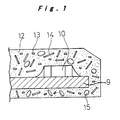
- Fig. 1 is a typified sketch of an electronic circuit substrate according to an embodiment of the present invention.
- the reference numeral 9 designates a ceramic substrate, on which a chip component 10 and a package component (not shown) are mounted.
- the numeral 12 represents a thermoplastic resin for sealing, and milled fiber 13, glass fiber 14, and flaked filler 15 are dispersedly added to the resin 12.
- Milled fiber 13 is made from longer glass fiber by cutting into pieces of medium length.
- the plasticity of the thermoplastic resin 12 is enhanced by adding this shorter milled fiber 13 compared with the resin with only the long glass fiber 14.
- the flaked filler 15 is made by forming metal oxide or the like into flakes.
- any combinations of the two out of the above mentioned three fillers will effect similarly. That is to say, only the milled fiber 13 and the glass fiber 14 can be added as well as only the glass fiber 14 and the flaked filler 15 or the flaked filler 15 and the milled fiber 13.
- the gross weight of the compound filler should be 50% and below with respect to the thermoplastic resin 12 from the standpoint of plasticity, and should be 20% and over with respect to the thermoplastic resin 12, from the standpoint of thermal-expansion coefficient.
- Liquid crystal polymer is most preferably used as the thermoplastic resin 12.
- Liquid crystal polymer is suitable for sealing as it has high heat resistance (more than 300°C of melting point), a low thermal-expansion coefficient and a low forming contraction coefficient.
- an aromatic liquid crystal polyester may be exemplarily used.
- Polyphenylenesulphide may be second most suitable as the thermoplastic resin 12, since it has various characteristics similar to those of liquid crystal polymer which are considered to be necessary as a proper sealing material.
- the sealing material was composed of aromatic liquid crystal polyester as a thermoplastic resin and of a compound filler dispersedly mixed therein.
- the filler consisted of glass fiber, milled fiber and flaked filler.
- the milled fiber was made from glass fiber cut into pieces by a milling of length from one fifth to one tenth with respect to raw fiber.
- metal oxide such as zinc oxide or the like was employed.
- the milled fiber, the glass fiber and the flaked filler were mixed at the rates of 15%, 20% and 5% in weight, respectively, in relation to the whole amount of the liquid crystal polymer.
- the thermal-expansion coefficient of the sealing material composed as described above was 0.9 ⁇ 10 -5 /°C, which is quite close to the thermal-expansion coefficient 0.7 ⁇ 10 -5 /°C of a ceramic substrate generally used.
- An electronic circuit substrate comprising the ceramic substrate was set in a metal mould of an injection moulding device.
- the above described sealing material was then injected thereinto and solidified, sealing the whole surface of the electronic circuit substrate as shown in Fig. 1.
- the thermal-expansion coefficient of the sealing material can be made close to that of the ceramic substrate by mixing the compound filler in the sealing material.
- the electronic circuit substrate of the present invention is thus stress resistant and does not crack despite changes in external temperature. Since the substrate is sealed by injection moulding using a metal mould, the time required for processing is reduced, and an automatic assembly system can be introduced owing to the precise dimensions of the sealed substrate.
Landscapes
- Engineering & Computer Science (AREA)
- Manufacturing & Machinery (AREA)
- Microelectronics & Electronic Packaging (AREA)
- Structures Or Materials For Encapsulating Or Coating Semiconductor Devices Or Solid State Devices (AREA)
- Non-Metallic Protective Coatings For Printed Circuits (AREA)
- Compositions Of Macromolecular Compounds (AREA)
Applications Claiming Priority (2)
| Application Number | Priority Date | Filing Date | Title |
|---|---|---|---|
| JP8013966A JPH09214111A (ja) | 1996-01-30 | 1996-01-30 | 電子回路基板 |
| JP13966/96 | 1996-01-30 |
Publications (2)
| Publication Number | Publication Date |
|---|---|
| EP0788154A2 true EP0788154A2 (de) | 1997-08-06 |
| EP0788154A3 EP0788154A3 (de) | 1998-08-05 |
Family
ID=11847968
Family Applications (1)
| Application Number | Title | Priority Date | Filing Date |
|---|---|---|---|
| EP97300488A Withdrawn EP0788154A3 (de) | 1996-01-30 | 1997-01-27 | Elektronisches Schaltungssubstrat |
Country Status (3)
| Country | Link |
|---|---|
| US (1) | US5858481A (de) |
| EP (1) | EP0788154A3 (de) |
| JP (1) | JPH09214111A (de) |
Families Citing this family (6)
| Publication number | Priority date | Publication date | Assignee | Title |
|---|---|---|---|---|
| US20020167804A1 (en) * | 2001-05-14 | 2002-11-14 | Intel Corporation | Polymeric encapsulation material with fibrous filler for use in microelectronic circuit packaging |
| US8023071B2 (en) * | 2002-11-25 | 2011-09-20 | Sipix Imaging, Inc. | Transmissive or reflective liquid crystal display |
| TWI457835B (zh) * | 2004-02-04 | 2014-10-21 | Semiconductor Energy Lab | 攜帶薄膜積體電路的物品 |
| KR100745316B1 (ko) * | 2006-07-11 | 2007-08-01 | 삼성전자주식회사 | 고강도 유리섬유의 제조방법 및 이에 의해 제조된 고강도유리섬유를 포함하는 기판 |
| USD764424S1 (en) | 2014-05-15 | 2016-08-23 | Kabushiki Kaisha Toshiba | Substrate for an electronic circuit |
| CN110944275B (zh) * | 2019-12-31 | 2025-02-18 | 潍坊歌尔微电子有限公司 | 防尘结构、麦克风封装结构以及电子设备 |
Family Cites Families (9)
| Publication number | Priority date | Publication date | Assignee | Title |
|---|---|---|---|---|
| US4453903A (en) * | 1981-04-15 | 1984-06-12 | North American Philips Corporation | Insert molding gate design for encapsulating electronic ceramics with thermoplastic materials |
| JPS62108557A (ja) * | 1985-11-06 | 1987-05-19 | Hitachi Tobu Semiconductor Ltd | モ−ルド品およびその製造方法 |
| EP0340492A3 (de) * | 1988-05-02 | 1990-07-04 | International Business Machines Corporation | Konforme Versieglung und interplanare Verkapselung elektronischer Anordnungsstrukturen |
| JPH0768437B2 (ja) * | 1988-11-28 | 1995-07-26 | 三菱化学株式会社 | 樹脂組成物 |
| JP2830279B2 (ja) * | 1989-05-11 | 1998-12-02 | 住友化学工業株式会社 | 流動性の改良された液晶ポリエステル樹脂組成物 |
| US5070127A (en) * | 1989-07-07 | 1991-12-03 | Hoechst Celanese Corporation | Impact modified polyphenylene sulfide |
| JPH07118420B2 (ja) * | 1989-09-08 | 1995-12-18 | 松下電器産業株式会社 | コイル部品 |
| JP3048650B2 (ja) * | 1990-12-28 | 2000-06-05 | 京セラ株式会社 | 電子部品用封止材及びそれを用いた電子部品 |
| JPH088354A (ja) * | 1994-06-17 | 1996-01-12 | Hitachi Ltd | 半導体装置およびその製法 |
-
1996
- 1996-01-30 JP JP8013966A patent/JPH09214111A/ja active Pending
-
1997
- 1997-01-27 EP EP97300488A patent/EP0788154A3/de not_active Withdrawn
- 1997-01-30 US US08/791,132 patent/US5858481A/en not_active Expired - Fee Related
Also Published As
| Publication number | Publication date |
|---|---|
| US5858481A (en) | 1999-01-12 |
| EP0788154A3 (de) | 1998-08-05 |
| JPH09214111A (ja) | 1997-08-15 |
Similar Documents
| Publication | Publication Date | Title |
|---|---|---|
| US4190855A (en) | Installation of a semiconductor chip on a glass substrate | |
| US8853313B2 (en) | Thermally conductive polymer compositions having low thermal expansion characteristics | |
| EP0044136B1 (de) | Einkapselung einer elektronischen Vorrichtung | |
| US5909915A (en) | Resin-molded electronic circuit device | |
| US5043211A (en) | Epoxy resin composition and a resin-sealed semiconductor device | |
| US6311769B1 (en) | Thermal interface materials using thermally conductive fiber and polymer matrix materials | |
| CA1265260A (en) | Method of sealing electric and electronic parts | |
| EP0867475A3 (de) | Epoxidharzzusammensetzung geeignet zur Verkapselung von Halbleiteranordnungen und harzverkapselte Halbleiteranordnungen | |
| US5904505A (en) | Process for producing encapsulated semiconductor device having metal foil material covering and metal foil | |
| US5858481A (en) | Electronic circuit substrate | |
| KR100896858B1 (ko) | 에폭시 수지 조성물 및 반도체 장치 | |
| WO1999033106A1 (de) | Kunststoffverbundkörper | |
| US4029628A (en) | Bonding material for planar electronic device | |
| JPS6136710B2 (de) | ||
| KR100349406B1 (ko) | 반도체장치의제법및그에사용되는밀봉용펠릿 | |
| US6052893A (en) | Process for manufacturing a resin-encapsulated electronic product | |
| WO2001006442A2 (en) | Carrier tray for integrated circuits such as microprocessors | |
| GB1186075A (en) | Improvements in and relating to Methods of Manufacturing Layers of Grains for Electrical Devices | |
| CN1324699C (zh) | 功率半导体模块 | |
| US6506328B1 (en) | Process for producing an electronic component | |
| JPH0588847B2 (de) | ||
| US7119449B2 (en) | Enhancement of underfill physical properties by the addition of thermotropic cellulose | |
| KR0158716B1 (ko) | 광반도체용 에폭시 수지조성물 | |
| JP2002275358A (ja) | エポキシ系樹脂組成物および半導体装置 | |
| JPS5967637A (ja) | 半導体素子の製造方法 |
Legal Events
| Date | Code | Title | Description |
|---|---|---|---|
| PUAI | Public reference made under article 153(3) epc to a published international application that has entered the european phase |
Free format text: ORIGINAL CODE: 0009012 |
|
| AK | Designated contracting states |
Kind code of ref document: A2 Designated state(s): DE FR GB |
|
| PUAL | Search report despatched |
Free format text: ORIGINAL CODE: 0009013 |
|
| AK | Designated contracting states |
Kind code of ref document: A3 Designated state(s): DE FR GB |
|
| 17P | Request for examination filed |
Effective date: 19981201 |
|
| 17Q | First examination report despatched |
Effective date: 20020717 |
|
| STAA | Information on the status of an ep patent application or granted ep patent |
Free format text: STATUS: THE APPLICATION IS DEEMED TO BE WITHDRAWN |
|
| 18D | Application deemed to be withdrawn |
Effective date: 20021128 |