EP0788229A2 - Spitzenwertermittlungsgerät - Google Patents
Spitzenwertermittlungsgerät Download PDFInfo
- Publication number
- EP0788229A2 EP0788229A2 EP97300558A EP97300558A EP0788229A2 EP 0788229 A2 EP0788229 A2 EP 0788229A2 EP 97300558 A EP97300558 A EP 97300558A EP 97300558 A EP97300558 A EP 97300558A EP 0788229 A2 EP0788229 A2 EP 0788229A2
- Authority
- EP
- European Patent Office
- Prior art keywords
- signal
- buffer means
- output
- detecting apparatus
- peak detecting
- Prior art date
- Legal status (The legal status is an assumption and is not a legal conclusion. Google has not performed a legal analysis and makes no representation as to the accuracy of the status listed.)
- Granted
Links
- 239000003990 capacitor Substances 0.000 claims description 44
- 230000007423 decrease Effects 0.000 abstract description 2
- 238000010586 diagram Methods 0.000 description 16
- 238000001514 detection method Methods 0.000 description 8
- 238000010276 construction Methods 0.000 description 2
- 238000007796 conventional method Methods 0.000 description 1
- 230000014509 gene expression Effects 0.000 description 1
- 238000000034 method Methods 0.000 description 1
- 229920006395 saturated elastomer Polymers 0.000 description 1
Images


Classifications
-
- G—PHYSICS
- G01—MEASURING; TESTING
- G01R—MEASURING ELECTRIC VARIABLES; MEASURING MAGNETIC VARIABLES
- G01R19/00—Arrangements for measuring currents or voltages or for indicating presence or sign thereof
- G01R19/04—Measuring peak values or amplitude or envelope of AC or of pulses
Definitions
- the invention relates to a peak detecting apparatus and, more particularly, to a peak detecting apparatus for detecting peak values of signals from a plurality of signal sources.
- IN 1 to IN 3 denote input terminals which are connected to signal sources.
- the input terminals are connected to holding capacitors CT 1 to CT 3 and Darlington type emitter-follower circuits Q 11 •Q 21 •M 31 to Q 13 •Q 23 •M 33 , which are buffer means, through switching means M 21 to M 23 , respectively.
- M 11 to M 13 denote reset means.
- Output sides of the buffer means are commonly connected and output signals are increased by proper gain times by an amplifier A 1 and are outputted.
- a first peak detecting apparatus comprising: a plurality of first buffer means to each of which a signal is inputted; a plurality of second buffer means connected to the plurality of first buffer means; and a common output line for commonly connecting output sides of the plurality of second buffer means.
- a second peak detecting apparatus in which the plurality of first buffer means are constructed by emitter-follower circuits.
- a third peak detecting apparatus comprising a dummy output unit having the first buffer means which are connected to a voltage source and the second buffer means which are connected to the first buffer means, wherein a difference between an output from the common output line and an output from the dummy output unit is processed.
- a fourth peak detecting apparatus in which a capacitor is serially connected to an input side of each of the first buffer means to which the signals are inputted and reset means are connected between the input sides of the first buffer means and the capacitors.
- a fifth peak detecting apparatus in which reset means are provided on input sides of the first buffer means to which the signals are inputted and difference processing means for removing an electric potential of the common output line which was raised by a reset potential of the reset means is provided on the output side of the dummy output unit.
- a sixth peak detecting apparatus comprising: clamping means for clamping the signal that is outputted from the common output line; and comparing means for comparing a signal voltage from the clamping means and a reference voltage.
- a peak detection incorporates not only a maximum value detection but also a minimum value detection.
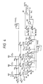
- Fig. 1 is a circuit constructional diagram showing the first embodiment of a peak detecting apparatus of the invention.
- the embodiment relates to the peak detecting apparatus having three signal input terminals IN 1 to IN 3 . Those input terminals are connected to the holding capacitors CT 1 to CT 3 and the Darlington type emitter-follower circuits Q 11 •Q 21 •M 31 to Q 13 •Q 23 •M 33 , which are first buffer means, through the switching means M 21 to M 23 , respectively.
- M 11 • to M 13 denote the reset means connected to a reset voltage source (voltage v CL ).
- the output sides of the first buffer means are connected to bases of NPN transistors Q 31 to Q 33 as second buffer means. Emitters of the NPN transistors Q 31 to Q 33 are commonly connected and a common emitter output is increased by proper gain times by the amplifier A 1 and is outputted.
- M 41 denotes reset means connected to a predetermined voltage source (GND here).
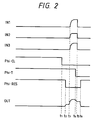
- a terminal Phi-CL is set to the high (H) level until time t 1 , thereby making the reset means M 11 to M 13 conductive and resetting the holding capacitors CT 1 to CT 3 to the voltage V CL (in this instance, a terminal Phi-T is also set to the H level and the switching means M 21 to M 23 are made conductive).
- a terminal Phi-RES is set to the H level and the common output line also maintains a predetermined reset potential.
- base potentials of the NPN transistors Q 31 to Q 33 serving as second buffer means depend on a magnitude of the signal from each signal source, when the electric potential of the common output line rises, the transistors other than the transistor to which the signal at the peak level was inputted is made nonconductive due to a drop of a base-emitter voltage.
- the terminal Phi-T is reduced from the H level to the L level, the switching means M 21 to M 23 are made nonconductive, and their signals are held in the holding capacitors CT 1 to CT 3 , respectively.
- the signals trail at time t 5 .
- the terminal Phi-RES is raised from the L level to the H level and the common output line is reset.
- the peak voltage of the signal from each signal source can be accurately generated from the amplifier A 1 connected to the common output line.
- the common output line is not directly connected to the first buffer means because it is connected to the first buffer means through the second buffer means. Even if the number of signal sources for outputting the peak values changes, a situation such that the output values differ as in the conventional peak detecting apparatus shown in Fig. 10 doesn't occur.
- the gain is set to a high value of tens of times or more or in case of forming the reference power source V ref in an IC or the like, there is a case where input/output ranges of the amplifier A 1 largely fluctuate due to a variation or the like of the device.
- the second embodiment can solve such a problem.
- Fig. 3 is a circuit constructional diagram showing the second embodiment of a peak detecting apparatus of the invention.
- a dummy output unit is further added to the circuit connected to the three signal input terminals IN 1 to IN 3 in the embodiment shown in Fig. 1, thereby generating a differential signal as an output between the peak value of the three input signals and a dummy signal.
- one terminal of switching means M 24 is connected to the reset power source (voltage V CL ) and another terminal is connected to a holding capacitor CT 4 and a Darlington type emitter-follower circuit Q 14 •Q 24 •M 34 which are first buffer means.
- An output side of the first buffer means is connected to a base of an NPN transistor Q 34 as second buffer means.
- An emitter of the NPN transistor Q 34 is connected to an output line other than the common output line and is connected to an amplifier A 2 .
- a reference power source V connected to the amplifier A 2 in the embodiment of Fig. 1 is replaced by an output voltage from the dummy output unit and the other component elements are similar to those of the peak detecting apparatus of the embodiment of Fig. 1.
- Conducting and nonconducting operations of the switching means M 24 are controlled in a manner similar to the switching means M 21 to M 23 and a terminal Phi-RES2 is set to the H level. Since the terminal Phi-RES2 is now set to the H level, switching means M 42 is always conducting and a variation in characteristics of a DC level is eliminated. However, the variation in characteristics can be also eliminated by making the terminal Phi-RES2 nonconductive as necessary.
- the characteristics variation of each device can be autonomously corrected and the stable output DC level can be derived.
- Fig. 4 is a circuit constructional diagram showing the third embodiment of a peak detecting apparatus of the invention.
- a capacitor is added to each signal input line of the peak detecting apparatus of the embodiment shown in Fig. 3 and when two signals are time-sequentially inputted from signal sources to an input terminal, a difference between those signals is processed and a peak of a differential signal is generated. It will be obviously understood that a process to add the capacitor to each signal input line can be also performed to the peak detecting apparatus in the embodiment shown in Fig. 1.
- capacitors CC 1 to CC 3 are connected to the signal input terminals IN 1 to IN 3 .
- a differential processing operation will now be described hereinbelow on the assumption that two signals are time-sequentially inputted to the signal input terminal IN 1 .
- An electrode on the signal input terminal side of the capacitor CC 1 assumes A and an electrode on the output side assumes B.
- the reset means M 11 is made conductive, the electrode B of the capacitor CC 1 is set to the reset potential V CL , a first signal is inputted to the electrode A of the capacitor CC 1 , and its electric potential assumes V 1 . Subsequently, the reset means M 11 is made nonconductive and the electrode B of the capacitor CC 1 is set into a floating state. When the signal on the electrode A side of the capacitor CC is once reset (GND potential), the voltage of the electrode B is set to (V CL - V 1 ).
- Fig. 5 is a diagram showing a timing chart when a noise and a sensor signal including the noise are sequentially inputted to the input terminals IN 1 to IN 3 .
- a photosensor for time-sequentially generating the noise and the sensor signal including the noise for example, there are a bipolar type sensor shown in Fig. 6A and MOS type sensors shown in Figs. 6B and 6C.
- the bipolar type sensor is a sensor such that charges which were photoelectrically converted are accumulated into a base and a signal corresponding to the accumulated charges is read out from an emitter.
- the MOS type sensor is a sensor such that charges which were photoelectrically converted are accumulated in a gate and a signal corresponding to the accumulated charges is read out from a source.
- An output form of Fig. 6B is set to a source follower.
- An output form of Fig. 6C is set to an inverting amplifier.
- a P-channel MOS type transistor M 0 is made conductive, a base potential is set to a predetermined potential, further, an emitter is set to a fixed potential, the base potential is raised through a capacitor C, and a portion between a base and an emitter of a bipolar transistor Tr is forwardly biased, thereby refreshing (refreshing operation).
- the emitter is disconnected from a fixed power source, the base potential is again raised through the capacitor C, the noise is read out from the emitter (noise reading operation), the refresh is again executed (refreshing operation), the charges which were photoelectrically converted are accumulated into the base (accumulating operation), and the signal corresponding to the charges accumulated is read out from the emitter (signal reading operation) in a manner similar to the noise reading operation.
- MOS transistors M 1 and M 4 are turned on and charges remaining in a photodiode D 1 and a gate of an MOS transistor M 4 are reset (resetting operation). Subsequently, the MOS transistors M 1 and M 4 are turned off and MOS transistors M 3 and M 5 are turned on. A signal (noise) just after the resetting is read out (noise reading operation) by an amplifier (source follower) constructed by the MOS transistors M 2 , M 3 , and M 5 . Subsequently, the resetting is again executed (resetting operation).
- the MOS transistor M 1 is turned off and charges which were photoelectrically converted in the photodiode D 1 are accumulated in the gate of the MOS transistor M 2 (accumulating operation). In a manner similar to the noise reading operation, a current corresponding to the charges accumulated in the gate of the MOS transistor M 2 flows and the signal is read out (signal reading operation).
- the MOS transistors M 1 and M 4 are turned on and charges remaining in the photodiode D 1 and a gate of the MOS transistor M 3 are reset (resetting operation). Subsequently, the MOS transistors M 1 and M 4 are turned off, the MOS transistors M 2 and M 5 are turned on, and a signal (noise) just after the resetting is read out by an inverting amplifier constructed by the MOS transistors M 2 , M 3 , and M 5 (noise reading operation).
- a resetting is again executed (resetting operation), the MOS transistor M 1 is turned off, and charges which were photoelectrically converted in the photodiode D 1 are accumulated in the gate of the MOS transistor M 3 (accumulating operation).
- a current corresponding to the charges accumulated in the gate of the MOS transistor M 3 flows and a signal is read out (signal reading operation).
- the photosensor for time-sequentially generating the noise and the sensor signal including the noise has been described above. However, in such a photosensor, if there is no need to read out the noise, the noise reading operation and the subsequent resetting operation (or refreshing operation) can be omitted. In such a case, the photosensor can be also obviously used as a signal source in the embodiments 1 and 2.
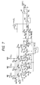
- Fig. 7 is a circuit constructional diagram showing the fourth embodiment of a peak detecting apparatus of the invention.
- the peak detecting apparatus shown in Fig. 4 when the terminal Phi-RES is first set to the L level, an output voltage rises and, after that, a signal component is further read out. Therefore, when a voltage difference between an output of a dummy cell and a signal output is large and a gain of a gain amplifier at the post stage is so high to be tens of times, there is a case where the amplifier is saturated. As shown in Fig.
- a reset voltage source and an output line of a dummy output unit are connected through two serial resistors and are connected to a buffer amplifier by dividing resistances, thereby raising an output of the dummy cell, reducing a differential voltage between them, and preventing a saturation of the amplifier.
- the terminal Phi-RES is set to the L level and an output voltage is increased by an emitter current of the transistors Q 31 to Q 33 .
- the reset voltage is resistance divided and an output voltage is formed and a differential signal between both of the output voltages is generated, the output voltage of the amount raised by the emitter current of the transistors Q 31 to Q 33 can be eliminated.
- Fig. 8 is a circuit constructional diagram showing the fifth embodiment of a peak detecting apparatus of the invention.
- a clamping circuit constructed by a capacitor C CL and an MOS transistor M CL is connected to the final output stage of the peak detecting apparatus of the fourth embodiment shown in Fig. 7 and a comparator C 1 is connected to an output of the clamping circuit.
- the same control signal as a control signal (reset signal) that is applied to the terminal Phi-CL is supplied to a terminal Phi-SH which is connected to a gate of the MOS transistor M CL .
- a control signal (reset signal) that is applied to the terminal Phi-CL is supplied to a terminal Phi-SH which is connected to a gate of the MOS transistor M CL .
- an electric potential on the output side of the capacitor C CL (connecting side to the comparator C 1 ) is set to V REF2 .
- a peak voltage of the signal from which the noise component is eliminated is clamped and inputted to the comparator C 1 .
- the comparator C 1 the clamped peak voltage and a reference voltage V X are compared.
- the peak detecting apparatus of the embodiment is preferably used in an application as a detector.
- the embodiment has been shown and described with respect to the case where the clamping circuit and comparator are connected to the final output stage of the peak detecting apparatus of the embodiment 4. However, it will be obviously understood that the clamping circuit and comparator can be also connected to the final output stage of the peak detecting apparatus in each of the embodiments 1 to 3.
- the sixth embodiment relates to the improvement of the peak detecting apparatus of the fifth embodiment.
- Fig. 9 is a timing chart of a peak detecting apparatus of the embodiment.
- the noise reading operation is executed twice.
- the first noise reading operation is executed to hold the noise signal into the capacitors CC 1 to CC 3 and capacitors CT 1 to CT 3 .
- the next noise reading operation is executed to decide a clamping voltage of the clamping circuit at the front stage of the comparator C 1 .
- a circuit construction of the peak detecting apparatus in the embodiment is similar to that of Fig. 8.
- a waveform at an output terminal OUT when the noise is read out and that when the sensor signal including the noise is read out are different.
- the noise is read out from V A to V B .
- the emitter voltage of the NPN transistors Q 31 to Q 33 at the front stage of the amplifier also has a shape similar to the foregoing waveform. Therefore, operating regions of the transistors are different in both cases. When the sensor signal is very small, it is also considered that a detection error based on it occurs.
- the noise reading operation is added and on the basis of an output voltage at this time, a comparing operation is executed at the final stage. Operating points of the reading circuit including Q 31 to Q 33 at the time of the second noise reading operation and at the time of the second reading operation of the sensor signal including the noise coincide and the accurate detection can be performed.
- the input sides of the capacitors CC 1 to CC 3 are set to the GND potential and the output sides of the capacitors CC to CC 3 and the capacitors CT 1 to CT 3 are set to a potential (V CL - V 1 ).
- the output potential of the amplifier A 1 also drops in correspondence to the potential fluctuation.
- the noise reading operation is again performed. Namely, when the terminal Phi-RES is set to the low level and the noise reading operation is again executed, the input sides of the capacitors CC 1 to CC 3 are set to the noise potential V 1 and the output sides of the capacitors CC 1 to CC 3 and the capacitors CT 1 to CT 3 are set to the potential V CL .
- the output potential of the amplifier A 1 also rises in correspondence to the potential fluctuation, in this instance, by setting the terminal Phi-SH to the L level, the electric potential on the output side of the capacitor C CL is set to V REF2 and the clamping voltage is specified.
- the input sides of the capacitors CC 1 to CC 3 are set to the GND potential and the output sides of the capacitors CC 1 to CC 3 and the capacitors CT 1 to CT 3 are set to the electric potential (V CL - V 1 ).
- the output potential of the amplifier A 1 also drops in correspondence to the potential fluctuation.
- the electric potential on the output side of the capacitor C CL is set to (V REF2 - V 1 ).
- the electric potential on the output side of the capacitor C CL is set to (V REF2 - V 1 + V 2 ). Namely, in the second noise reading operation and the second reading operation of the signal including the noise, since the electric potentials of the capacitors CT 1 to CT 3 can be set to the same value, even a micro signal can be also accurately detected.
- the peak detecting apparatuses of the invention when the peak value of the signals from the plurality of signal sources is detected, a peak detecting precision can be improved.
Landscapes
- Engineering & Computer Science (AREA)
- Power Engineering (AREA)
- Physics & Mathematics (AREA)
- General Physics & Mathematics (AREA)
- Measurement Of Current Or Voltage (AREA)
- Manipulation Of Pulses (AREA)
Applications Claiming Priority (2)
| Application Number | Priority Date | Filing Date | Title |
|---|---|---|---|
| JP8015676A JPH09211037A (ja) | 1996-01-31 | 1996-01-31 | ピーク検出装置 |
| JP15676/96 | 1996-01-31 |
Publications (3)
| Publication Number | Publication Date |
|---|---|
| EP0788229A2 true EP0788229A2 (de) | 1997-08-06 |
| EP0788229A3 EP0788229A3 (de) | 1998-07-29 |
| EP0788229B1 EP0788229B1 (de) | 2009-06-17 |
Family
ID=11895361
Family Applications (1)
| Application Number | Title | Priority Date | Filing Date |
|---|---|---|---|
| EP97300558A Expired - Lifetime EP0788229B1 (de) | 1996-01-31 | 1997-01-29 | Spitzenwertermittlungsgerät |
Country Status (4)
| Country | Link |
|---|---|
| US (1) | US5942920A (de) |
| EP (1) | EP0788229B1 (de) |
| JP (1) | JPH09211037A (de) |
| DE (1) | DE69739452D1 (de) |
Cited By (2)
| Publication number | Priority date | Publication date | Assignee | Title |
|---|---|---|---|---|
| RU2166835C1 (ru) * | 2000-03-31 | 2001-05-10 | Ульяновский государственный технический университет | Экстрематор напряжения |
| EP2063671A2 (de) | 2007-11-22 | 2009-05-27 | Yamaha Corporation | Verstärkersystem |
Families Citing this family (3)
| Publication number | Priority date | Publication date | Assignee | Title |
|---|---|---|---|---|
| US6781624B1 (en) * | 1998-07-30 | 2004-08-24 | Canon Kabushiki Kaisha | Signal processing apparatus |
| US6870358B2 (en) * | 2001-12-31 | 2005-03-22 | Baes Systems Information And Electronic Systems Integration Inc. | Methods and apparatuses for peak detection among multiple signals |
| CN109633245B (zh) * | 2019-01-15 | 2020-12-01 | 电子科技大学 | 一种新型峰值检测电路 |
Family Cites Families (5)
| Publication number | Priority date | Publication date | Assignee | Title |
|---|---|---|---|---|
| US3719895A (en) * | 1971-03-11 | 1973-03-06 | Northern Electric Co | Automatic gain control circuit |
| KR950013443B1 (ko) * | 1987-09-18 | 1995-11-08 | 상요 덴기 가부시기가이샤 | Ic화에 적합한 피이크 홀드 회로 |
| US4937670A (en) * | 1989-01-31 | 1990-06-26 | Rca Licensing Corporation | Peak detector with feedback |
| JP2958992B2 (ja) * | 1989-10-31 | 1999-10-06 | 日本電気株式会社 | 半導体集積回路 |
| US5302863A (en) * | 1993-01-29 | 1994-04-12 | Hewlett-Packard Company | CMOS peak amplitude detector |
-
1996
- 1996-01-31 JP JP8015676A patent/JPH09211037A/ja active Pending
-
1997
- 1997-01-28 US US08/789,871 patent/US5942920A/en not_active Expired - Fee Related
- 1997-01-29 DE DE69739452T patent/DE69739452D1/de not_active Expired - Lifetime
- 1997-01-29 EP EP97300558A patent/EP0788229B1/de not_active Expired - Lifetime
Cited By (4)
| Publication number | Priority date | Publication date | Assignee | Title |
|---|---|---|---|---|
| RU2166835C1 (ru) * | 2000-03-31 | 2001-05-10 | Ульяновский государственный технический университет | Экстрематор напряжения |
| EP2063671A2 (de) | 2007-11-22 | 2009-05-27 | Yamaha Corporation | Verstärkersystem |
| EP2063671A3 (de) * | 2007-11-22 | 2009-11-04 | Yamaha Corporation | Verstärkersystem |
| US8401680B2 (en) | 2007-11-22 | 2013-03-19 | Yamaha Corporation | Amplifier system |
Also Published As
| Publication number | Publication date |
|---|---|
| JPH09211037A (ja) | 1997-08-15 |
| DE69739452D1 (de) | 2009-07-30 |
| EP0788229A3 (de) | 1998-07-29 |
| US5942920A (en) | 1999-08-24 |
| EP0788229B1 (de) | 2009-06-17 |
Similar Documents
| Publication | Publication Date | Title |
|---|---|---|
| EP0520432B1 (de) | Signalverarbeitungsschaltung und System zur Erfassung eines Absolutbetrages | |
| US3985954A (en) | DC level control circuit | |
| JPH0420238B2 (de) | ||
| US20210287723A1 (en) | Self-biased sense amplification circuit | |
| US4801788A (en) | Bar code scanner for a video signal which has a shading waveform | |
| US4445054A (en) | Full-wave rectifying circuit | |
| US5942920A (en) | Dual buffer peak detecting apparatus | |
| EP0326695A2 (de) | BIMOS-Speicher-Abfühlverstärkersystem | |
| US3694748A (en) | Peak-to-peak detector | |
| US6628147B2 (en) | Comparator having reduced sensitivity to offset voltage and timing errors | |
| EP1056196A2 (de) | Verstärkerschaltung | |
| HK1001879A (en) | Peak detecting apparatus | |
| EP0478389A1 (de) | Verstärken mit polygonförmiger Ausgangscharakteristik | |
| US3309538A (en) | Sensitive sense amplifier circuits capable of discriminating marginal-level info-signals from noise yet unaffected by parameter and temperature variations | |
| JP2020177009A (ja) | 地絡検出装置 | |
| EP0785440A2 (de) | Signalerzeugungsschaltung und Spitzenwertdetektorschaltung | |
| JPH0918745A (ja) | 映像信号クランプ回路 | |
| US3461318A (en) | Monolithically fabricated sense amplifier-threshold detector | |
| JP3701037B2 (ja) | サンプル・ホールド回路 | |
| US5155395A (en) | Filter circuit comprising an amplifier and a capacitor | |
| US4647796A (en) | Multiple level voltage comparator circuit | |
| JPH0671315B2 (ja) | フイ−ドバツク型クランプ回路 | |
| CN110987197A (zh) | 信号处理装置及方法 | |
| JP3165173B2 (ja) | 静電容量センサ回路 | |
| JPS638673B2 (de) |
Legal Events
| Date | Code | Title | Description |
|---|---|---|---|
| PUAI | Public reference made under article 153(3) epc to a published international application that has entered the european phase |
Free format text: ORIGINAL CODE: 0009012 |
|
| AK | Designated contracting states |
Kind code of ref document: A2 Designated state(s): DE ES FR GB IT NL |
|
| PUAL | Search report despatched |
Free format text: ORIGINAL CODE: 0009013 |
|
| AK | Designated contracting states |
Kind code of ref document: A3 Designated state(s): DE ES FR GB IT NL |
|
| 17P | Request for examination filed |
Effective date: 19981210 |
|
| 17Q | First examination report despatched |
Effective date: 20020620 |
|
| GRAP | Despatch of communication of intention to grant a patent |
Free format text: ORIGINAL CODE: EPIDOSNIGR1 |
|
| GRAS | Grant fee paid |
Free format text: ORIGINAL CODE: EPIDOSNIGR3 |
|
| GRAA | (expected) grant |
Free format text: ORIGINAL CODE: 0009210 |
|
| AK | Designated contracting states |
Kind code of ref document: B1 Designated state(s): DE ES FR GB IT NL |
|
| REG | Reference to a national code |
Ref country code: GB Ref legal event code: FG4D |
|
| REF | Corresponds to: |
Ref document number: 69739452 Country of ref document: DE Date of ref document: 20090730 Kind code of ref document: P |
|
| NLV1 | Nl: lapsed or annulled due to failure to fulfill the requirements of art. 29p and 29m of the patents act | ||
| PG25 | Lapsed in a contracting state [announced via postgrant information from national office to epo] |
Ref country code: ES Free format text: LAPSE BECAUSE OF FAILURE TO SUBMIT A TRANSLATION OF THE DESCRIPTION OR TO PAY THE FEE WITHIN THE PRESCRIBED TIME-LIMIT Effective date: 20090928 |
|
| PG25 | Lapsed in a contracting state [announced via postgrant information from national office to epo] |
Ref country code: NL Free format text: LAPSE BECAUSE OF FAILURE TO SUBMIT A TRANSLATION OF THE DESCRIPTION OR TO PAY THE FEE WITHIN THE PRESCRIBED TIME-LIMIT Effective date: 20090617 |
|
| PLBE | No opposition filed within time limit |
Free format text: ORIGINAL CODE: 0009261 |
|
| STAA | Information on the status of an ep patent application or granted ep patent |
Free format text: STATUS: NO OPPOSITION FILED WITHIN TIME LIMIT |
|
| 26N | No opposition filed |
Effective date: 20100318 |
|
| REG | Reference to a national code |
Ref country code: HK Ref legal event code: WD Ref document number: 1001879 Country of ref document: HK |
|
| GBPC | Gb: european patent ceased through non-payment of renewal fee |
Effective date: 20100129 |
|
| REG | Reference to a national code |
Ref country code: FR Ref legal event code: ST Effective date: 20100930 |
|
| PG25 | Lapsed in a contracting state [announced via postgrant information from national office to epo] |
Ref country code: FR Free format text: LAPSE BECAUSE OF NON-PAYMENT OF DUE FEES Effective date: 20100201 |
|
| PG25 | Lapsed in a contracting state [announced via postgrant information from national office to epo] |
Ref country code: GB Free format text: LAPSE BECAUSE OF NON-PAYMENT OF DUE FEES Effective date: 20100129 |
|
| PG25 | Lapsed in a contracting state [announced via postgrant information from national office to epo] |
Ref country code: IT Free format text: LAPSE BECAUSE OF FAILURE TO SUBMIT A TRANSLATION OF THE DESCRIPTION OR TO PAY THE FEE WITHIN THE PRESCRIBED TIME-LIMIT Effective date: 20090617 |
|
| PGFP | Annual fee paid to national office [announced via postgrant information from national office to epo] |
Ref country code: DE Payment date: 20110131 Year of fee payment: 15 |
|
| PG25 | Lapsed in a contracting state [announced via postgrant information from national office to epo] |
Ref country code: DE Free format text: LAPSE BECAUSE OF NON-PAYMENT OF DUE FEES Effective date: 20120801 |
|
| REG | Reference to a national code |
Ref country code: DE Ref legal event code: R119 Ref document number: 69739452 Country of ref document: DE Effective date: 20120801 |