EP0789417A1 - Résonateur diélectrique - Google Patents
Résonateur diélectrique Download PDFInfo
- Publication number
- EP0789417A1 EP0789417A1 EP97101992A EP97101992A EP0789417A1 EP 0789417 A1 EP0789417 A1 EP 0789417A1 EP 97101992 A EP97101992 A EP 97101992A EP 97101992 A EP97101992 A EP 97101992A EP 0789417 A1 EP0789417 A1 EP 0789417A1
- Authority
- EP
- European Patent Office
- Prior art keywords
- dielectric resonator
- resonance frequency
- mode
- cavity
- hole
- Prior art date
- Legal status (The legal status is an assumption and is not a legal conclusion. Google has not performed a legal analysis and makes no representation as to the accuracy of the status listed.)
- Granted
Links
- 239000004020 conductor Substances 0.000 claims abstract description 33
- 238000000034 method Methods 0.000 claims description 19
- 230000007423 decrease Effects 0.000 claims description 10
- 230000009977 dual effect Effects 0.000 claims description 9
- 239000000919 ceramic Substances 0.000 description 4
- 229910052751 metal Inorganic materials 0.000 description 3
- 239000002184 metal Substances 0.000 description 3
- BQCADISMDOOEFD-UHFFFAOYSA-N Silver Chemical compound [Ag] BQCADISMDOOEFD-UHFFFAOYSA-N 0.000 description 2
- 239000000853 adhesive Substances 0.000 description 2
- 230000001070 adhesive effect Effects 0.000 description 2
- 229910052709 silver Inorganic materials 0.000 description 2
- 239000004332 silver Substances 0.000 description 2
- 238000004891 communication Methods 0.000 description 1
- 239000003989 dielectric material Substances 0.000 description 1
- 230000001747 exhibiting effect Effects 0.000 description 1
- 230000010354 integration Effects 0.000 description 1
- 238000012986 modification Methods 0.000 description 1
- 230000004048 modification Effects 0.000 description 1
- 238000000465 moulding Methods 0.000 description 1
Images




Classifications
-
- H—ELECTRICITY
- H01—ELECTRIC ELEMENTS
- H01P—WAVEGUIDES; RESONATORS, LINES, OR OTHER DEVICES OF THE WAVEGUIDE TYPE
- H01P7/00—Resonators of the waveguide type
- H01P7/10—Dielectric resonators
Definitions
- the present invention relates to a dielectric resonator comprising of a TM dual-mode dielectric resonator element disposed in a cavity.
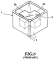
- Fig. 6 illustrates the structure of a conventional TM dual-mode dielectric resonator.
- areas filled with dots represent those portions on which a conductor is formed.
- the dielectric resonator shown in Fig. 6 comprises a TM dual-mode dielectric resonator element 2 disposed in an integral fashion in a cavity 1 serving as a waveguide.
- the dielectric resonator element 2 is made up of dielectric ceramic in such a manner that two rectangular resonator elements 2a and 2b each exhibiting resonance in a TM mode are integrated into one piece in a cross shape whereby the two resonator elements 2a and 2b are perpendicular to each other.
- the cavity 1 is formed with a rectangular-shaped frame of dielectric ceramic produced in an integral fashion together with the dielectric resonator element 2 by molding wherein each open side of the frame is closed with a side plate (not shown).
- the whole outer surface of cavity 1 is coated with a cavity conductor 3 such as Ag.
- Each side plate is made up of a dielectric ceramic plate whose surface is covered with a conductor or made up of a conductive metal plate. Alternatively, each side plate may also be realized by means of utilizing a part of a metal case in which the dielectric resonator is disposed.
- TM 110 dual mode dielectric resonator acts as a two-stage dielectric resonator composed of two resonator elements.
- This type of dielectric resonator is used, for example, as a dielectric filter in a communication device.
- a dielectric resonator including two dielectric resonator elements perpendicular to each other and disposed in an integral fashion in a cavity so as to form a TM dual-mode dielectric resonator element, the dielectric resonator having a hole formed in the TM dual-mode dielectric resonator element, that the hole extending from the outer surface of the cavity wall toward the inner portion of the TM dual-mode dielectric resonator element along its axis, the inner wall of the hole being covered with a conductor electrically connected to a cavity conductor, the hole being formed so that the TM 110-mode resonance frequency of the TM dual-mode dielectric resonator element is substantially equal to the TM 111-mode resonance frequency.
- a dielectric resonator including two dielectric resonator elements perpendicular to each other and disposed in an integral fashion in a cavity so as to form a TM dual-mode dielectric resonator element, the dielectric resonator having a hole formed in the intersection of the two dielectric resonator elements of the TM dual-mode dielectric resonator element, the hole being formed so that the TM 110-mode resonance frequency of the TM dual-mode dielectric resonator element is substantially equal to the TM 111-mode resonance frequency.
- a dielectric resonator including two dielectric resonator elements perpendicular to each other and disposed in an integral fashion in a cavity so as to form a TM dual-mode dielectric resonator element, the dielectric resonator having a first hole formed in the TM dual-mode dielectric resonator element the first hole extending from the outer surface of the cavity wall toward the inner portion of the TM dual-mode dielectric resonator element along its axis, the inner wall of the first hole being covered with a conductor electrically connected to a cavity conductor; and a second hole being formed in the intersection of the two dielectric resonator elements of the TM dual-mode dielectric resonator element, the first and second holes being formed so that the TM 110-mode resonance frequency of the TM dual-mode dielectric resonator element is substantially equal to the TM 111-mode resonance frequency.
- the hole(s) is (are) formed in a proper form and at a proper location in the TM dual-mode dielectric resonator element so that the TM dual-mode dielectric resonator has the same resonance frequency for both TM 110 and TM 111 modes thereby achieving high performance similar to that of a conventional TM three-mode dielectric resonator without having to increase the overall size.
- the capacitance of the TM dual-mode resonator element changes and thus the resonance frequency associated with each TM mode also changes.
- the change in resonance frequency associated with TM 110 mode occurs at a different fashion from that of TM 111 mode, and it is possible to obtain the same resonance frequency for both TM 110 and TM 111 modes by properly selecting the shape and/or the location of the hole.
- Fig. 1 illustrates the structure of a first embodiment of a dielectric resonator according to the present invention wherein Fig. 1(a) is a perspective view illustrating the external appearance and Fig. 1(b) is a side view of the dielectric resonator shown in Fig. 1(a).
- the dielectric resonator of this embodiment includes a cross-shaped TM dual-mode dielectric resonator element 2 disposed in an integral form in a cavity 1.
- the TM dual-mode dielectric resonator element 2 is composed of resonator elements 2a and 2b both ends of each of which are connected to the wall of the cavity 1.
- a hole 4a with a closed end is formed in a central part of each connecting portion between each resonator element 2a, 2b and the cavity wall in such a manner that each hole 4a extends from the outer surface of the cavity wall toward the inner portion of each resonator element 2a, 2b.
- each hole 4a is covered with a conductor 3a which is electrically connected to the cavity conductor 3.
- holes 4a are formed along the axes of the respective resonator elements 2a and 2b and the cavity conductor 3 also extends over the inner surface of each hole 4a.
- the conductor 3a is thus a part of the cavity conductor 3.
- each hole 4a The geometric structure, that is, the diameter and the depth of each hole 4a are selected so that the TM dual-mode dielectric resonator element 2 has the same resonance frequency for both TM 110 and TM 111 modes.
- the other parts except for the holes 4a are constructed in the same manner as in the conventional resonator shown in Fig. 6 and thus they are not described in further detail here.
- Fig. 2 illustrates the changes in resonance frequencies in TM 110 and TM 111 modes as a function of the depth of the hole 4a formed in accordance with the present embodiment.
- the resonance frequency decreases in both TM 110 and TM 111-modes as shown in Fig. 2.
- the TM 111-mode has a higher resonance frequency than the TM 110-mode in a shallow depth range, the TM 111-mode resonance frequency decreases at a greater rate with the increase in the depth of the hole 4a than the TM 110-mode resonance frequency. Therefore, the TM 111-mode resonance frequency becomes the same as the TM 110-mode resonance frequency at a certain depth.
- TM 110-mode and TM 111-mode resonance frequencies it is possible to set the TM 110-mode and TM 111-mode resonance frequencies so that they have the same value by properly selecting the diameters and the depths of the holes 4a.
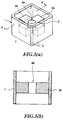
- Fig. 3 illustrates the structure of a second embodiment of a dielectric resonator according to the present invention wherein Fig. 3(a) is a perspective view illustrating its external appearance and Fig. 3(b) is a cross-sectional view of the dielectric resonator shown in Fig. 3(a) taken along line X-X.
- a hole 4b having a circular shape in cross section is formed in a central portion of a dielectric resonator element 2 at which two resonator elements 2a and 2b cross each other.
- the hole 4b extends through the dielectric resonator element 2 in a direction (in a vertical direction in Fig. 2) across its thickness from one side to the opposite side.
- the diameter of the hole 4b is selected so that the TM dual-mode dielectric resonator element 2 has the same resonance frequency for both TM 110 and TM 111-modes.
- the other parts except the hole 4b are constructed in the same manner as in the conventional dielectric resonator shown in Fig. 6 and they are not described in further detail here.
- Fig. 4 illustrates the changes in resonance frequencies in TM 110 and TM 111-modes as a function of the diameter of the hole 4b formed in accordance with the present embodiment.
- the capacitance of the dielectric resonator element 2 decreases with the increase in the diameter of the hole 4b.
- both the TM 110-mode and TM 111-mode resonance frequencies increase as shown in Fig. 4.
- the TM 110-mode has a lower resonance frequency than the TM 111-mode in a small-diameter range
- the TM 110-mode resonance frequency increases at a greater rate with the increase in the diameter of the hole 4b than the TM 111-mode resonance frequency. Therefore, the TM 110-mode resonance frequency is the same as the TM 111-mode resonance frequency at a certain diameter.
- the hole is formed through the dielectric resonator element such that it extends from one side to the opposite side of the resonator element, the hole may also be formed in such a manner that it has a closed end.
- Fig. 5 is a perspective view illustrating the structure of a third embodiment of a dielectric resonator according to the present invention.
- a hole 4b having a circular shape in cross section is formed in the intersection of two resonator elements 2a and 2b wherein the hole 4b extends through the dielectric resonator element 2 in a direction across its thickness.
- a hole 4a for example, quadrangular pyramid-shaped hole 4a having a closed end, is formed in each connecting part between each resonator element 2a, 2b and a cavity wall 1 in such a manner that each hole 4a extends from the outer surface of the cavity wall toward the inner portion of each resonator element 2a, 2b.
- the inner wall of each hole 4a is covered with a conductor 3a which is electrically connected to the cavity conductor 3.
- the shape of the holes 4a and 4b are determined so that the TM dual-mode dielectric resonator element 2 has the same resonance frequency for both TM 110 and TM 111-modes.
- the other parts except for the holes 4a and 4b are constructed in the same manner as in the conventional resonator shown in Fig. 6 and thus they are not described in further detail here.
- the dielectric resonator of the embodiment of Fig. 5, as described above, has a structure obtained by combining the structures of the first and second embodiments. This structure allows the capacitance of the dielectric resonator element 2 to be set in a more flexible manner than in the previous embodiments.
- TM 110-mode and TM 111-mode resonance frequencies it is possible to set the TM 110-mode and TM 111-mode resonance frequencies so that they have the same value by properly selecting the inner diameters, the locations, and the depths of the holes 4a formed along the axes of the dielectric resonator element 2 and of the hole 4b formed across its thickness.
- the holes 4a and 4b may be formed simultaneously in the process in which the dielectric resonator is formed, or may be formed by cutting or the like after forming the dielectric resonator.
- the dielectric resonator element 2 is formed in an integral fashion in the cavity, the dielectric resonator element and the cavity may also be formed separately and then combined into a single piece with a silver-filled adhesive or the like.
- the cavity itself may also be formed by combining six separately-formed ceramic plates coated with a conductor into a single piece with a silver-filled adhesive or the like.
- a metal case may also be employed to form the cavity.
- the hole(s) is (are) formed in a proper shape and at a proper location in the TM dual-mode resonator element so that the TM 110-mode resonance frequency of the TM dual-mode resonator element is equal to the TM 111-mode resonance frequency. This makes it possible to easily achieve high performance similar to that of a conventional TM three-mode dielectric resonator.
- Fig. 7 illustrates the structure of a dielectric resonator which is a variation of the third embodiment of the invention.
- a part of the dielectric resonator is cut away so as to show the internal structure of a hole.
- an elliptic cone-shaped hole 4a is formed in each connecting part between each end of two resonator elements 2a and 2b and a cavity wall 1 in such a manner that each hole 4a extends from the outer surface of the cavity wall 1 toward the inner portion of each resonator element 2a, 2b.
- the inner wall of each hole 4a is covered with a conductor 3a electrically connected to a cavity conductor 3.
- each hole 4a is determined so that the TM 110-mode resonance frequency of the TM dual-mode dielectric resonator element 2 is equal to the TM 111-mode resonance frequency.
- the other parts except for the holes 4a are constructed in the same manner as in the conventional resonator shown in Fig. 6 and thus they are not described in further detail here.
- the dielectric resonator of the present embodiment is different from the third embodiment described above in that the holes 4a are formed in a different shape.
- TM 110-mode and TM 111-mode resonance frequencies it is possible to set the TM 110-mode and TM 111-mode resonance frequencies so that they have the same value by properly selecting the inner diameters, the locations, and the depths of the holes 4a formed from the cavity wall into the dielectric resonator element 2 in directions perpendicular to the corresponding cavity wall, and also by properly selecting the size of the rectangular-shaped resonator and the relative dielectric constant ⁇ r of the dielectric material.
Landscapes
- Control Of Motors That Do Not Use Commutators (AREA)
Applications Claiming Priority (3)
| Application Number | Priority Date | Filing Date | Title |
|---|---|---|---|
| JP8021394A JP2998627B2 (ja) | 1996-02-07 | 1996-02-07 | 誘電体共振器 |
| JP21394/96 | 1996-02-07 | ||
| JP2139496 | 1996-02-07 |
Publications (2)
| Publication Number | Publication Date |
|---|---|
| EP0789417A1 true EP0789417A1 (fr) | 1997-08-13 |
| EP0789417B1 EP0789417B1 (fr) | 2002-04-03 |
Family
ID=12053855
Family Applications (1)
| Application Number | Title | Priority Date | Filing Date |
|---|---|---|---|
| EP97101992A Expired - Lifetime EP0789417B1 (fr) | 1996-02-07 | 1997-02-07 | Résonateur diélectrique |
Country Status (4)
| Country | Link |
|---|---|
| US (1) | US5796320A (fr) |
| EP (1) | EP0789417B1 (fr) |
| JP (1) | JP2998627B2 (fr) |
| DE (1) | DE69711476T2 (fr) |
Cited By (4)
| Publication number | Priority date | Publication date | Assignee | Title |
|---|---|---|---|---|
| EP0917238A1 (fr) * | 1997-11-05 | 1999-05-19 | Murata Manufacturing Co., Ltd. | Résonateur diélectrique, filtre diélectrique utilisant le résonateur diélectrique et duplexeur diélectrique |
| EP1056151A1 (fr) * | 1999-05-25 | 2000-11-29 | Murata Manufacturing Co., Ltd. | Résonateur diélectrique, filtre, duplexeur, oscillateur et dispositif de communication |
| CN106688138A (zh) * | 2015-06-30 | 2017-05-17 | 华为技术有限公司 | 三模介质谐振器和滤波器 |
| WO2020062686A1 (fr) * | 2018-09-30 | 2020-04-02 | 香港凡谷发展有限公司 | Structure de résonance à trois modes à cavité concave et filtre contenant une structure de résonance |
Families Citing this family (13)
| Publication number | Priority date | Publication date | Assignee | Title |
|---|---|---|---|---|
| JP3298485B2 (ja) * | 1997-02-03 | 2002-07-02 | 株式会社村田製作所 | 多重モード誘電体共振器 |
| JP3389868B2 (ja) * | 1998-11-09 | 2003-03-24 | 株式会社村田製作所 | 誘電体フィルタの自動特性調整方法、自動特性調整装置およびそれを用いた誘電体フィルタの製造方法 |
| US6650208B2 (en) * | 2001-06-07 | 2003-11-18 | Remec Oy | Dual-mode resonator |
| US7068127B2 (en) | 2001-11-14 | 2006-06-27 | Radio Frequency Systems | Tunable triple-mode mono-block filter assembly |
| US6853271B2 (en) | 2001-11-14 | 2005-02-08 | Radio Frequency Systems, Inc. | Triple-mode mono-block filter assembly |
| US7283022B2 (en) * | 2005-02-09 | 2007-10-16 | Powerwave Technologies, Inc. | Dual mode ceramic filter |
| KR101357027B1 (ko) | 2013-01-10 | 2014-02-04 | 세원텔레텍 주식회사 | 리엔트런트 캐비티형 유전체 공진기를 이용한 듀얼 모드 유전체 공진기 필터 |
| WO2016063997A1 (fr) * | 2014-10-21 | 2016-04-28 | 주식회사 케이엠더블유 | Resonateur multimode |
| WO2017088195A1 (fr) | 2015-11-28 | 2017-06-01 | 华为技术有限公司 | Résonateur diélectrique et filtre |
| EP4348760A4 (fr) * | 2021-07-09 | 2025-05-07 | Telefonaktiebolaget LM Ericsson (publ) | Résonateur à cavité diélectrique et filtre à cavité diélectrique le comprenant |
| EP4445445A4 (fr) * | 2022-03-23 | 2025-10-15 | Ericsson Telefon Ab L M | Résonateur diélectrique bimode tm et filtre bimode tm |
| WO2024025187A1 (fr) * | 2022-07-25 | 2024-02-01 | 주식회사 에이스테크놀로지 | Filtre à cavité ayant une structure miniaturisée |
| CN120113103A (zh) * | 2022-10-25 | 2025-06-06 | 上海诺基亚贝尔股份有限公司 | 谐振器和滤波器 |
Citations (4)
| Publication number | Priority date | Publication date | Assignee | Title |
|---|---|---|---|---|
| US4642591A (en) * | 1984-11-16 | 1987-02-10 | Murata Manufacturing Co., Ltd. | TM-mode dielectric resonance apparatus |
| JPH04296104A (ja) * | 1991-03-25 | 1992-10-20 | Murata Mfg Co Ltd | 多重モード誘電体共振器 |
| JPH08288717A (ja) * | 1995-04-18 | 1996-11-01 | Murata Mfg Co Ltd | 誘電体共振器 |
| EP0760534A2 (fr) * | 1995-09-01 | 1997-03-05 | Murata Manufacturing Co., Ltd. | Filtre diélectrique |
Family Cites Families (4)
| Publication number | Priority date | Publication date | Assignee | Title |
|---|---|---|---|---|
| JPH0828612B2 (ja) * | 1990-04-09 | 1996-03-21 | 株式会社村田製作所 | Tmモード誘電体共振器 |
| DE69428509T2 (de) * | 1993-12-28 | 2002-05-16 | Murata Mfg. Co., Ltd. | TM-Zweifachmodusresonator und -filter |
| JPH07245509A (ja) * | 1994-03-03 | 1995-09-19 | Murata Mfg Co Ltd | 非結合型誘電体共振器 |
| JP3339194B2 (ja) * | 1994-09-13 | 2002-10-28 | 株式会社村田製作所 | Tmモード誘電体共振器 |
-
1996
- 1996-02-07 JP JP8021394A patent/JP2998627B2/ja not_active Expired - Lifetime
-
1997
- 1997-02-06 US US08/796,254 patent/US5796320A/en not_active Expired - Lifetime
- 1997-02-07 DE DE69711476T patent/DE69711476T2/de not_active Expired - Lifetime
- 1997-02-07 EP EP97101992A patent/EP0789417B1/fr not_active Expired - Lifetime
Patent Citations (4)
| Publication number | Priority date | Publication date | Assignee | Title |
|---|---|---|---|---|
| US4642591A (en) * | 1984-11-16 | 1987-02-10 | Murata Manufacturing Co., Ltd. | TM-mode dielectric resonance apparatus |
| JPH04296104A (ja) * | 1991-03-25 | 1992-10-20 | Murata Mfg Co Ltd | 多重モード誘電体共振器 |
| JPH08288717A (ja) * | 1995-04-18 | 1996-11-01 | Murata Mfg Co Ltd | 誘電体共振器 |
| EP0760534A2 (fr) * | 1995-09-01 | 1997-03-05 | Murata Manufacturing Co., Ltd. | Filtre diélectrique |
Non-Patent Citations (2)
| Title |
|---|
| PATENT ABSTRACTS OF JAPAN vol. 17, no. 115 (E - 1330) 10 March 1993 (1993-03-10) * |
| YOUHEI ISHIKAWA ET AL: "800MHZ HIGH POWER DUPLEXER USING TM DUAL MODE DIELECTRIC RESONATORS", INTERNATIONAL MICROWAVE SYMPOSIUM DIGEST (MTT-S), ALBUQUERQUE, JUNE 1 - 5, 1992, vol. 3, 1 June 1992 (1992-06-01), REID D W, pages 1617 - 1620, XP000344478 * |
Cited By (8)
| Publication number | Priority date | Publication date | Assignee | Title |
|---|---|---|---|---|
| EP0917238A1 (fr) * | 1997-11-05 | 1999-05-19 | Murata Manufacturing Co., Ltd. | Résonateur diélectrique, filtre diélectrique utilisant le résonateur diélectrique et duplexeur diélectrique |
| US6064284A (en) * | 1997-11-05 | 2000-05-16 | Murata Manufacturing Co., Ltd. | Dielectric Resonator Device With A Thermal - Conducting Member |
| EP1056151A1 (fr) * | 1999-05-25 | 2000-11-29 | Murata Manufacturing Co., Ltd. | Résonateur diélectrique, filtre, duplexeur, oscillateur et dispositif de communication |
| US6429756B1 (en) | 1999-05-25 | 2002-08-06 | Murata Manufacturing Co., Ltd. | Dielectric resonator, filter, duplexer, oscillator and communication apparatus |
| CN106688138A (zh) * | 2015-06-30 | 2017-05-17 | 华为技术有限公司 | 三模介质谐振器和滤波器 |
| CN106688138B (zh) * | 2015-06-30 | 2019-06-14 | 华为技术有限公司 | 三模介质谐振器和滤波器 |
| WO2020062686A1 (fr) * | 2018-09-30 | 2020-04-02 | 香港凡谷发展有限公司 | Structure de résonance à trois modes à cavité concave et filtre contenant une structure de résonance |
| US11688920B2 (en) | 2018-09-30 | 2023-06-27 | Hongkong Fingu Development Company Limited | Concave triple-mode cavity resonance structure and filter with the resonance structure |
Also Published As
| Publication number | Publication date |
|---|---|
| JPH09214206A (ja) | 1997-08-15 |
| DE69711476D1 (de) | 2002-05-08 |
| JP2998627B2 (ja) | 2000-01-11 |
| DE69711476T2 (de) | 2002-07-18 |
| EP0789417B1 (fr) | 2002-04-03 |
| US5796320A (en) | 1998-08-18 |
Similar Documents
| Publication | Publication Date | Title |
|---|---|---|
| US5796320A (en) | Dielectric resonator | |
| US10090572B1 (en) | Radio frequency filter having a hollow box with a resonance element disposed therein and a depression with dot peen structures therein | |
| JP3298485B2 (ja) | 多重モード誘電体共振器 | |
| JP3389819B2 (ja) | 誘電体導波管型共振器 | |
| US5537082A (en) | Dielectric resonator apparatus including means for adjusting the degree of coupling | |
| EP0434296B1 (fr) | Résonateur diélectrique, dispositif à filtrage l'utilisant et procédé de production d'un tel résonateur diélectrique | |
| US5712648A (en) | Dielectric filter and antenna duplexer | |
| JPH05335808A (ja) | 誘電体共振器 | |
| JPH01112801A (ja) | 誘電体帯域フィルタ | |
| EP0731522B1 (fr) | Filtre diélectrique | |
| JP3620525B2 (ja) | 誘電体導波管型フィルタ及びその特性調整方法 | |
| CN114335968A (zh) | 一种双模介质谐振器及滤波器 | |
| JPH07235804A (ja) | 誘電体フィルタ | |
| JPH11127002A (ja) | 誘電体フィルタ | |
| JP3738916B2 (ja) | 誘電体共振器 | |
| CN218770035U (zh) | 一种金属谐振器 | |
| JPH10308604A (ja) | 誘電体フィルタ、誘電体デュプレクサおよびそれらの設計方法 | |
| JP3412546B2 (ja) | 誘電体フィルタ、誘電体デュプレクサ及び通信機装置 | |
| US5994981A (en) | Dielectric filter having obliquely oriented stepped resonators | |
| JP3125671B2 (ja) | 誘電体フィルタ | |
| KR102448010B1 (ko) | 웨이브가이드 필터 | |
| JP2000323909A (ja) | 誘電体共振器の製造方法、誘電体フィルタの製造方法、デュプレクサの製造方法、通信機装置の製造方法 | |
| JP3159025B2 (ja) | 誘電体フィルタ | |
| JP2555204Y2 (ja) | 誘電体共振器 | |
| JPH03149903A (ja) | 誘電体共振器装置および誘電体フィルタ |
Legal Events
| Date | Code | Title | Description |
|---|---|---|---|
| PUAI | Public reference made under article 153(3) epc to a published international application that has entered the european phase |
Free format text: ORIGINAL CODE: 0009012 |
|
| 17P | Request for examination filed |
Effective date: 19970207 |
|
| AK | Designated contracting states |
Kind code of ref document: A1 Designated state(s): DE GB IT SE |
|
| 17Q | First examination report despatched |
Effective date: 20000221 |
|
| GRAG | Despatch of communication of intention to grant |
Free format text: ORIGINAL CODE: EPIDOS AGRA |
|
| GRAG | Despatch of communication of intention to grant |
Free format text: ORIGINAL CODE: EPIDOS AGRA |
|
| GRAG | Despatch of communication of intention to grant |
Free format text: ORIGINAL CODE: EPIDOS AGRA |
|
| GRAH | Despatch of communication of intention to grant a patent |
Free format text: ORIGINAL CODE: EPIDOS IGRA |
|
| GRAH | Despatch of communication of intention to grant a patent |
Free format text: ORIGINAL CODE: EPIDOS IGRA |
|
| REG | Reference to a national code |
Ref country code: GB Ref legal event code: IF02 |
|
| GRAA | (expected) grant |
Free format text: ORIGINAL CODE: 0009210 |
|
| AK | Designated contracting states |
Kind code of ref document: B1 Designated state(s): DE GB IT SE |
|
| REF | Corresponds to: |
Ref document number: 69711476 Country of ref document: DE Date of ref document: 20020508 |
|
| PLBE | No opposition filed within time limit |
Free format text: ORIGINAL CODE: 0009261 |
|
| STAA | Information on the status of an ep patent application or granted ep patent |
Free format text: STATUS: NO OPPOSITION FILED WITHIN TIME LIMIT |
|
| 26N | No opposition filed |
Effective date: 20030106 |
|
| PGFP | Annual fee paid to national office [announced via postgrant information from national office to epo] |
Ref country code: DE Payment date: 20160218 Year of fee payment: 20 Ref country code: IT Payment date: 20160223 Year of fee payment: 20 |
|
| PGFP | Annual fee paid to national office [announced via postgrant information from national office to epo] |
Ref country code: SE Payment date: 20160217 Year of fee payment: 20 Ref country code: GB Payment date: 20160217 Year of fee payment: 20 |
|
| REG | Reference to a national code |
Ref country code: DE Ref legal event code: R071 Ref document number: 69711476 Country of ref document: DE |
|
| REG | Reference to a national code |
Ref country code: GB Ref legal event code: PE20 Expiry date: 20170206 |
|
| REG | Reference to a national code |
Ref country code: SE Ref legal event code: EUG |
|
| PG25 | Lapsed in a contracting state [announced via postgrant information from national office to epo] |
Ref country code: GB Free format text: LAPSE BECAUSE OF EXPIRATION OF PROTECTION Effective date: 20170206 |