EP0789445A1 - Convertisseur de courant electrique - Google Patents
Convertisseur de courant electrique Download PDFInfo
- Publication number
- EP0789445A1 EP0789445A1 EP96927196A EP96927196A EP0789445A1 EP 0789445 A1 EP0789445 A1 EP 0789445A1 EP 96927196 A EP96927196 A EP 96927196A EP 96927196 A EP96927196 A EP 96927196A EP 0789445 A1 EP0789445 A1 EP 0789445A1
- Authority
- EP
- European Patent Office
- Prior art keywords
- thyristor
- thyristor valve
- supplied
- power
- gate power
- Prior art date
- Legal status (The legal status is an assumption and is not a legal conclusion. Google has not performed a legal analysis and makes no representation as to the accuracy of the status listed.)
- Granted
Links
Images


Classifications
-
- H—ELECTRICITY
- H02—GENERATION; CONVERSION OR DISTRIBUTION OF ELECTRIC POWER
- H02M—APPARATUS FOR CONVERSION BETWEEN AC AND AC, BETWEEN AC AND DC, OR BETWEEN DC AND DC, AND FOR USE WITH MAINS OR SIMILAR POWER SUPPLY SYSTEMS; CONVERSION OF DC OR AC INPUT POWER INTO SURGE OUTPUT POWER; CONTROL OR REGULATION THEREOF
- H02M1/00—Details of apparatus for conversion
- H02M1/08—Circuits specially adapted for the generation of control voltages for semiconductor devices incorporated in static converters
- H02M1/088—Circuits specially adapted for the generation of control voltages for semiconductor devices incorporated in static converters for the simultaneous control of series or parallel connected semiconductor devices
- H02M1/092—Circuits specially adapted for the generation of control voltages for semiconductor devices incorporated in static converters for the simultaneous control of series or parallel connected semiconductor devices the control signals being transmitted optically
-
- H—ELECTRICITY
- H02—GENERATION; CONVERSION OR DISTRIBUTION OF ELECTRIC POWER
- H02M—APPARATUS FOR CONVERSION BETWEEN AC AND AC, BETWEEN AC AND DC, OR BETWEEN DC AND DC, AND FOR USE WITH MAINS OR SIMILAR POWER SUPPLY SYSTEMS; CONVERSION OF DC OR AC INPUT POWER INTO SURGE OUTPUT POWER; CONTROL OR REGULATION THEREOF
- H02M1/00—Details of apparatus for conversion
- H02M1/08—Circuits specially adapted for the generation of control voltages for semiconductor devices incorporated in static converters
-
- H—ELECTRICITY
- H03—ELECTRONIC CIRCUITRY
- H03K—PULSE TECHNIQUE
- H03K17/00—Electronic switching or gating, i.e. not by contact-making and –breaking
- H03K17/08—Modifications for protecting switching circuit against overcurrent or overvoltage
- H03K17/081—Modifications for protecting switching circuit against overcurrent or overvoltage without feedback from the output circuit to the control circuit
- H03K17/0814—Modifications for protecting switching circuit against overcurrent or overvoltage without feedback from the output circuit to the control circuit by measures taken in the output circuit
- H03K17/08144—Modifications for protecting switching circuit against overcurrent or overvoltage without feedback from the output circuit to the control circuit by measures taken in the output circuit in thyristor switches
-
- H—ELECTRICITY
- H03—ELECTRONIC CIRCUITRY
- H03K—PULSE TECHNIQUE
- H03K17/00—Electronic switching or gating, i.e. not by contact-making and –breaking
- H03K17/08—Modifications for protecting switching circuit against overcurrent or overvoltage
- H03K17/082—Modifications for protecting switching circuit against overcurrent or overvoltage by feedback from the output to the control circuit
- H03K17/0824—Modifications for protecting switching circuit against overcurrent or overvoltage by feedback from the output to the control circuit in thyristor switches
-
- H—ELECTRICITY
- H03—ELECTRONIC CIRCUITRY
- H03K—PULSE TECHNIQUE
- H03K17/00—Electronic switching or gating, i.e. not by contact-making and –breaking
- H03K17/10—Modifications for increasing the maximum permissible switched voltage
- H03K17/105—Modifications for increasing the maximum permissible switched voltage in thyristor switches
-
- H—ELECTRICITY
- H03—ELECTRONIC CIRCUITRY
- H03K—PULSE TECHNIQUE
- H03K17/00—Electronic switching or gating, i.e. not by contact-making and –breaking
- H03K17/51—Electronic switching or gating, i.e. not by contact-making and –breaking characterised by the components used
- H03K17/78—Electronic switching or gating, i.e. not by contact-making and –breaking characterised by the components used using opto-electronic devices, i.e. light-emitting and photoelectric devices electrically- or optically-coupled
- H03K17/79—Electronic switching or gating, i.e. not by contact-making and –breaking characterised by the components used using opto-electronic devices, i.e. light-emitting and photoelectric devices electrically- or optically-coupled controlling bipolar semiconductor switches with more than two PN-junctions, or more than three electrodes, or more than one electrode connected to the same conductivity region
Definitions
- This invention relates to a power converter for converting an alternating current to a direct current, or vice versa.
- FIG. 2 shows a conventional power converter comprising a thyristor valve and a controller for controlling the thyristor valve.
- the thyristor valve has a plurality of light-triggered thyristor (hereinafter referred to as "thyristor") LLT which is connected in series.
- the thyristor is used as a switching element, which allows an electric current to flow in only one direction.
- one voltage divider is connected in parallel to each thyristor.
- the voltage divider is a serial circuit being consisted of a capacitor C and a resistor R. Two reactors L are connected to the ends of the serial circuit of the thyristor LTT.
- the Reactors L also alleviate the rising curve of a surge voltage VS applied from the outside to the thyristors LTTs when the surge voltage VS is applied to the thyristor LTT.
- Each thyristor LTT is connected in parallel with light emitting diodes LEDF and LEDR.
- the diode LEDF emits light when a forward bias voltage is applied to the thyristor LTT, and the diode LEDR emits light when a reverse voltage is applied to the thyristor LTT.
- the currents flowing into the light-emitting diodes LEDF and LEDR are controlled by a resistor RD.
- the light beams emitted from the LEDF and LEDR are transmitted through light guides LGs to a pulse generator PG which is set at a ground potential.
- the pulse generator PG comprises a light-electric converter LEC for converting the light signals transmitted from the light emitting diodes LEDF and LEDR into a forward voltage signal FV and a backward voltage signal RV.
- the forward voltage signal FV and reverse voltage signal RV are used to determine a timing when the pulse generator generates a pulse to control the gate of the thyristor LTT.
- the pulse generator PG includes serially connected light emitting diodes LEDs in the same number as the thyristors LTTs.
- the serial circuit of the light emitting diodes LEDs is connected to a power source E through a switching element S1 and an impedance Z1 in series.
- LG1 is a logic circuit for controlling the switching device S1
- AMP1 is an amplifier for outputting an ON/OFF signal for turning on and off the switching device S1, upon receipt of the output of the logic circuit LG1.
- the thyristor valve has an arrester Ar.
- the arrester Ar controls the level of a surge voltage VS applied externally to coordinate with the withstand voltage of the thyristor LTT (abbreviated VDRM).
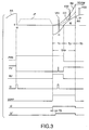
- FIG. 3 shows a timing chart representing the relationship between the waveforms of voltage and currents and the gate pulse.
- FIG. 3 is prepared for explain the feature of the present invention, but is used here for explain the conventional art.
- the timing chart shows the waveforms comprising the thyristor valves of FIG. 2 which are bridged in a three-phase system and operated as an inverter.
- AA describes the voltage between the terminals of the thyristors LTTs
- IT describes a thyristor valve current
- BB describes a transient withstand voltage during the period between the time that the thyristor valve current IT is cut off and the time that the forward withstand voltage BB reaches the rated value VDRM.
- the thyristors LTTs are turned off in a reverse voltage period T1 between the time that the thyristor valve current IT is cut off and the time that the voltage AA recovers to the forward voltage.
- the reverse voltage period T1 is set at a value equal to the sum of the turning-off time of the thyristors LTTs and some extra time.
- a predetermined period TFP is required.
- the transient withstand voltage BB of the thyristors remains lower than AA, AA > BB, and no problem will occur.
- the thyristors LTTs cannot withstand the over-voltage, and may be broken down.
- PHS describes a gate pulse instruction signal input from a controller (not shown) to the logic circuit LG1 of the pulse generator PG.
- the logic circuit LG1 turns the switching device S1 on, when the AND condition of the gate pulse instruction signal PHS and the forward voltage signal FV is satisfied.
- the AND condition of the gate pulse instruction signal PHS and the forward voltage signal FV is satisfied at the time t 0 , and then the current I1 flows.
- the light emitting diodes LEDs supplied with the current I1 emit the light beams.
- the light beams are applied to the gates of the thyristors LTTs simultaneously. And then the thyristors LTTs are thereby turned on, and the thyristor valve current IT flows.
- the thyristors LTTs cannot withstand the over-voltage and they may be broken down.
- the terminal voltage (a thyristor voltage) AA applied to the thyristors LTTs is set as a forward voltage. Accordingly, when the gate power is applied to the thyristor LTT during a period T2, the thyristor is turned on and the normal operation cannot be performed.
- the protection gate power is required to input to all thyristors LTTs based on the following condition is satisfied: VS2 > AA + ⁇ AA, where VS2 is a surge voltage and ⁇ AA is a surplus voltage.
- the thyristors LTTs cannot be protected unless the ⁇ AA is set to satisfy the condition AA + ⁇ AA ⁇ BB (BB is the transient withstand voltage of the thyristors LTTs).
- the transient withstand voltage BB varies in accordance with the property of the respective thyristors LTTs. It is therefore necessary for respective thyristors LTTs to arrange a determining means for determining whether or not the protection gate power should be input.
- the pulse generator PG arranged on the ground potential side are directly connected to the gates of the thyristors arranged at the high potential side by the light guides LGs.
- the thyristor valve is advantageous in the simple structure and high reliability by virtue of this constitution that no electronic circuits provede. Accordingly, if the thyristor has a complicated protection component or circuit, it will fail to acquire the advantage of the light-direct-triggered thyristors. It has been tried in vain to design a thyristor which can protect itself against the forward voltage externally applied to the thyristors during the period T2 has been made.
- the forward withstand voltage of the thyristors LTTs recovers to the rated value of VDRM.
- the thyristors do not need to have any protection component or circuit, if the forward withstand voltage coorporates with the protection level of the arrester Ar. It is thus very difficult, in practice, to protect the light-direct-triggered thyristor against the forward voltage externally applied to the thyristors during the period T2.
- the forward voltage higher than the forward withstand voltage may be applied to the thyristor during the transient period between the time that the thyristor valve current generated by the thyristors LTTs is cut off and the time that the forward withstand voltage recovers to the rated value.
- the thyristors LTTs cannot be withstand the applied voltage, and will be turned on again. This phenomenon can be explained as described below.
- the thyristors Even after the thyristors are turned off, carriers are left in the junction portion of each of the thyristors. The remaining carriers recombine with holes, gradually vanishing.
- the forward withstand voltage of the thyristor is in reverse ratio to the amount of the remaining carriers. One all remaining carriers vanish, the thyristor can withstand the voltage equal to the rated withstand voltage. The remaining carriers are randomly distributed in a junction face.
- the thyristor When the over-voltage is applied to the thyristor, the thyristor is turned on, first at the portion having the lowest withstand voltage (i.e., the portion in which most of the remaining carriers exist). At this time, the thyristor will be heated only at the conductive portion firstly turned on and may be broken down, if sufficient amount of the carriers to make the entire part of the thyristor turn on are not supplied thereafter.
- the object of the present invention is therefore to provide a power converter for converting alternating current to direct current, or vice versa, without damaging the thyristors LTTs even if a forward voltage exceeding the withstand voltage of the thyristors is applied to the thyristors during a transient period between the time that the thyristor valve current generated by the thyristors LTTs is cut off and the time that the forward withstand voltage recovers to the rated value.
- the converter of the present invention comprises the pulse generator capable of outputting the two different levels of gate powers.
- the thyristors LTTs are turned on by the first gate power output from the pulse generator.
- the second gate power continues to be supplied to the thyristors LTTs during the transient period from the time that the thyristor valve current is cut off to the time that the withstand voltage of the thyristors LTTs recovers to the rated value.
- the second gate power is set at the low level by which the thyristor LTT will not be turned on unless the second gate power with a normal voltage is applied.
- the level of the second gate power By setting the level of the second gate power at such a level, little amount of the carriers can exist in the gate during the transient period, and the portion having the lowest level of forward withstand voltage on the junction face functions as a gate of the thyristor.
- the thyristor LTT constituted as above is applied with the excess forward bias voltage, the thyristor LTT turns on firstly at the gate. Since the thyristor LTT turns on firstly at the gate, the amount of carriers are increased by the amplification function of a gate current. Accordingly, the entire part of the thyristor LTT is safely turned into the conductive state, and the thyristor LTT will not be damaged.
- the second gate power is too large, the thyristor LTT turns on by the normal inpressed voltage, and thus the normal operation of the device is prevented. In contrast, if the second gate power is too small, it's difficult for the thyrsistor LTT to protect from the over-voltage. Therefore, it is the most effective to set the second gate power at the level of 1-10 % of the minimum gate trigger power.
- the period that the second gate power is supplied is set longer than the turn-off period of the thyristor LTT.
- the reverse voltage between the terminals of the thyristor LTT is detected, and the period that the second gate power is supplied is set from the time of the detection.
- the second gate power can be supplied with reliability in the period that the transient forward withstand voltage of the thyristor recovers.
- the converter of the present invention is provided with two electronic switches to control the current flowing to the device as a light source such as a light emitting diode for supplying the power to the thyristor LTT.
- a light source such as a light emitting diode for supplying the power to the thyristor LTT.
- the first gate power is interruptedly supplied to the thyristor irrelevant of the level of the applied forward voltage. Accordingly, the protection of the thyristor can be more improved.
- the recovering period of the forward withstand voltage of the thyristor depends on the thyristor valve current and junction temperature. As the amount of the thyristor valve current and the junction temperature increase, the recovering period is lengthened. Accordingly, by setting the protection period that the second gate power continues to be input longer, the thyristor valve having the protection with high reliability can be obtained.
- FIG. 1 is a block diagram of the power converter of the present invention, comprising a controller of a thyristor valve.
- FIG. 2 is a block diagram of the conventional power converter.
- FIG. 3 is a timing chart showing the relationship between the waveforms of the voltage and currents and a gate pulse during the operation of the power converter of the present invention.
- FIG. 1 shows the constitution of the power converter according to present invention.
- the same reference numerals are used in FIGS. 1 and 2 to designate the portions having the same functions.
- a pulse generator pg is arranged at the ground potential and supplies light gate pulse to light-direct-triggered thyristor.
- the serial circuit of light emitting diodes LEDs as light sources supplies the light gate power to the thyristors corresponding to connection/disconnection to a power source E by the switching devices S1 and S2 to flow currents I1 and I2, respectively.
- Impedances Z1 and Z2 determine the values of the currents I1 and I2, respectively.
- Logic circuits LG1 and LG2 operate the switching devices S1 and S2, respectively.
- Amplifiers AMP1 and AMP2 amplify the signals output from the logic circuits LG1 and LG2, respectively.
- the switching devices S1 and S2 are drived by the output signals of the logic circuit LG1 and LGs.
- Forward voltage signal FV and reverse voltage signal RV show that the thyristor LTT is applied with the forward bias voltage and reverse voltage respectively. Their signals FV and RV are input to the logic circuits LG1 and LG2 in order to determine the driving conditions of the switching devices S1 and S2, respectively.
- FIG. 3 shows the relationship between the waveforms of the voltage and currents and the gate pulse, as the main feature of the present invention during the operation of the power converter.
- the reverse voltage signal RV continues to be output till a protection period determining signal STEP is output.
- the protection period determining signal STEP is amplified by the amplifier AMP2 and turns the switching device S2 on to flow the current I2 to the light emitting devices LEDs.
- the current I2 is limited at a rather low level in comparing with the current I1 by the unpedance Z2, and thus a desired low level of the light gate power can be supplied to each of the thyristors LTTs only during a period TPF.
- CC indicated by a broken line shows a waveform of a forward withstand voltage of each of the thyristors LTTs when the current I2 is supplied to the light emitting diodes LEDs and the second gate power is supplied to the thyristors LTTs.
- the forward withstand voltage CC becomes lower than the forward withstand voltage BB which is the withstand voltage of the thyristors LTTs when the second gate power is not supplied to the thyristors LTTs. This is because, when the lower gate power is supplied to the thyristors LTTs, the level of the withstand voltage at each of the gates is lowered.
- the forward withstand voltage CC of the thyristors LTTs when the second gate power is supplied to the thyristors LTTs is set such that each of the thyristors LTTs is turned on firstly at the gate when the external surge voltage exceeds the forward withstand voltage CC. Since the gate of the thyristor LTT is turned on first, the thyristor LTT is not damaged. Accordingly, by setting the value of the current I2 to satisfy the condition CC > AA + ⁇ AA , the normal operation can be perfumed without any problem irrelevant to the presence of the current I2.
- the thyristors LTTs are turned on firstly at the gate by the current I2. Accordingly, the thyristors LTTs will not be damaged.
- the thyristors LTTs are protected from the external surge voltage when the surge voltage VS1 larger than the forward withstand voltage CC is applied to the thyristors LTTs at the time t1 in the period T1.
- the switching device S1 by driving the switching device S1 to flow the current I1 during the period T1 when the AND condition of the gate pulse instruction signal PHS and the forward voltage signal FV is satisfied, and inputting the first gate power to the thyristors LTTs, the thyristors LTTs can be protected more safely.
- the arrester Ar lowers the surge voltage under the rated value VDRM. Accordingly, no specific protection needs to be provided.
- the forward withstand voltage has not sufficiently recovered.
- the thyristor LTT is seemingly broken over, but is protected without any damage.
- the period of time from the time when the thyristor valve current is cut off to the time when the forward withstand voltage of the thyristor depends on the thyristor junction temperature Tj and the thyristor valve current IT. Accordingly, as the amount of the thyristor valve current IT and the junction temperature Tj increase, the recovering period is lengthened. Consequently, when the amount of the thyristor valve current IT and the junction temperature Tj increase, the protection period setting signal is lengthened. And when the amount of the thyristor valve current IT and the junction temperature Tj decrease, the protection period setting signal is shortened. By controlling the length of the protection period setting signal in this manner, the thyristor can be protected effectively.
- a signal ITS linked with the thyristor valve current IT and a signal Tjs linked with the thyristor junction temperature Tj are input to the pulse generator pg. And then, the output from the pulse generator pg is supplied to the logic circuit LG2. In the logic circuit LG2, the period STFP is varied corresponding to the output from the pulse generation pg. Accordingly, the power converter having more effective protection function can be realized.
- the thyristor when the thyristor is applied with the excess forward bias voltage larger than the forward withstand voltage of the thyristor during the transient period till the thyristor recovers the forward withstand voltage, the thyristor is turned on firtsly at the gate to protect the thyristor from damage. With use of this thyristor valve, an electric current converter with high reliability can be realized.
Landscapes
- Engineering & Computer Science (AREA)
- Power Engineering (AREA)
- Power Conversion In General (AREA)
Applications Claiming Priority (3)
| Application Number | Priority Date | Filing Date | Title |
|---|---|---|---|
| JP7210315A JP2854821B2 (ja) | 1995-08-18 | 1995-08-18 | サイリスタバルブ |
| JP210315/95 | 1995-08-18 | ||
| PCT/JP1996/002315 WO1997007588A1 (fr) | 1995-08-18 | 1996-08-19 | Convertisseur de courant electrique |
Publications (3)
| Publication Number | Publication Date |
|---|---|
| EP0789445A1 true EP0789445A1 (fr) | 1997-08-13 |
| EP0789445A4 EP0789445A4 (fr) | 2000-01-26 |
| EP0789445B1 EP0789445B1 (fr) | 2007-07-18 |
Family
ID=16587393
Family Applications (1)
| Application Number | Title | Priority Date | Filing Date |
|---|---|---|---|
| EP96927196A Expired - Lifetime EP0789445B1 (fr) | 1995-08-18 | 1996-08-19 | Convertisseur de courant electrique |
Country Status (6)
| Country | Link |
|---|---|
| US (1) | US5852556A (fr) |
| EP (1) | EP0789445B1 (fr) |
| JP (1) | JP2854821B2 (fr) |
| CN (1) | CN1042183C (fr) |
| DE (1) | DE69637169T2 (fr) |
| WO (1) | WO1997007588A1 (fr) |
Cited By (1)
| Publication number | Priority date | Publication date | Assignee | Title |
|---|---|---|---|---|
| WO2000019609A1 (fr) * | 1998-09-29 | 2000-04-06 | Siemens Aktiengesellschaft | Generateur d'impulsions destine a produire une impulsion de tension et procede correspondant |
Families Citing this family (2)
| Publication number | Priority date | Publication date | Assignee | Title |
|---|---|---|---|---|
| US6211792B1 (en) * | 1999-08-13 | 2001-04-03 | JADRIć IVAN | Method and apparatus detecting a failed thyristor |
| EP3812003A1 (fr) | 2019-10-25 | 2021-04-28 | BIOTRONIK SE & Co. KG | Circuit électrique comprenant un thyristor |
Family Cites Families (7)
| Publication number | Priority date | Publication date | Assignee | Title |
|---|---|---|---|---|
| JPS5721889B2 (fr) * | 1973-02-16 | 1982-05-10 | ||
| US3838332A (en) * | 1973-07-30 | 1974-09-24 | Philco Ford Corp | Line connected scr regulator |
| JPS5368558A (en) * | 1976-12-01 | 1978-06-19 | Toshiba Corp | Protective device for gate turn-off thyristor |
| US4547843A (en) * | 1983-10-07 | 1985-10-15 | Sundstrand Corporation | Multiple output DC power supply |
| CH674781A5 (fr) * | 1987-12-08 | 1990-07-13 | Zellweger Uster Ag | |
| JPH0793811B2 (ja) * | 1990-05-14 | 1995-10-09 | 株式会社東芝 | サイリスタバルブの保護装置 |
| JPH0759256A (ja) * | 1993-08-19 | 1995-03-03 | Toshiba Corp | サイリスタバルブの保護装置 |
-
1995
- 1995-08-18 JP JP7210315A patent/JP2854821B2/ja not_active Expired - Lifetime
-
1996
- 1996-08-19 DE DE69637169T patent/DE69637169T2/de not_active Expired - Lifetime
- 1996-08-19 CN CN96190928A patent/CN1042183C/zh not_active Expired - Fee Related
- 1996-08-19 EP EP96927196A patent/EP0789445B1/fr not_active Expired - Lifetime
- 1996-08-19 WO PCT/JP1996/002315 patent/WO1997007588A1/fr not_active Ceased
- 1996-08-19 US US08/817,163 patent/US5852556A/en not_active Expired - Fee Related
Cited By (2)
| Publication number | Priority date | Publication date | Assignee | Title |
|---|---|---|---|---|
| WO2000019609A1 (fr) * | 1998-09-29 | 2000-04-06 | Siemens Aktiengesellschaft | Generateur d'impulsions destine a produire une impulsion de tension et procede correspondant |
| US6667875B1 (en) | 1998-09-29 | 2003-12-23 | Werner Hartmann | Pulse generator for generating a voltage pulse and corresponding method |
Also Published As
| Publication number | Publication date |
|---|---|
| EP0789445A4 (fr) | 2000-01-26 |
| CN1042183C (zh) | 1999-02-17 |
| WO1997007588A1 (fr) | 1997-02-27 |
| JPH0956149A (ja) | 1997-02-25 |
| DE69637169D1 (de) | 2007-08-30 |
| EP0789445B1 (fr) | 2007-07-18 |
| DE69637169T2 (de) | 2008-04-17 |
| US5852556A (en) | 1998-12-22 |
| JP2854821B2 (ja) | 1999-02-10 |
| CN1161114A (zh) | 1997-10-01 |
Similar Documents
| Publication | Publication Date | Title |
|---|---|---|
| US5200878A (en) | Drive circuit for current sense igbt | |
| JP4390515B2 (ja) | 出力mosトランジスタの過電圧保護回路 | |
| US4745311A (en) | Solid-state relay | |
| US5200879A (en) | Drive circuit for voltage driven type semiconductor device | |
| KR900008393B1 (ko) | 인버터장치의 과전류보호회로 | |
| US4158866A (en) | Protection circuit for transistorized switch | |
| GB2042841A (en) | Power circuit including a power transistor and means for automatically protecting the power transistor | |
| US20040027193A1 (en) | Semiconductor power converting apparatus | |
| US4904889A (en) | Circuit for driving electronic devices with a low supply voltage | |
| US4313156A (en) | Gate controlling circuit for a thyristor converter | |
| EP0216816A1 (fr) | Circuit de dissipation de l'energie inductive stockee. | |
| US5852556A (en) | Power converter | |
| US5103148A (en) | Low voltage circuit to control high voltage transistor | |
| JP3226084B2 (ja) | 電力用トランジスタの過電流制限回路 | |
| US5418674A (en) | Multi-lead protected power device having current and boot-strap inputs | |
| US4264830A (en) | Switching circuit for high-voltage thyristors | |
| EP2161761A2 (fr) | Circuit de relais | |
| JP2709208B2 (ja) | 光サイリスタの電圧検出装置 | |
| JP3102558B2 (ja) | サイリスタバルブ | |
| JP2911118B2 (ja) | サイリスタバルブ | |
| KR100231234B1 (ko) | 2중 구조를 갖는 고압 직류 전원 장치 | |
| KR100265668B1 (ko) | 인버터 회로의 과전류 검출 회로 | |
| JP3764259B2 (ja) | インバータ装置 | |
| SU1767642A1 (ru) | Устройство дл управлени мощным транзистором с защитой от перегрузок и короткого замыкани | |
| KR20010023993A (ko) | 집적된 전력 증폭기 스테이지를 제어하기 위한 방법 및장치 |
Legal Events
| Date | Code | Title | Description |
|---|---|---|---|
| PUAI | Public reference made under article 153(3) epc to a published international application that has entered the european phase |
Free format text: ORIGINAL CODE: 0009012 |
|
| 17P | Request for examination filed |
Effective date: 19970327 |
|
| AK | Designated contracting states |
Kind code of ref document: A1 Designated state(s): DE GB SE |
|
| A4 | Supplementary search report drawn up and despatched |
Effective date: 19991215 |
|
| AK | Designated contracting states |
Kind code of ref document: A4 Designated state(s): DE GB SE |
|
| GRAP | Despatch of communication of intention to grant a patent |
Free format text: ORIGINAL CODE: EPIDOSNIGR1 |
|
| GRAS | Grant fee paid |
Free format text: ORIGINAL CODE: EPIDOSNIGR3 |
|
| GRAA | (expected) grant |
Free format text: ORIGINAL CODE: 0009210 |
|
| AK | Designated contracting states |
Kind code of ref document: B1 Designated state(s): DE GB SE |
|
| REG | Reference to a national code |
Ref country code: GB Ref legal event code: FG4D |
|
| REG | Reference to a national code |
Ref country code: SE Ref legal event code: TRGR |
|
| REF | Corresponds to: |
Ref document number: 69637169 Country of ref document: DE Date of ref document: 20070830 Kind code of ref document: P |
|
| PLBE | No opposition filed within time limit |
Free format text: ORIGINAL CODE: 0009261 |
|
| STAA | Information on the status of an ep patent application or granted ep patent |
Free format text: STATUS: NO OPPOSITION FILED WITHIN TIME LIMIT |
|
| 26N | No opposition filed |
Effective date: 20080421 |
|
| PGFP | Annual fee paid to national office [announced via postgrant information from national office to epo] |
Ref country code: DE Payment date: 20150811 Year of fee payment: 20 Ref country code: GB Payment date: 20150819 Year of fee payment: 20 |
|
| PGFP | Annual fee paid to national office [announced via postgrant information from national office to epo] |
Ref country code: SE Payment date: 20150811 Year of fee payment: 20 |
|
| REG | Reference to a national code |
Ref country code: DE Ref legal event code: R071 Ref document number: 69637169 Country of ref document: DE |
|
| REG | Reference to a national code |
Ref country code: GB Ref legal event code: PE20 Expiry date: 20160818 |
|
| REG | Reference to a national code |
Ref country code: SE Ref legal event code: EUG |
|
| PG25 | Lapsed in a contracting state [announced via postgrant information from national office to epo] |
Ref country code: GB Free format text: LAPSE BECAUSE OF EXPIRATION OF PROTECTION Effective date: 20160818 |