EP0789475A2 - Circuit et méthode pour la réduction de interférences des mode commun dans des appareils téléphoniques - Google Patents
Circuit et méthode pour la réduction de interférences des mode commun dans des appareils téléphoniques Download PDFInfo
- Publication number
- EP0789475A2 EP0789475A2 EP97300694A EP97300694A EP0789475A2 EP 0789475 A2 EP0789475 A2 EP 0789475A2 EP 97300694 A EP97300694 A EP 97300694A EP 97300694 A EP97300694 A EP 97300694A EP 0789475 A2 EP0789475 A2 EP 0789475A2
- Authority
- EP
- European Patent Office
- Prior art keywords
- tip
- ring
- telephone
- differential input
- line
- Prior art date
- Legal status (The legal status is an assumption and is not a legal conclusion. Google has not performed a legal analysis and makes no representation as to the accuracy of the status listed.)
- Withdrawn
Links
- 238000000034 method Methods 0.000 title description 9
- 230000008878 coupling Effects 0.000 claims abstract description 26
- 238000010168 coupling process Methods 0.000 claims abstract description 26
- 238000005859 coupling reaction Methods 0.000 claims abstract description 26
- 239000004020 conductor Substances 0.000 claims abstract description 20
- 230000003247 decreasing effect Effects 0.000 claims abstract description 11
- 239000003990 capacitor Substances 0.000 claims description 9
- 230000009467 reduction Effects 0.000 claims description 5
- 230000002939 deleterious effect Effects 0.000 claims description 2
- 230000000694 effects Effects 0.000 abstract description 5
- 230000003287 optical effect Effects 0.000 description 6
- 229920006395 saturated elastomer Polymers 0.000 description 5
- 238000002955 isolation Methods 0.000 description 4
- 230000008901 benefit Effects 0.000 description 3
- 238000006880 cross-coupling reaction Methods 0.000 description 2
- 238000001914 filtration Methods 0.000 description 2
- 238000012986 modification Methods 0.000 description 2
- 230000004048 modification Effects 0.000 description 2
- 230000002411 adverse Effects 0.000 description 1
- 230000004075 alteration Effects 0.000 description 1
- 230000005540 biological transmission Effects 0.000 description 1
- 230000008859 change Effects 0.000 description 1
- 238000010276 construction Methods 0.000 description 1
- 230000007812 deficiency Effects 0.000 description 1
- 230000001419 dependent effect Effects 0.000 description 1
- 239000004973 liquid crystal related substance Substances 0.000 description 1
- 230000001105 regulatory effect Effects 0.000 description 1
- 238000006467 substitution reaction Methods 0.000 description 1
Images



Classifications
-
- H—ELECTRICITY
- H04—ELECTRIC COMMUNICATION TECHNIQUE
- H04M—TELEPHONIC COMMUNICATION
- H04M1/00—Substation equipment, e.g. for use by subscribers
- H04M1/738—Interface circuits for coupling substations to external telephone lines
- H04M1/74—Interface circuits for coupling substations to external telephone lines with means for reducing interference; with means for reducing effects due to line faults
-
- H—ELECTRICITY
- H04—ELECTRIC COMMUNICATION TECHNIQUE
- H04M—TELEPHONIC COMMUNICATION
- H04M9/00—Arrangements for interconnection not involving centralised switching
- H04M9/002—Arrangements for interconnection not involving centralised switching with subscriber controlled access to a line, i.e. key telephone systems
- H04M9/005—Arrangements for interconnection not involving centralised switching with subscriber controlled access to a line, i.e. key telephone systems with subscriber controlled access to an exchange line
- H04M9/006—Exchange line circuits
Definitions
- the present invention is directed, in general, to reducing common mode interference in telephone instruments and, more specifically, to a circuit and method for decreasing common mode interference between telephone lines in multi-line telephone instruments.
- a multi-line telephone instrument must contain appropriate interface circuitry to couple to each telephone service input, the system design must provide adequate isolation between the circuitry servicing each input line so that signals present on a first telephone service input do not adversely affect the operation of multi-line telephone instrument circuitry servicing a second telephone service input.
- several causes of instability in multi-line telephone circuitry can be related to either the type of signal being received on a particular telephone service line or the location of the Central Office ("CO") from which that signal is transmitted.
- CO Central Office
- a second situation is where a first telephone call is received on a first line of a multi-line telephone instrument and a second telephone call is received on a second line of the same multi-line telephone instrument, where each line is connected to different CO locations.
- the signals received by the multi-line telephone instrument circuitry associated with the first and second telephone lines are received from CO locations that may have different signal references for the transmitted telephone signals, possibly due to different ground potentials at each CO.
- the ground potential of the earth varies with locality and also as a function of certain phenomena such as meteorological disturbances. As will be described more fully hereinafter, this difference in reference voltages may interfere with the normal operation of multi-line telephone instrument circuitry.
- a third situation is where a first telephone call is received on a first line of a multi-line telephone instrument and, while Caller ID circuitry associated with the first line is attempting to decode calling-station identification information carried on the received signal, a second telephone call is received on a second line of the same multi-line telephone instrument.
- the presence of a large ringing signal associated with the incoming call on the second telephone line may interfere with the ability of Caller ID circuitry associated with the first line to decode calling-station identification information.
- a disadvantage of this approach is that the optical couplers necessary to provide optical isolation may draw a significant amount of current from the telephone line. This may cause the ringer equivalency number (REN) for the multi-line telephone instrument, or the combination of telephone instruments connected to the same telephone line, to exceed the regulated value.
- the REN for a telephone instrument indicates the quantity of ringers that may be connected to a single telephone line and still allow all the telephone instruments to ring on an incoming call. The total of all RENs for the telephone instruments connected to one line must not exceed the value 5 or some or all of the ringers may not operate.
- a second solution existing in the prior art combines the use of optical couplers with a battery or other power source to supply the current requirements of the optical couplers.
- a disadvantage of this approach is that the telephone instrument must include either user-replaceable batteries or AC power supply circuitry. If the use of batteries is selected, a user must periodically check and replace the batteries, that is costly and inconvenient.
- the use of AC power supply circuitry requires that the telephone instrument be connected to and located near a source of AC power, and also adds size and cost to the telephone instrument.
- the present invention provides a circuit for, and method of, reducing cross-coupled interference between first and second telephone lines of a multi-line telephone instrument and a telephone instrument containing the same.
- the circuit includes: (1) a first differential input amplifier having first tip and ring inputs coupled to conductors of the first telephone line and first tip and ring shunt resistors coupling the first tip and ring inputs to a signal reference of the telephone instrument and (2) a second differential input amplifier having second tip and ring inputs coupled to conductors of the second telephone line and second tip and ring shunt resistors coupling the second tip and ring inputs to the signal reference, the first and second tip and ring shunt resistors decreasing a common mode input resistance of the first and second differential input amplifiers, thereby attenuating cross-coupled interference common to both of the first and second telephone lines.
- the present invention therefore introduces a low-cost, effective means by which cross-coupled, common mode interference may be reduced. Reduction of such common mode interference increases the reliability of the telephone instrument and improves signal quality for the benefit of the user.
- the first tip and ring inputs comprise first tip and ring series resistors for providing resistance between the conductors of the first telephone line and the first differential input amplifier and (2) the second tip and ring inputs comprise second tip and ring series resistors for providing resistance between the conductors of the second telephone line and the second differential input amplifier.
- the first and second tip and ring series resistors at least partially compensate for a reduction in differential input resistance of the first and second differential input amplifiers caused by the first and second tip and ring shunt resistors.
- the circuit further comprises: (1) a first capacitor coupling the first tip and ring inputs to filter signals on the first telephone line having a frequency above a first selected threshold frequency and (2) a second capacitor coupling the second tip and ring inputs to filter signals on the second telephone line having a frequency above a second selected threshold frequency.
- the first and second capacitors provide a desirable filtering function.
- the first differential input amplifier comprises a first operational amplifier having first inverted and non-inverted inputs and an output, a first feedback resistor coupling the first output and the first inverted input and (2) the second differential input amplifier comprises a second operational amplifier having second inverted and non-inverted inputs and an output, a second feedback resistor coupling the second output and the second inverted input.
- the first and second feedback resistors provide negative feedback to control the gain of the first and second operational amplifiers, respectively.
- the first differential input amplifier comprises a first operational amplifier having first inverted and non-inverted inputs and an output, a resistor coupling the first non-inverted input to the signal reference and (2) the second differential input amplifier comprises a second operational amplifier having second inverted and non-inverted inputs and an output, a resistor coupling the second non-inverted input to the signal reference.
- the first tip and ring inputs are coupled to tip and ring conductors of the first telephone line, respectively. It is not always possible to ensure that the polarity with respect to the tip and ring conductors of the first and second telephone lines is correct.
- the present invention is indifferent to the polarity of the first and second telephone lines and the voltages of the signals thereon.
- the signal reference of the telephone instrument differs from first and second signal references associated with the first and second telephone lines, respectively.
- the present invention is also indifferent as to whether the electrical grounds associated with the first and second telephone lines are the same as the electrical ground associated with the telephone instrument itself. The present invention assumes that the various grounds may float with respect to one another.
- the present invention also provides a multi-line telephone instrument.
- the instrument comprises: (1) a base having a keypad and containing circuitry of the telephone instrument, (2) a handset, coupled to the circuitry, for providing an interface for a user, (3) a network interface for selectively coupling the telephone instrument to one of first and second telephone lines of a telecommunications network and (4) a circuit for reducing crosscoupled interference between the first and second telephone lines, comprising: (4a) a first differential input amplifier having first tip and ring inputs coupled to conductors of the first telephone line and first tip and ring shunt resistors coupling the first tip and ring inputs to a signal reference of the telephone instrument and (4b) a second differential input amplifier having second tip and ring inputs coupled to conductors of the second telephone line and second tip and ring shunt resistors coupling the second tip and ring inputs to the signal reference, the first and second tip and ring shunt resistors decreasing a common mode input resistance of the first and second differential input amplifiers
- FIGURE 1 illustrated is a simplified circuit schematic of a differential input stage of a telephone instrument.
- ⁇ the ratio of R 3 /R 1
- operational amplifier 110 of amplifier circuit 100 when operational amplifier 110 of amplifier circuit 100 is operating normally, i.e., is not saturated, the voltages at both input terminals, V + and V - , are equal.
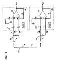
- FIGURE 2 illustrated is a simplified circuit schematic for two differential input stages for a two-line telephone instrument.
- Line 220 in FIGURE 2 represents the situation where the telephone signals received by both LINE 1 and LINE 2 are received from the same CO, and thus have the same signal reference.
- V Aout ⁇ V A
- V Bout ⁇ V B.
- V A+ V A- .
- V B+ V B- .
- V B+ V G ⁇ / (1+ ⁇ )
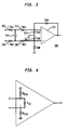
- FIGURE 3 illustrates a detailed circuit schematic of a dc-coupled differential input stage 300 which may be employed to advantage in a multi-line telephone instrument.
- differential input stage 300 may be suitably modified for ac-coupled circuit applications.
- Input stage 300 is functionally equivalent to the simplified circuits 100 illustrated in FIGURE 1 with the exception of the addition of resistors 301, 302, and with the exception that resistors R 1 and R 2 of the circuit in FIGURE 1 have each been split into two component parts, with a capacitor 310 inserted across the line between the component parts.
- the purpose of the addition of capacitor 310 is to provide high-frequency noise filtering of the differential input signal.
- Resistors 301, 302, as hereinafter described, reduce the common mode input resistance of operational amplifier 110, whereby crosscoupled interference between telephone lines is reduced in multi-line telephone instruments.
- the circuit and method of the present invention employs a means of reducing the common mode signals present at the inputs to each operational amplifier, while minimizing any effect on the differential signals received on each telephone line.
- An ideal operational amplifier is not supposed to draw any input current - that is, the signal current into the inverting and non-inverting terminals are both zero.
- the input impedance of an ideal operational amplifier is supposed to be infinite.
- presently available operational amplifiers are not ideal; they have a differential input resistance (R id ), that is the resistance as measured between the inverting and non-inverting input terminals, and a common-mode input resistance (R icm ), that can be measured by tying the inverting and non-inverting input terminals together and measuring the input resistance to ground
- FIGURE 4 illustrates the equivalent circuit of an operational amplifier, incorporating its finite differential and common mode input resistances, R id and R icm , respectively, where R icm is split into two equal parts (2 R icm ), each connected between one of the input terminals and ground.
- the differential and common mode input resistances should be as high as possible to avoid attenuation of the input signal.
- the present invention recognizes that, by reducing the common mode input resistance of the operational amplifier, a telephone line input stage amplifier can be designed that provides increased attenuation of unwanted common mode signals.
- the common mode input resistance of operational amplifier 110 is reduced by adding resistors 301, 302 between the inverting and non-inverting input terminals and ground.
- resistors 301, 302 effectively adds resistance in parallel with the effective common mode input resistances (2R icm ) internal to the operational amplifier, thus yielding a common mode input resistance of lower value.
- An undesired effect of this may be a reduction in the differential input resistance of the operational amplifier. This effect may be offset by increasing the value of series input resistors 303, 304, 305, 306.
- Component values shown in FIGURE 3 have been demonstrated experimentally to provide acceptable circuit operation while decreasing common mode interference between telephone lines in multi-line telephone instruments.
- FIGURES 5a and 5b in conjunction, illustrate the capability of the present invention to prevent common mode interference between telephone lines in multi-line telephone instruments.
- FIGURES 5a and 5b are plots of input and output voltage waveforms for first and second differential input stages, constructed as shown in FIGURE 3, in a multi-line telephone instrument employing the present invention. These plots represent the situation where LINE 1 of the multi-line phone receives a 212 volt peak (424 volt peak-to-peak) 20 Hz sine wave with a 79 volt DC component, representative of an abnormally large telephone ringing signal.
- FIGURE 5a illustrates a plot of the input and output voltage waveforms for the operational amplifier of a differential input stage for LINE 1 when an abnormally large ringing signal is received on LINE 1 of a two-line telephone instrument employing the present invention.
- plots 2 and 3 represent the voltages present at the input terminals to operational amplifier 110 of LINE 1
- plot 1 represents the voltage output of operational amplifier 110.
- the operational amplifier output voltage is clipped, meaning the amplifier is saturated. This is also reflected by the fact that the operational amplifier inputs are not tracking each other, as shown by the offset of plots 2 and 3.
- FIGURE 5b illustrates a plot of the input and output voltage waveforms for the operational amplifier of the differential input stage for LINE 2 when an abnormally large ringing signal is received on LINE 1 of a two-line telephone instrument employing the present invention.
- FIGURE 5b illustrates, even though a high-voltage ringing signal has caused the LINE 1 operational amplifier 110 to periodically saturate (reference FIGURE 5a), LINE 2 is unaffected. This is illustrated by the fact that plots 2 and 3, corresponding to the voltages at the input terminals to the operational amplifier for LINE 2, are tracking each other, signifying that the amplifier for LINE 2 does not saturate even though the amplifier for LINE 1 is periodically going into saturation.
- FIGURE 6 further illustrates the capability of the present invention to prevent common mode interference between telephone lines in multi-line telephone instruments.
- FIGURE 6 illustrates the input and output voltage waveforms for the operational amplifier of a differential input stage of LINE 2 when simultaneous calls are connected to LINE 1 and LINE 2 of a two-line telephone instrument employing the present invention, when each call is received from remote COs.
- VCO represents the difference in magnitude of signal reference potentials for LINE 1 and LINE 2 telephone signals received from different COs.
- Plots 2 and 3 illustrate the voltages present at the input terminals to the operational amplifier 110 corresponding to LINE 2, while plot 1 illustrates the output voltage of the same amplifier.
- the amplifier input voltages track each other, signifying that the amplifier does not saturate for any value of VCO ranging from -200 volts to +200 volts.
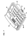
- FIGURE 7 illustrates a multi-line telephone set 100 suitable to employ the present invention.
- Telephone instrument 100 comprises a base 130 having a keypad 131 and a liquid crystal display ("LCD") 110 operating as a data display.
- LCD 110 is suitable for providing information to users such as time-of-day, dialed telephone numbers or the telephone number of an incoming call.
- a handset 140 is coupled to the base and provides an interface to a user for transmission and receipt of speech.
- a network interface 150 is couplable to multiple lines of a telecommunications network (not shown) via a telephone line (also not shown) comprising tip and ring conductors for each line.
Landscapes
- Engineering & Computer Science (AREA)
- Signal Processing (AREA)
- Telephone Function (AREA)
- Interface Circuits In Exchanges (AREA)
Applications Claiming Priority (2)
| Application Number | Priority Date | Filing Date | Title |
|---|---|---|---|
| US597756 | 1996-02-07 | ||
| US08/597,756 US5694460A (en) | 1996-02-07 | 1996-02-07 | Circuit and method for reducing common mode interference in telephone instruments |
Publications (1)
| Publication Number | Publication Date |
|---|---|
| EP0789475A2 true EP0789475A2 (fr) | 1997-08-13 |
Family
ID=24392805
Family Applications (1)
| Application Number | Title | Priority Date | Filing Date |
|---|---|---|---|
| EP97300694A Withdrawn EP0789475A2 (fr) | 1996-02-07 | 1997-02-04 | Circuit et méthode pour la réduction de interférences des mode commun dans des appareils téléphoniques |
Country Status (4)
| Country | Link |
|---|---|
| US (1) | US5694460A (fr) |
| EP (1) | EP0789475A2 (fr) |
| JP (1) | JP3212526B2 (fr) |
| CA (1) | CA2193154C (fr) |
Families Citing this family (2)
| Publication number | Priority date | Publication date | Assignee | Title |
|---|---|---|---|---|
| TW373047B (en) | 1997-04-02 | 1999-11-01 | Matsushita Electric Industrial Co Ltd | Apparatus for washing human private |
| CN102025837A (zh) * | 2009-09-17 | 2011-04-20 | 鸿富锦精密工业(深圳)有限公司 | 网间连接器及检测电话拨号连接的方法 |
Family Cites Families (3)
| Publication number | Priority date | Publication date | Assignee | Title |
|---|---|---|---|---|
| US4570034A (en) * | 1984-06-18 | 1986-02-11 | Novation, Inc. | Phone line ring signal detection circuit |
| US4803718A (en) * | 1987-03-06 | 1989-02-07 | Tree Technologies Corporation | Hold detecting and control circuit for a key telephone system |
| US5274702A (en) * | 1992-04-16 | 1993-12-28 | Northern Telecom Limited | Wideband telephone line interface circuit |
-
1996
- 1996-02-07 US US08/597,756 patent/US5694460A/en not_active Expired - Lifetime
- 1996-12-17 CA CA002193154A patent/CA2193154C/fr not_active Expired - Fee Related
-
1997
- 1997-01-31 JP JP01875197A patent/JP3212526B2/ja not_active Expired - Fee Related
- 1997-02-04 EP EP97300694A patent/EP0789475A2/fr not_active Withdrawn
Non-Patent Citations (1)
| Title |
|---|
| None |
Also Published As
| Publication number | Publication date |
|---|---|
| US5694460A (en) | 1997-12-02 |
| JPH09233180A (ja) | 1997-09-05 |
| JP3212526B2 (ja) | 2001-09-25 |
| CA2193154C (fr) | 2000-03-07 |
| CA2193154A1 (fr) | 1997-08-08 |
Similar Documents
| Publication | Publication Date | Title |
|---|---|---|
| CA1202742A (fr) | Circuit d'interface de ligne pour le declenchement par boucle et par la terre | |
| US5822426A (en) | Balanced hybrid circuit | |
| US5052039A (en) | Line interface circuit | |
| JP2850126B2 (ja) | ラインインタフェース回路 | |
| JPS61140237A (ja) | 電力線搬送通信用インターフエース回路 | |
| JP3185146B2 (ja) | 広帯域電話ライン・インタフェース回路 | |
| US5579144A (en) | Data access arrangement having improved transmit-receive separation | |
| US20020151329A1 (en) | Wireless telephone coupler | |
| US5444777A (en) | Battery feed for telephone line cards | |
| US4599491A (en) | Apparatus for converting direct coupled data devices to acoustic coupled data devices | |
| US5694460A (en) | Circuit and method for reducing common mode interference in telephone instruments | |
| US6128384A (en) | Self configuring telephone headset amplifier | |
| JPS6037860A (ja) | 電話機の改良 | |
| KR100357801B1 (ko) | 수신신호경로에서의측음감소회로 | |
| JP4289799B2 (ja) | 組込みアイソレーターを具えた低域フィルター装置と該装置を有した個人機器 | |
| US4689814A (en) | External device interface for an electronic telephone | |
| US5600713A (en) | On-board ring signal generator | |
| US4518829A (en) | Two terminal microphone active load gain regulation circuit | |
| US20050094802A1 (en) | Direct access arrangement | |
| US5337354A (en) | Tip-ring voltage correction circuit | |
| US5768367A (en) | Method and apparatus for removing FSK in-band signaling | |
| JPS6230546B2 (fr) | ||
| US6519338B2 (en) | Tone burst generator and its application to telephony | |
| US6819761B1 (en) | Programmable constant current “off hook” circuit | |
| GB2075798A (en) | Central office interface circuit |
Legal Events
| Date | Code | Title | Description |
|---|---|---|---|
| PUAI | Public reference made under article 153(3) epc to a published international application that has entered the european phase |
Free format text: ORIGINAL CODE: 0009012 |
|
| AK | Designated contracting states |
Kind code of ref document: A2 Designated state(s): DE GB |
|
| STAA | Information on the status of an ep patent application or granted ep patent |
Free format text: STATUS: THE APPLICATION HAS BEEN WITHDRAWN |
|
| 18W | Application withdrawn |
Withdrawal date: 20021120 |