EP0790607A1 - Photodetektor für optischen Kopf - Google Patents
Photodetektor für optischen Kopf Download PDFInfo
- Publication number
- EP0790607A1 EP0790607A1 EP97102451A EP97102451A EP0790607A1 EP 0790607 A1 EP0790607 A1 EP 0790607A1 EP 97102451 A EP97102451 A EP 97102451A EP 97102451 A EP97102451 A EP 97102451A EP 0790607 A1 EP0790607 A1 EP 0790607A1
- Authority
- EP
- European Patent Office
- Prior art keywords
- light
- photodetector
- optical
- receiving
- objective lens
- Prior art date
- Legal status (The legal status is an assumption and is not a legal conclusion. Google has not performed a legal analysis and makes no representation as to the accuracy of the status listed.)
- Granted
Links
- 230000003287 optical effect Effects 0.000 title claims abstract description 163
- 201000009310 astigmatism Diseases 0.000 claims description 5
- 230000004075 alteration Effects 0.000 description 5
- 230000002093 peripheral effect Effects 0.000 description 5
- 239000000758 substrate Substances 0.000 description 4
- 230000000694 effects Effects 0.000 description 3
- 238000004891 communication Methods 0.000 description 2
- 238000000034 method Methods 0.000 description 2
- 230000007423 decrease Effects 0.000 description 1
- 230000001419 dependent effect Effects 0.000 description 1
- 230000000994 depressogenic effect Effects 0.000 description 1
- 238000006073 displacement reaction Methods 0.000 description 1
- 230000009977 dual effect Effects 0.000 description 1
Images


Classifications
-
- G—PHYSICS
- G11—INFORMATION STORAGE
- G11B—INFORMATION STORAGE BASED ON RELATIVE MOVEMENT BETWEEN RECORD CARRIER AND TRANSDUCER
- G11B7/00—Recording or reproducing by optical means, e.g. recording using a thermal beam of optical radiation by modifying optical properties or the physical structure, reproducing using an optical beam at lower power by sensing optical properties; Record carriers therefor
- G11B7/12—Heads, e.g. forming of the optical beam spot or modulation of the optical beam
- G11B7/13—Optical detectors therefor
- G11B7/131—Arrangement of detectors in a multiple array
-
- G—PHYSICS
- G11—INFORMATION STORAGE
- G11B—INFORMATION STORAGE BASED ON RELATIVE MOVEMENT BETWEEN RECORD CARRIER AND TRANSDUCER
- G11B7/00—Recording or reproducing by optical means, e.g. recording using a thermal beam of optical radiation by modifying optical properties or the physical structure, reproducing using an optical beam at lower power by sensing optical properties; Record carriers therefor
- G11B7/12—Heads, e.g. forming of the optical beam spot or modulation of the optical beam
- G11B7/13—Optical detectors therefor
- G11B7/133—Shape of individual detector elements
-
- G—PHYSICS
- G11—INFORMATION STORAGE
- G11B—INFORMATION STORAGE BASED ON RELATIVE MOVEMENT BETWEEN RECORD CARRIER AND TRANSDUCER
- G11B7/00—Recording or reproducing by optical means, e.g. recording using a thermal beam of optical radiation by modifying optical properties or the physical structure, reproducing using an optical beam at lower power by sensing optical properties; Record carriers therefor
- G11B7/12—Heads, e.g. forming of the optical beam spot or modulation of the optical beam
- G11B7/135—Means for guiding the beam from the source to the record carrier or from the record carrier to the detector
- G11B7/1353—Diffractive elements, e.g. holograms or gratings
-
- G—PHYSICS
- G11—INFORMATION STORAGE
- G11B—INFORMATION STORAGE BASED ON RELATIVE MOVEMENT BETWEEN RECORD CARRIER AND TRANSDUCER
- G11B7/00—Recording or reproducing by optical means, e.g. recording using a thermal beam of optical radiation by modifying optical properties or the physical structure, reproducing using an optical beam at lower power by sensing optical properties; Record carriers therefor
- G11B2007/0003—Recording, reproducing or erasing systems characterised by the structure or type of the carrier
- G11B2007/0006—Recording, reproducing or erasing systems characterised by the structure or type of the carrier adapted for scanning different types of carrier, e.g. CD & DVD
-
- G—PHYSICS
- G11—INFORMATION STORAGE
- G11B—INFORMATION STORAGE BASED ON RELATIVE MOVEMENT BETWEEN RECORD CARRIER AND TRANSDUCER
- G11B7/00—Recording or reproducing by optical means, e.g. recording using a thermal beam of optical radiation by modifying optical properties or the physical structure, reproducing using an optical beam at lower power by sensing optical properties; Record carriers therefor
- G11B7/002—Recording, reproducing or erasing systems characterised by the shape or form of the carrier
- G11B7/0037—Recording, reproducing or erasing systems characterised by the shape or form of the carrier with discs
Definitions
- the invention relates to an optical head, and more particularly to an optical head recording data signals to and reproducing recorded data out of an optical recording medium such as a compact disk including substrates having different thicknesses.
- a widely used optical disk includes an optical head which transmits a light through a transparent substrate to thereby form a micro-spot on a plane of a recording medium in order to protect the plane fabricated in micron-order.
- a light emitted from a laser source inside the optical head is transmitted as a converging beam through a transparent substrate comprising a parallel plate of an optical disk.
- the beam is caused to have wave aberration which is dependent on a thickness of the parallel plate through which the beam has passed.
- wave aberration indicates a gap between an equiphase of a converging beam and a spherical plane. A great gap causes a converging spot to expand beyond the diffraction limit, resulting in that it is impossible to obtain good data-reproduction performance.
- a lens is designed to compensate for the wave aberration in an optical head system in order to form a micro-spot in the vicinity of the diffraction limit on a plane of a recording medium.
- an optical disk is designed to have a different thickness in accordance with what it is applied to.
- the compensation for the above mentioned wave aberration varies in dependence on a thickness of an optical disk.
- a conventional optical head has a problem that it can reproduce only data recorded in an optical disk having a specific thickness.
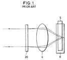
- the suggested optical head is partially illustrated in Fig. 1.
- a beam emitted from a laser source passes through a compensation holographic optical element 20 and is focused onto both a first optical disk 5 having a thickness of 0.6 mm and a second optical disk 6 having a thickness of 1.2 mm by means of an objective lens 4.
- Lights reflected at the first and second optical disks 5 and 6 pass through the objective lens 4 and then the compensation holographic optical element 20, and are received in a photodetector (not illustrated).
- the objective lens 4 is designed to be adapted for the first optical disk 5 having a thickness of 0.6 mm and reproduce data-recorded signals derived from the first optical disk 5 by means of a transmitted zero order light derived from the compensation holographic optical element 20 and having no phase changes.
- the compensation holographic optical element 20 is designed to have a grating to emit a +1st order diffracted light for compensating for aberration still existing in a light transmitting through the objective lens 4 due to a difference in a thickness between the first and second optical disks.
- the conventional head poses a problem that it is not avoidable that an efficiency of utilizing a light is reduced, and accordingly an amount of light is significantly reduced. For instance, provided that a division ratio is 50% for a transmitted zero order light and also 50% for a +1st order diffracted light, the efficiency of a light is merely 25%, because the light passes through the compensation holographic optical element 20 twice in outgoing and incoming paths.
- an object of the present invention to provide an optical head capable of recording data onto and reproducing data out of optical disks having different thicknesses with smaller reduction in an amount of a light than a conventional optical head.
- an optical head including: (a) a laser source for emitting a light; (b) an objective lens for focusing the light onto a plane of an optical recording medium; and (c) a photodetector for receiving a light reflected from the optical recording medium and passing through the objective lens, characterized by: the photodetector including a first light-receiving region for receiving a light reflected from the optical recording medium and passing through a central portion of the objective lens and a second light-receiving region for receiving a light reflected from the optical recording medium and passing through a non-central portion of the objective lens; and means for selecting one of an output signal transmitted from the first light-receiving region and a sum of output signals transmitted from the first and second light-receiving regions in accordance with a thickness of the optical recording medium.
- the optical head further includes a holographic optical element disposed in an optical path between the laser source and the objective lens for separating a first reflection light reflected from the optical recording medium and passing through a central portion of the objective lens and a second reflection light reflected from the optical recording medium and passing through a non-central portion of the objective lens from each other, the photodetector including a first light-receiving region for receiving the first reflection light and a second light-receiving region for receiving the second reflection light; and
- the first light-receiving region of the photodetector is defined as a region inside a closed boundary
- the second light-receiving region of the photodetector is defined as a region outside the closed boundary.
- the closed boundary may be a circle or an ellipse in shape.
- the ellipse preferably has a major axis extending in a direction in which the light transmitted from the laser source moves.
- the optical head may further include a beam splitter disposed in an optical path between the laser source and the objective lens for introducing a light reflected from the optical recording medium into the photodetector.
- the optical head may further include an astigmatism generating element disposed in an optical path between the beam splitter and the photodetector, a light-receiving region of the photodetector being divided into four sections, in which case the four sections of the light-receiving region are preferably equal in area to one another.
- the astigmatism generating element is comprised of a parallel plate.
- the optical head may further include a diffraction element disposed in an optical path between the laser source and the beam splitter.
- a light-receiving region of the photodetector is divided into three sections. It is preferable that these three sections are equal in area to one another.
- the first light-receiving region of the photodetector is comprised of two regions each of which is divided into two sections, and the second light-receiving region of the photodetector is comprised of a single region, the two regions and the single region being disposed in a line.
- the optical head may further include a diffraction element disposed in an optical path between the laser source and the holographic optical element, in which case a light-receiving region of the photodetector preferably includes two first regions each of which is divided into two sections and which are horizontally, adjacently disposed, two second regions each disposed above and below the first regions, and third three regions vertically disposed in a line adjacent to the first and second regions.
- a light-receiving region of the photodetector preferably includes two first regions each of which is divided into two sections and which are horizontally, adjacently disposed, two second regions each disposed above and below the first regions, and third three regions vertically disposed in a line adjacent to the first and second regions.
- the holographic optical element may have a first area through which the first reflected light passes and a second area through which the second reflected light passes, the first area including two sections defined by dividing a closed area into two areas, the second area being defined as an area outside the closed area.
- the first area is a circle in shape, and the two sections are defined by dividing the first area with aline passing a center thereof.
- the first area is preferably centrally located in the second area.
- a first light reflected from an optical recording medium and passing through a central portion of the objective lens is received at the first light-receiving region of the photodetector, and a second light reflected from an optical recording medium and passing through a peripheral portion of the objective lens is received at the second light-receiving region of the photodetector. Then, there is selectively transmitted either an output signal from the first light-receiving region or a sum of output signals from the first and second light-receiving regions in accordance with a thickness of the optical recording medium.
- the minimized reduction in a light utilization efficiency in turn advantageously decreases the reduction in an amount of a light relative to a conventional optical head.
- two optical disks having different thicknesses can be used only by dividing a light-receiving portion of a photodetector into several sections in the present invention, it is now possible to fabricate the inventive optical head with an increase in the number of optical elements being depressed.
- the holographic optical element makes it possible to independently introduce lights reflected from optical disks and passing through central and peripheral portions of an objective lens into a photodetector, and hence two optical disks having different thicknesses are allowed to use with a minor change in existing optical heads.
- Fig. 1 is a schematic view partially illustrating a conventional optical head.
- Fig. 2 is a schematic view illustrating an optical head made in accordance with the first embodiment of the present invention.
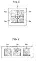
- Fig. 3 is a plan view illustrating another photodetector to be used in the optical head illustrated in Fig. 2.
- Fig. 4 is a plan view illustrating still another photodetector to be used in the optical head illustrated in Fig. 2.
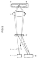
- Fig. 5 is a schematic view illustrating an optical head made in accordance with the second embodiment of the present invention.
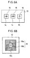
- Fig. 6A is a plan view illustrating an example of a photodetector to be used in the optical head illustrated in Fig. 5.
- Fig. 6B is a plan view illustrating an example of a holographic optical element to be used in the optical head illustrated in Fig. 5.
- Fig. 7 is a plan view illustrating another example of a photodetector to be used in the optical head illustrated in Fig. 5.
- Fig. 2 illustrates an optical head made in accordance with the first embodiment, which includes a laser source 1, a beam splitter 2, a photodetector 3, an objective lens 4, a switch 8, and an adder 9. There are disposed a first optical disk 5 having a thickness of 0.6 mm and a second optical disk having a thickness of 1.2 mm in facing relation to the objective lens 4,
- a light emitted from the laser source 1 passes through the beam splitter 2, and is focused onto a recording plane of the first optical disk 5 or the second optical disk 6 by means of the objective lens 4.
- a light reflected at the first or second optical disk 5 or 6 passes through the objective lens 4 again and is reflected at the beam splitter 2 to thereby be introduced into and received in the photodetector 3.
- the photodetector 3 has a light-receiving plane divided into two light-receiving regions: a first light-receiving region 7a which is circular in shape, and a second light-receiving region 7b which is rectangular in shape and wholly surrounds the first light-receiving region 7a.
- the first and second light-receiving regions 7a and 7b receive a light, and transform the received light into a current.
- the first light-receiving region 7a is in direct communication to the adder 9, whereas the second light-receiving region 7b is in indirect communication to the adder 9, that is, the switch 8 is provided between the second light-receiving region 7b and the adder 9.
- the switch 8 When the first optical 0.6 mm-disk 5 is to be reproduced, the switch 8 is made closed or turned on. As a result, electric signals representing a current produced by photoelectric transfer in the first and second light-receiving regions 7a and 7b are summed in the adder 9, and the adder 9 outputs a sum of the signals as a reproduction signal S.
- the reflected light passing through the objective lens 4 are wholly used to produce the reproduction signal S. This is because a light having passed through the objective lens 4 is converged into a focus on a recording plane of the first optical disk 5 after passing through a substrate of the first optical disk 5.
- the switch 8 When the second optical 1.2mm-disk 6 is to be reproduced, the switch 8 is made open or turned off. As a result, an electric signal representing a current produced by photoelectric transfer only in the first light-receiving region 7a is transmitted to the adder 9, which outputs a reproduction signal S accordingly.
- a light having passed through a central portion of the objective lens 4 forms an image on a recording plane of the second optical disk 6 which is more remote from the objective lens 4 than a recording plane of the first optical disk 5 on which a light having passed through a peripheral portion of the objective lens 4 forms an image.
- the reproduction signal S is derived only from a light having passed through a central portion of the objective lens 4 among lights reflected from the second optical disk 6 and passing through the objective lens 4.
- the first embodiment makes it possible to use two optical disk having different thicknesses only by dividing a light-receiving plane of the photodetector 3 into several regions with a slight increase in the number of optical elements.
- the division of a light is carried out only by means of a beam splitter which is included even in a conventional optical head, the reduction in an amount of a light is smaller than that of the conventional optical head illustrated in Fig. 1 employing the compensation holographic optical element 20.
- an astigmatism generating element such as a parallel plate 21 (illustrated with a broken line in Fig. 2) in an optical path between the beam splitter 2 and the photodetector 3, in which case, a light-receiving plane of the photodetector 3 is preferably divided into four sections 10a, 10b, 10c and 10d, as illustrated in Fig. 3.
- the four sections 10a to 10d are square in shape and defined by two lines passing a center of the photodetector 3 and perpendicularly intersecting with each other. Namely, the four sections 10a to 10d are equal in area to one another.
- the division of the photodetector 3 into the four sections ensures to obtain focusing error signals by astigmatism and/or tracking error signals by push-pull or heterodyne.
- a diffraction element 17 in an optical path between the laser source 1 and the beam splitter 2, in which case, a light-receiving plane of the photodetector 3 is preferably divided into three sections 11a, 11b and 11c, as illustrated in Fig. 4.
- the sections 11a to 11c are all square in shape and equal in area, and are arranged horizontally in a line. This arrangement makes it relatively easy to have tracking error signals by three beams technique.
- a combination of a collimate lens and an objective lens for introducing a laser beam emitted from the laser source 1 to the first or second optical desks 5 or 6.
- a polarized beam splitter and a quarter wavelength plate for increasing an amount of a reflected light.
- Fig. 5 illustrates an optical head made in accordance with the second embodiment of the present invention. Parts or elements corresponding to those of the first embodiment illustrated in Fig. 2 have been provided with the same reference numerals.
- the illustrated optical head includes a laser source 1, a objective lens 4, a holographic optical element 12, and a photodetector 13.
- a first light-receiving region of the photodetector 3 is comprised of two regions 14 each of which is divided into two sections, and a second light-receiving region of the photodetector 3 is comprised of a single region 15, as illustrated in Fig. 6A.
- These two regions 14 and the single region 15 are disposed horizontally in a line in the photodetector 3.
- the regions 14 and 15 are square in shape, and receive a light at a central, circular portion 16 thereof.
- the holographic optical element 12 has a first area 18 and a second area 18c, as illustrated in Fig. 6B.
- the first area 18 is circular in shape, and consists of two half-circular sections 18a and 18b defined by dividing the circular first area 18 with a line passing a center of the circular first area 18.
- the second area 18c is square in shape, and wholly surrounds the first area 18 so that the first area 18 is centrally located in the second area 18c.
- a laser beam emitted from the laser source 1 passes through the holographic optical element 12 and is focused on a recording plane of the first or second optical disk 5 or 6 by means of the objective lens 4.
- the beam reflected at the first or second optical disk 5 or 6 passes through the objective lens 4 again, and is diffracted by the holographic optical element 12 to thereby be introduced into the photodetector 13.
- the beam received in the photodetector 13 is transformed into a current, namely photoelectric transfer is carried out.
- the division of the holographic optical element 12 into the first and second areas 18 and 18c provides the same advantageous effects as the effects provided by the division of a light-receiving plane of the photodetector 3 illustrated in Fig. 2.
- the circular first area 18 of the holographic optical element 12 is further divided into the two half-circular area 18a and 18b, as illustrated in Fig. 6B, to thereby detect focusing error signals.
- the two light-receiving regions 14 of the photodetector 13 each divided into two sections receive the light diffracted at the first area 18 of the holographic optical element 12 consisting of the half-circular sections 18a and 18b, and the single light-receiving region 15 of the photodetector 13 receives the light diffracted at the square, second area 18c of the holographic optical element 12.
- the electric signals produced by photoelectric transfer carried out in the two light-receiving regions 14 are output signals representing a beam having passed through a central portion of the objective lens 4, whereas the electric signals produced by photoelectric transfer carried out in the single light-receiving region 15 are output signals representing a beam having passed through a peripheral portion of the objective lens 4.
- the first optical 0.6 mm-disk 5 is to be reproduced, there is obtained an output signal representing a sum of outputs derived from the regions 14 and 15 for the same reason as mentioned in the first embodiment.
- the second optical 1.2mm-disk 6 When the second optical 1.2mm-disk 6 is to be reproduced, for the same reason as mentioned in the first embodiment, there is obtained a reproduction signal derived only from the reflected light having passed through a central portion of the objective lens 4 and having been diffracted at the half-circular sections 18a and 18b located at the center of the holographic optical element 12 illustrated in Fig. 6B among all of the lights having been reflected from the second optical disk 6 and having passed through the objective lens 4.
- the obtained output signal is equal to a sum of output signals derived from the two half-divided light-receiving regions 14.
- the holographic optical element 12 employed in the second embodiment is an optical part similar to a beam splitter and is used for separating a beam directed from a laser source to an objective lens from a beam reflected at an optical disk and passing through an objective lens, and further for directing the latter light to a photodetector. That is, the holographic optical element 12 is different from the compensation holographic optical element 20 used in a conventional optical head as illustrated in Fig. 1 for always separating a beam directed to an optical disk into two pieces, and hence the optical head in accordance with the second embodiment enhances an efficiency of utilizing a beam relative to a conventional optical head.
- the second embodiment provides an advantage of being capable of using two optical disks having different thicknesses with a small drop in an amount of a light by dividing a light-receiving plane of the photodetector 13 into a plurality of sections and providing the holographic optical element 12.
- a light-receiving region of the photodetector 13 is preferably designed to include two first regions 19b and 19c each of which is divided into two sections, two second regions 19a and 19d, and three third regions 19e, 19f and 19g.
- the first regions 19b and 19c are horizontally, adjacently disposed.
- the second regions 19a and 19d are disposed above and below the first regions 19b and 19c, respectively.
- the third regions 19e, 19f and 19g are vertically disposed in a line and adjacent to the first and second regions 19b, 19c and 19a, 19d.
- the holographic optical element 12 can be readily combined with various means for detecting errors.
- a boundary between the first and second light-receiving regions is shaped to be a circle.
- a center of a beam also moves in a light-receiving plane, resulting in that there arises a problem that the reproduction signal characteristics are varied because of a beam displacement.
- a boundary between the first and second light-receiving regions may be shaped to be an ellipse having a major axis extending in a direction in which the beam moves. Such an elliptical boundary not only solves the problem, but also provides the same advantageous effects as those obtained by the first and second embodiments.
Landscapes
- Physics & Mathematics (AREA)
- Optics & Photonics (AREA)
- Optical Head (AREA)
- Optical Recording Or Reproduction (AREA)
Applications Claiming Priority (3)
| Application Number | Priority Date | Filing Date | Title |
|---|---|---|---|
| JP8027590A JPH09219036A (ja) | 1996-02-15 | 1996-02-15 | 光ヘッド装置 |
| JP2759096 | 1996-02-15 | ||
| JP27590/96 | 1996-02-15 |
Publications (2)
| Publication Number | Publication Date |
|---|---|
| EP0790607A1 true EP0790607A1 (de) | 1997-08-20 |
| EP0790607B1 EP0790607B1 (de) | 2000-05-10 |
Family
ID=12225174
Family Applications (1)
| Application Number | Title | Priority Date | Filing Date |
|---|---|---|---|
| EP97102451A Expired - Lifetime EP0790607B1 (de) | 1996-02-15 | 1997-02-14 | Photodetektor für optischen Kopf |
Country Status (4)
| Country | Link |
|---|---|
| US (1) | US5872759A (de) |
| EP (1) | EP0790607B1 (de) |
| JP (1) | JPH09219036A (de) |
| DE (1) | DE69701905T2 (de) |
Cited By (1)
| Publication number | Priority date | Publication date | Assignee | Title |
|---|---|---|---|---|
| EP0918321A3 (de) * | 1997-11-19 | 1999-06-16 | Samsung Electronics Co., Ltd. | Mit optischen Aufzeichnungsmedien kompatibler optischer Abtastkopf |
Families Citing this family (2)
| Publication number | Priority date | Publication date | Assignee | Title |
|---|---|---|---|---|
| US20050068864A1 (en) * | 1999-07-08 | 2005-03-31 | Samsung Electronics Co., Ltd. | Method and apparatus for tracking error detection in optical disk driver |
| DE60033017T2 (de) * | 1999-11-30 | 2007-05-10 | Matsushita Electric Industrial Co., Ltd., Kadoma | Halbleiterlaser, verfahren zu dessen herstellung und optische plattenvorrichtung |
Citations (6)
| Publication number | Priority date | Publication date | Assignee | Title |
|---|---|---|---|---|
| JPS60138748A (ja) * | 1983-12-27 | 1985-07-23 | Toshiba Corp | 光学式情報再生装置 |
| DE3913229A1 (de) * | 1988-09-19 | 1990-03-22 | Pioneer Electronic Corp | Wiedergabegeraet fuer optische informationen |
| JPH0414626A (ja) * | 1990-05-08 | 1992-01-20 | Copal Co Ltd | 光記録装置 |
| JPH06215406A (ja) * | 1993-01-13 | 1994-08-05 | Matsushita Electric Ind Co Ltd | 光ヘッド |
| JPH06259804A (ja) * | 1993-03-10 | 1994-09-16 | Matsushita Electric Ind Co Ltd | 光情報記録再生装置 |
| EP0731458A1 (de) * | 1995-03-10 | 1996-09-11 | Sony Corporation | Objektivlinse, optische Vorrichtung, und Wiedergabegerät für optische Platte |
Family Cites Families (8)
| Publication number | Priority date | Publication date | Assignee | Title |
|---|---|---|---|---|
| DE3679648D1 (de) * | 1985-12-10 | 1991-07-11 | Nec Corp | Optischer kopf mit einem beugungsgitter zum richten von zwei oder mehreren gebeugten lichtstrahlen auf optische detektoren. |
| JPS6435730A (en) * | 1987-07-31 | 1989-02-06 | Sony Corp | Focussing error detector |
| JPH01311428A (ja) * | 1988-06-09 | 1989-12-15 | Matsushita Electric Ind Co Ltd | 光ヘッド装置及びこれを用いた光情報装置 |
| JP2551302B2 (ja) * | 1991-09-18 | 1996-11-06 | 日本電気株式会社 | 光学式記録再生装置とその製造方法 |
| JP2532818B2 (ja) * | 1993-02-01 | 1996-09-11 | 松下電器産業株式会社 | 対物レンズおよび光ヘッド装置 |
| US5511059A (en) * | 1994-06-14 | 1996-04-23 | Eastman Kodak Company | Multi-element grating beam splitter with a reflection grating element for use in front facet substraction |
| KR100200858B1 (ko) * | 1995-10-04 | 1999-06-15 | 윤종용 | 광픽업장치 |
| US5659533A (en) * | 1996-07-23 | 1997-08-19 | Sampo Corporation | Method of using a single pick-up head to read and store data on discs of different thicknesses and structure of a pick-up head apparatus therefor |
-
1996
- 1996-02-15 JP JP8027590A patent/JPH09219036A/ja active Pending
-
1997
- 1997-02-14 US US08/800,855 patent/US5872759A/en not_active Expired - Fee Related
- 1997-02-14 DE DE69701905T patent/DE69701905T2/de not_active Expired - Lifetime
- 1997-02-14 EP EP97102451A patent/EP0790607B1/de not_active Expired - Lifetime
Patent Citations (6)
| Publication number | Priority date | Publication date | Assignee | Title |
|---|---|---|---|---|
| JPS60138748A (ja) * | 1983-12-27 | 1985-07-23 | Toshiba Corp | 光学式情報再生装置 |
| DE3913229A1 (de) * | 1988-09-19 | 1990-03-22 | Pioneer Electronic Corp | Wiedergabegeraet fuer optische informationen |
| JPH0414626A (ja) * | 1990-05-08 | 1992-01-20 | Copal Co Ltd | 光記録装置 |
| JPH06215406A (ja) * | 1993-01-13 | 1994-08-05 | Matsushita Electric Ind Co Ltd | 光ヘッド |
| JPH06259804A (ja) * | 1993-03-10 | 1994-09-16 | Matsushita Electric Ind Co Ltd | 光情報記録再生装置 |
| EP0731458A1 (de) * | 1995-03-10 | 1996-09-11 | Sony Corporation | Objektivlinse, optische Vorrichtung, und Wiedergabegerät für optische Platte |
Non-Patent Citations (4)
| Title |
|---|
| PATENT ABSTRACTS OF JAPAN vol. 018, no. 587 (P - 1824) 10 November 1994 (1994-11-10) * |
| PATENT ABSTRACTS OF JAPAN vol. 16, no. 167 (P - 1342) 22 April 1992 (1992-04-22) * |
| PATENT ABSTRACTS OF JAPAN vol. 18, no. 655 (P - 1844) 15 December 1994 (1994-12-15) * |
| PATENT ABSTRACTS OF JAPAN vol. 9, no. 308 (P - 410) 4 December 1985 (1985-12-04) * |
Cited By (2)
| Publication number | Priority date | Publication date | Assignee | Title |
|---|---|---|---|---|
| EP0918321A3 (de) * | 1997-11-19 | 1999-06-16 | Samsung Electronics Co., Ltd. | Mit optischen Aufzeichnungsmedien kompatibler optischer Abtastkopf |
| US6009066A (en) * | 1997-11-19 | 1999-12-28 | Samsung Electronics Co., Ltd. | Optical pickup of two different wavelength laser sources with an objective lens having an annular shielding region |
Also Published As
| Publication number | Publication date |
|---|---|
| DE69701905D1 (de) | 2000-06-15 |
| US5872759A (en) | 1999-02-16 |
| EP0790607B1 (de) | 2000-05-10 |
| JPH09219036A (ja) | 1997-08-19 |
| DE69701905T2 (de) | 2000-11-16 |
Similar Documents
| Publication | Publication Date | Title |
|---|---|---|
| US6778475B2 (en) | Optical detector, optical pickup and optical information reproducing apparatus using optical pickup for detecting at least three light beams separated from one or more light sources | |
| US6125087A (en) | Optical pickup for optical disk apparatus | |
| US6392977B2 (en) | Optical pickup with a hologram to limit the aperture of two light beams with different wavelengths | |
| US20020064121A1 (en) | Optical pickup device applicable to two kinds of recording media with minimized deterioration of a beam spot | |
| US5301182A (en) | Optical pickup head | |
| US6636464B1 (en) | Optical pickup device capable of detecting stable error signal | |
| US6377520B2 (en) | Robust and versatile focus/tracking method and system for optical pickup heads | |
| EP0790607B1 (de) | Photodetektor für optischen Kopf | |
| US5708641A (en) | Multiple focus optical pickup system | |
| TW382704B (en) | Method for focusing and tracking of CD optical head and device therefor | |
| US5684780A (en) | Optical pickup device having optical element exhibiting polarized light selectivity loaded thereon and optical apparatus having the optical pickup device loaded thereon | |
| JPH1040567A (ja) | 光学ヘッドおよびそれを用いた光学的情報再生装置 | |
| JPS6352342A (ja) | 光ピツクアツプ | |
| KR100601612B1 (ko) | 안정된 트랙킹이 가능한 광픽업장치 | |
| JP2636245B2 (ja) | 光磁気記憶用光ヘッド | |
| KR100224896B1 (ko) | 광이용 효율을 높인 광 픽업 장치 | |
| JPS62217425A (ja) | 光ヘツド装置 | |
| KR19990049993A (ko) | 광량조절을 이용한 듀얼 포커스 광픽업장치 | |
| KR20000003530A (ko) | 듀얼포커스 전용 복합렌즈가 구비된 광픽업장치 | |
| KR19990050011A (ko) | 액정소자를 이용한 듀얼 포커스 광픽업장치 | |
| KR19990050013A (ko) | 반사형 액정소자를 이용한 듀얼 포커스 광픽업장치 | |
| KR19990050001A (ko) | 광투과반사를 이용한 듀얼 포커스 광픽업장치 | |
| JPH1173674A (ja) | 光ヘッド装置 | |
| KR19990049995A (ko) | 광조절 액정소자를 이용한 듀얼 포커스 광픽업장치 | |
| KR19980058055A (ko) | 광 픽업 장치 |
Legal Events
| Date | Code | Title | Description |
|---|---|---|---|
| PUAI | Public reference made under article 153(3) epc to a published international application that has entered the european phase |
Free format text: ORIGINAL CODE: 0009012 |
|
| 17P | Request for examination filed |
Effective date: 19970610 |
|
| AK | Designated contracting states |
Kind code of ref document: A1 Designated state(s): DE FR NL |
|
| GRAG | Despatch of communication of intention to grant |
Free format text: ORIGINAL CODE: EPIDOS AGRA |
|
| 17Q | First examination report despatched |
Effective date: 19990112 |
|
| GRAG | Despatch of communication of intention to grant |
Free format text: ORIGINAL CODE: EPIDOS AGRA |
|
| GRAG | Despatch of communication of intention to grant |
Free format text: ORIGINAL CODE: EPIDOS AGRA |
|
| GRAH | Despatch of communication of intention to grant a patent |
Free format text: ORIGINAL CODE: EPIDOS IGRA |
|
| GRAH | Despatch of communication of intention to grant a patent |
Free format text: ORIGINAL CODE: EPIDOS IGRA |
|
| GRAA | (expected) grant |
Free format text: ORIGINAL CODE: 0009210 |
|
| AK | Designated contracting states |
Kind code of ref document: B1 Designated state(s): DE FR NL |
|
| REF | Corresponds to: |
Ref document number: 69701905 Country of ref document: DE Date of ref document: 20000615 |
|
| ET | Fr: translation filed | ||
| PLBE | No opposition filed within time limit |
Free format text: ORIGINAL CODE: 0009261 |
|
| STAA | Information on the status of an ep patent application or granted ep patent |
Free format text: STATUS: NO OPPOSITION FILED WITHIN TIME LIMIT |
|
| 26N | No opposition filed | ||
| PGFP | Annual fee paid to national office [announced via postgrant information from national office to epo] |
Ref country code: FR Payment date: 20100223 Year of fee payment: 14 |
|
| PGFP | Annual fee paid to national office [announced via postgrant information from national office to epo] |
Ref country code: DE Payment date: 20100226 Year of fee payment: 14 |
|
| PGFP | Annual fee paid to national office [announced via postgrant information from national office to epo] |
Ref country code: NL Payment date: 20100218 Year of fee payment: 14 |
|
| REG | Reference to a national code |
Ref country code: NL Ref legal event code: V1 Effective date: 20110901 |
|
| REG | Reference to a national code |
Ref country code: FR Ref legal event code: ST Effective date: 20111102 |
|
| PG25 | Lapsed in a contracting state [announced via postgrant information from national office to epo] |
Ref country code: NL Free format text: LAPSE BECAUSE OF NON-PAYMENT OF DUE FEES Effective date: 20110901 |
|
| PG25 | Lapsed in a contracting state [announced via postgrant information from national office to epo] |
Ref country code: FR Free format text: LAPSE BECAUSE OF NON-PAYMENT OF DUE FEES Effective date: 20110228 |
|
| REG | Reference to a national code |
Ref country code: DE Ref legal event code: R119 Ref document number: 69701905 Country of ref document: DE Effective date: 20110901 |
|
| PG25 | Lapsed in a contracting state [announced via postgrant information from national office to epo] |
Ref country code: DE Free format text: LAPSE BECAUSE OF NON-PAYMENT OF DUE FEES Effective date: 20110901 |