EP0790635A2 - Vorrichtung zur chemischen Abscheidung aus der Dampfphase mit einer getrennten Injektion von Reinigungsgas - Google Patents
Vorrichtung zur chemischen Abscheidung aus der Dampfphase mit einer getrennten Injektion von Reinigungsgas Download PDFInfo
- Publication number
- EP0790635A2 EP0790635A2 EP97200281A EP97200281A EP0790635A2 EP 0790635 A2 EP0790635 A2 EP 0790635A2 EP 97200281 A EP97200281 A EP 97200281A EP 97200281 A EP97200281 A EP 97200281A EP 0790635 A2 EP0790635 A2 EP 0790635A2
- Authority
- EP
- European Patent Office
- Prior art keywords
- reaction chamber
- coil
- clean gas
- gas injection
- plasma
- Prior art date
- Legal status (The legal status is an assumption and is not a legal conclusion. Google has not performed a legal analysis and makes no representation as to the accuracy of the status listed.)
- Withdrawn
Links
Images


Classifications
-
- H—ELECTRICITY
- H01—ELECTRIC ELEMENTS
- H01J—ELECTRIC DISCHARGE TUBES OR DISCHARGE LAMPS
- H01J37/00—Discharge tubes with provision for introducing objects or material to be exposed to the discharge, e.g. for the purpose of examination or processing thereof
- H01J37/32—Gas-filled discharge tubes
- H01J37/32431—Constructional details of the reactor
- H01J37/32798—Further details of plasma apparatus not provided for in groups H01J37/3244 - H01J37/32788; special provisions for cleaning or maintenance of the apparatus
- H01J37/32853—Hygiene
- H01J37/32862—In situ cleaning of vessels and/or internal parts
-
- H—ELECTRICITY
- H10—SEMICONDUCTOR DEVICES; ELECTRIC SOLID-STATE DEVICES NOT OTHERWISE PROVIDED FOR
- H10P—GENERIC PROCESSES OR APPARATUS FOR THE MANUFACTURE OR TREATMENT OF DEVICES COVERED BY CLASS H10
- H10P14/00—Formation of materials, e.g. in the shape of layers or pillars
- H10P14/20—Formation of materials, e.g. in the shape of layers or pillars of semiconductor materials
-
- C—CHEMISTRY; METALLURGY
- C23—COATING METALLIC MATERIAL; COATING MATERIAL WITH METALLIC MATERIAL; CHEMICAL SURFACE TREATMENT; DIFFUSION TREATMENT OF METALLIC MATERIAL; COATING BY VACUUM EVAPORATION, BY SPUTTERING, BY ION IMPLANTATION OR BY CHEMICAL VAPOUR DEPOSITION, IN GENERAL; INHIBITING CORROSION OF METALLIC MATERIAL OR INCRUSTATION IN GENERAL
- C23C—COATING METALLIC MATERIAL; COATING MATERIAL WITH METALLIC MATERIAL; SURFACE TREATMENT OF METALLIC MATERIAL BY DIFFUSION INTO THE SURFACE, BY CHEMICAL CONVERSION OR SUBSTITUTION; COATING BY VACUUM EVAPORATION, BY SPUTTERING, BY ION IMPLANTATION OR BY CHEMICAL VAPOUR DEPOSITION, IN GENERAL
- C23C16/00—Chemical coating by decomposition of gaseous compounds, without leaving reaction products of surface material in the coating, i.e. chemical vapour deposition [CVD] processes
- C23C16/44—Chemical coating by decomposition of gaseous compounds, without leaving reaction products of surface material in the coating, i.e. chemical vapour deposition [CVD] processes characterised by the method of coating
- C23C16/4401—Means for minimising impurities, e.g. dust, moisture or residual gas, in the reaction chamber
- C23C16/4405—Cleaning of reactor or parts inside the reactor by using reactive gases
-
- H—ELECTRICITY
- H01—ELECTRIC ELEMENTS
- H01J—ELECTRIC DISCHARGE TUBES OR DISCHARGE LAMPS
- H01J37/00—Discharge tubes with provision for introducing objects or material to be exposed to the discharge, e.g. for the purpose of examination or processing thereof
- H01J37/32—Gas-filled discharge tubes
- H01J37/32431—Constructional details of the reactor
- H01J37/3244—Gas supply means
-
- Y—GENERAL TAGGING OF NEW TECHNOLOGICAL DEVELOPMENTS; GENERAL TAGGING OF CROSS-SECTIONAL TECHNOLOGIES SPANNING OVER SEVERAL SECTIONS OF THE IPC; TECHNICAL SUBJECTS COVERED BY FORMER USPC CROSS-REFERENCE ART COLLECTIONS [XRACs] AND DIGESTS
- Y10—TECHNICAL SUBJECTS COVERED BY FORMER USPC
- Y10S—TECHNICAL SUBJECTS COVERED BY FORMER USPC CROSS-REFERENCE ART COLLECTIONS [XRACs] AND DIGESTS
- Y10S156/00—Adhesive bonding and miscellaneous chemical manufacture
- Y10S156/916—Differential etching apparatus including chamber cleaning means or shield for preventing deposits
Definitions
- This invention relates to chemical vapor deposition (CVD) systems and in particular to arrangements for cleaning high-density-plasma CVD systems.
- Plasma-assisted chemical vapor deposition systems are used to grow thin films on silicon wafers and other substrates. In the course of growing the film on the wafer or other substrate, the film is also deposited on other locations in the reaction chamber. Periodically, these deposits must be removed to prevent them from building up to the point where particulates are generated. Particulates can, for example, reduce microelectronic device yield, since a die on which a particle has landed during processing must normally be discarded.
- NF 3 can be used as a clean gas.
- the NF 3 plasma creates fluorine radicals which react with the SiO 2 film under the influence of ion bombardment to form SiF 4 and other volatile compounds.
- the process gas is injected into the reaction chamber through a process gas injection system, which may include a plurality of tubes.
- the deposition gas tubes may be directed radially inward from the periphery of the reaction chamber, although other orientations of the tubes are possible.
- an unwanted film of the deposition material forms on the inner surfaces of the deposition gas tubes. This film must be removed during cleaning.
- the conventional practice is to inject the clean gas through the same tubes that were used to introduce the process gas.
- a problem with this technique is that it has been found to be a very inefficient way of removing the film which forms on the insides of the deposition gas tubes.
- Fluorine-bearing compounds are frequently used as the clean gas. Following the clean cycle, a fluorine residue remains on the walls and other surfaces of the reaction chamber. The fluorine residue must be removed for safety reasons and to insure that the film adheres to the reaction chamber surfaces in the subsequent deposition cycle.
- U.S. Patent No. 5,129,958 describes the use of a reducing gas to remove the fluorine residues, but this process requires the use of elevated reaction chamber temperature, which is difficult for many systems, and therefore takes an undue amount of time.
- a plasma-enhanced chemical vapor deposition system includes at least one dedicated clean gas injection orifice or tube.
- the dedicated orifice or tube is placed at a location where minimal deposition occurs during the operation of the CVD system.
- the process gas is injected into the reaction chamber through a plurality of tubes.
- the dedicated clean gas injection orifice or tube is located between the wafer supporting chuck or platen and the outer wall of the reaction chamber, and at level approximately equal to the level of the wafer supporting chuck or platen when a wafer is being processed in the reaction chamber. This position is chosen to minimize deposition on the clean injector, minimize particle generation from the clean injector, and maintain the ability to effectively clean surfaces near the clean injector.
- the dedicated clean gas injection orifice or tube is also positioned so that it directs the clean gas to the film-coated surfaces of the reaction chamber before the clean gas reaches the exhaust pump port.
- a hemispherically-shaped coil is used to inductively couple energy to the plasma.
- the top of the coil is typically connected to a power source while the bottom of the coil (the circumferential turn of the hemisphere) is grounded.
- both the top and bottom of the coil are driven by a power source, and the coil as a whole acts to couple energy, mainly capacitively, into the plasma.
- typically the coil is operated at a significantly higher frequency during the cleaning cycle than during processing. With these modifications, the coil produces a plasma which is particularly well suited to cleaning the inside surfaces of the reaction chamber.
- the geometry of the coil is such that electrical self-resonances occur at the higher frequencies. It is believed that this property of the coil makes this electrical configuration robust for powering cleaning plasmas of varying compositions and, therefore, varying electrical characteristics.
- a plasma of hydrogen or a hydrogen-oxygen mixture is used to remove fluorine-bearing residues from the surfaces of the reaction chamber following the clean cycle.
- the use of the plasma makes the fluorine removal possible at low temperatures (25°-100° C).
- Fig. 1 is a cross-sectional view of a high-density-plasma chemical vapor deposition (HDP-CVD) system in accordance with this invention.
- HDP-CVD high-density-plasma chemical vapor deposition
- Fig. 2 is a perspective view of the lower portion of the HDP-CVD system shown in Fig. 1.
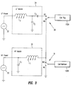
- Fig. 3 is a schematic diagram of the electrical circuitry for supplying power to the coil in the HDP-CVD system shown in Figs. 1 and 2.
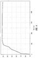
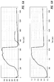
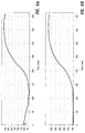
- Figs. 4, 5A, 5B, 6A and 6B are graphs showing optical emission spectroscopy (OES) scans which illustrate the results of a series of comparative tests between conventional cleaning processes and a cleaning process using a HDP-CVD system according to this invention.
- OES optical emission spectroscopy
- HDP-CVD system 10 is shown in cross-sectional view in Fig. 1.
- a perspective view of the lower portion of HDP-CVD system 10 is shown in Fig. 2.
- HDP-CVD system 10 includes an aluminum housing 100 and a hemispherical induction coil 102 that is provided in an expanding spiral pattern on six winding forms -- only forms 104 and 106 are illustrated for clarity. Six forms are used to simplify assembly of the induction coil 102, although other form types such as a unitary form are suitable as well, depending on the manufacturing techniques employed.
- the winding forms, e.g. forms 104 and 106 are made of any suitable material, which include dielectric materials such as nylon.
- the induction coil 102 is held in place inside channels in the winding forms, e.g.
- induction coil 102 is a nearly complete hemisphere in Fig. 1, alternatively the induction coil could be in the shape of a partial or truncated hemisphere.
- the induction coil 102 is made of copper tubing having an inner diameter of 3.6 mm and an outer diameter of 6.4 mm.
- the expanding spiral pattern of the induction coil 102 has 21 windings.
- the first winding is nearly coplanar with a semiconductor wafer 108, which is shown in position for processing.
- the induction coil 102 is positioned around a reaction chamber 110 which is formed by an aluminum oxide (Al 2 O 3 ) vessel or bell jar 112 in conjunction with an aluminum top plate 114.
- the vessel 112 is hemispherically shaped so that there is a balanced coupling of rf (uniform dielectric spacing) into the vacuum cavity.
- the vessel material is an insulating dielectric having sufficient structural integrity to withstand a vacuum.
- suitable materials include quartz, pyrex, polyamide, and other oxide or nitride composites.
- the induction coil 102 follows the hemispherical contour of the vessel 112, which is capable of holding a vacuum and contains the substrate, illustratively a semiconductor wafer containing integrated circuit chips in fabrication.
- the housing 100 is mounted onto the top plate 114 in any convenient manner.
- Fig. 1 shows the housing 100 as being engaged by an rf seal 116, which includes copper leaves to prevent spurious rf emissions from the HDP-CVD system 10.
- Wafer 108 is supported within the reaction chamber 110, preferably by an electrostatic chuck of the kind described in the above-referenced U.S. Application Serial No. 08/602,432 which includes a platen 118.
- the platen 118 is capable of vertical motion, which is imparted by any suitable mechanism (not shown).
- the position of the platen depends on whether the HDP-CVD system 10 is operating in process mode or in wafer transfer mode.
- the position of platen 118 in the process mode is shown in dashed lines; its position in the wafer transfer mode is shown in solid lines.
- Bellows 120 which is provided to isolate the mechanical components of the pedestal drive system at atmospheric pressure from the vacuum in reaction chamber 110, is extended. The wafer then rests on the platen 118 within the reaction chamber 110.
- the platen 118 is lowered into a wafer transfer region 122, which includes at one end a sealable wafer transfer opening 124.
- the bellows 120 is compressed, and three lifter pins (not shown) protrude through holes (not shown) in the platen 118 so as to support the wafer in a stationary position within the transfer region 122 as the platen 118 lowers.
- the sealable wafer transfer opening 124 is provided to permit a wafer transport arm (not shown) access to the transfer region 122 during wafer transfer mode. Suitable wafer transport arms and associated mechanisms are well known in the art.
- a vacuum pumping system (not shown) of any suitable type is connected to the transfer region 122 through a vacuum pump port 126 for evacuating the reaction chamber 30. Suitable vacuum pumping systems are well known in the art.
- a plurality of process gas injection tubes 128 are arrayed around the periphery of the reaction chamber 110. Tubes 128 are arranged radially and are directed inwardly and upwardly towards the top of the hemispherical vessel 112. The openings of the tubes 128 are positioned somewhat above the level of the wafer 108 when it is in position for processing. Tubes 128 are connected in a known manner to lines which supply process gases to the interior of reaction chamber 110.
- the configuration of process gas injection tubes 128 shown in Figs. 1 and 2 is determined by the particular processes that are to be performed by HDP-CVD system 10 and by the way in which the process gas is to be distributed over the wafer.
- the embodiment shown is one possible process gas injection tube configuration for using silane, O 2 and Ar to deposit a film of SiO 2 .
- the process gas injection tubes could be of a different length from the process gas tubes 128, or they could be oriented parallel to the wafer or pointed downward.
- a clean gas injector 129 Separate from the process gas injection tubes 128 is a clean gas injector 129, which includes a clean gas injection tube 130 which is made of aluminum and extends from a clean gas fitting 131 at the side of system 10. While clean gas injection tube 130 appears as if it lies in a single vertical plane in Fig. 1, Fig. 2 shows that clean gas injection tube 130 actually bends around backwards so that it approaches platen 118 between the process gas injection tubes labeled 128A and 128B in Figs. 1 and 2.
- Clean gas injector 129 also includes a ceramic (Al 2 O 3 ) sleeve 133 surrounding a portion of clean gas injection tube 130 to prevent the plasma from attacking the aluminum.
- the tip of ceramic sleeve 133 which forms the outlet of the clean gas injector 129, is located just above the level of the wafer 108 when it is in position for processing, but in other embodiments the outlet of the clean gas injector could be located at a somewhat higher or lower level.
- Clean gas injector 129 is directed upward and towards the highest point within reaction chamber 110. The outlet of the clean gas injector should be located radially outside the periphery of the wafer.
- Process gas injection tubes 128 typically are exposed to the plasma. As a result, when a wafer is being processed deposition normally occurs on the exterior and interior surfaces of the tubes 128.
- the conventional practice is to introduce the clean gas through tubes 128.
- NF 3 may be used as a clean gas.
- the NF 3 produces fluorine radicals which react with SiO 2 under simultaneous ion bombardment to form SiF 4 and other volatile compounds and thereby remove the unwanted SiO 2 film.
- the flow of the clean gas through process gas injection tubes 128 inhibits the ability of the clean gas (in this case the fluorine radicals) to reach the interior surfaces of the process gas injection tubes 128, and therefore the cleaning process is very inefficient in these locations. It has been found that, using this technique, the tubes can be cleaned only by introducing the clean gas at a very low flow rate, and even then the cleaning takes place very slowly. At higher flow rates, the tubes may not be cleaned at all.
- the clean gas injector 129 is preferably positioned at a location where minimal deposition occurs during the deposition processing cycle of the system 10. This would normally be at or below the level of the wafer during processing, but there may be other regions in the reaction chamber where the clean gas injection tube can be located.
- the dedicated clean gas injector is positioned so that it directs the clean gas to the surfaces of the reaction chamber before reaching the exhaust pump port.
- the clean gas injector should inject the clean gas at a point which is no closer than about 1 cm to surrounding surfaces. Surfaces which are less than about 1 cm from the point at which the clean gas is injected may not be effectively cleaned.
- While the clean gas injector 129 shown in Figs. 1 and 2 includes only one clean gas injection tube 130, other embodiments may include a plurality of clean gas injection tubes.
- the hemispherical coil shown in Figs. 1 and 2 is particularly useful in generating a high density plasma.
- High density plasmas e.g., 10 11 -10 13 ions/cm 3
- low pressures e.g., 0.1-100 mTorr
- the coil is driven by connecting a low-frequency rf source (e.g., in the range of 450 kHz) to the upper terminal of the coil and connecting the lower terminal of the coil to ground.
- Circuitry for driving the coil 102 is shown in Fig. 3.
- the upper terminal 102A and lower terminal 102B of coil 102 are connected through vacuum relay switches 30 and 31 to a low-frequency rf source 32 and a high-frequency rf source 33.
- low-frequency source 32 delivers an output at 350-450 kHz
- high-frequency source 33 delivers an output at 5-20 MHz and in this case at 13.56 MHz.
- the signal output of rf source 32 is fed through a low-frequency impedance matching network 34, containing an inductor L2 (7 ⁇ H) and capacitors C2 (12nF) and C3 (4.0-5.7 nF), and the signal output of rf source 33 is fed through a high-frequency matching network 35, containing a inductor L1 (0.95 ⁇ H) and a capacitor C1 (200 pF).
- the values of capacitors C1-C3 and inductors L1-L2 may be varied.
- Switches 30 and 31 are single pole, double-throw switches and are ganged together. During deposition processing, switches 30 and 31 are in the Normal Closed (NC) positions. Thus, as described above, the 450 kHz source 32 is connected to the upper terminal 102A of coil 102, and the lower terminal 102B of coil 102 is grounded. During cleaning, switches 30 and 31 are both in the Normal Open (NO) positions, and as a result the 13.56 MHz source is connected to both of the terminals 102A and 102B. In this condition, the coil 102 acts mainly through capacitive coupling to produce a plasma which is particularly suitable for cleaning the interior surfaces of reaction chamber 110.
- NC Normal Closed
- the rf signal was introduced at the terminals of the coil, in other embodiments the rf signal could be introduced at two or more other locations on the coil, e.g., at one terminal and at the midpoint of the coil, with the other terminal left floating.
- the high frequency power introduced at two or more locations on the coil can be used to create a high-density plasma, mainly by induction coupling.
- This plasma is suitable of deposition processing.
- the clean gas is frequently a fluorine bearing compound such as NF 3 , C 2 F 6 , C 3 F 8 , SF 6 , or CF 4 (possibly with the addition of O 2 , H 2 or inert gases) which as described above is activated in a glow discharge.
- the deposits are removed as volatile fluorides and oxygen.
- residual fluorine and fluorine compounds will remain adsorbed to the surfaces of the reaction chamber. If these residues are not removed, subsequent film deposits may not adhere to the surfaces of the reaction chamber, resulting in flaking and increased particulate generation. Also, operating personnel may be exposed to excessive fluorine levels if the reaction chamber is vented to the atmosphere and opened.
- the pressure in the reaction chamber pressure by a factor of 2-3 over the starting value (without the plasma). As the process continues, the pressure falls, eventually reaching the starting value. Following a eight-minute clean cycle, the process generally takes about two minutes. If the hydrogen is mixed with oxygen, the time required for the process is reduced by 33% to 50%.
- the hydrogen can be introduced at a flow rate of 50-1000 sccm, with oxygen at a flow rate of 0-500 sccm.
- the starting pressure in the reaction chamber can be in the range 0.1-5 Torr.
- the coil can be energized with an rf signal having a frequency of 150 kHz to 13.56 Mhz at a power of 500-5000 W.
- the effective cleaning rate was defined as the total thickness of film deposited on wafers, using the system in the deposition mode, divided by the time required to subsequently clean the reaction chamber.
- a goal of the plasma clean is to remove film from the surfaces of the reaction chamber periodically so that this film does not flake off and cause high particle counts on wafers.
- a high cleaning rate is desirable to maximize the number of wafers per hour that the system can process.
- NF 3 was used as the clean gas to remove a SiO 2 film.
- the time required to clean the reaction chamber was monitored by optical emission spectroscopy (OES).
- OES optical emission spectroscopy
- the intensity of light of a certain wavelength in the emission spectrum of fluorine is measured, the intensity being directly proportional to the concentration of fluorine radicals in the plasma.
- the fluorine radicals are responsible for the removal of the SiO 2 film from the reaction chamber surfaces.
- the optical emission intensity of fluorine is relatively low.
- the optical emission measurement provides an indication of the effective clean rate.
- the effective clean rate does not provide complete information about the effectiveness of the plasma clean.
- the endpoint of the optical emissions may occur without the film having been completely removed from all areas of the reaction chamber.
- the clean gas is introduced through the process gas injection tubes, the film may not be entirely removed from the interior surfaces of the tubes. Therefore, to provide a complete test result, visual inspection of all reaction chamber surfaces was made to determine which cleaning method and conditions provide the best results.
- the stability and uniformity of the clean plasma were visually observed. Poor stability and uniformity of the plasma can lead to nonuniform removal of the film in different areas of the reaction chamber. In this case, the reaction chamber materials can suffer enhanced attack in areas the film removal rate is high, and this can lead to increased contamination of the wafers and the need for more frequent maintenance of the reaction chamber.
- Test #1 the coil was energized at a low frequency (350-450 kHz) and 2 kW. The signal was applied to the upper terminal of the coil, and the lower terminal of the coil was grounded.
- Fig. 4 illustrates an OES scan of a clean cycle under these conditions with the NF 3 clean gas being introduced at 600 sccm and at a pressure of 1.6 Torr. A wavelength of 686 nm was measured.
- the effective cleaning rate of the plasma clean was fairly good (8000 A/min), and the clean was completed in about 400 seconds. The effective clean rate was not very meaningful, however, because not all surfaces of the reaction chamber (in particular the inside surfaces of the process gas injection tubes) were cleaned. Particle counts on wafers processed following the clean were unacceptable. Also, the plasma stability and uniformity were poor in Test #1.
- Fig. 5A shows an OES scan at 704 nm
- Fig. 5B shows an OES scan at 686 nm.
- the clean gas (NF 3 ) was introduced through the process gas injection tubes at a pressure of 1.5 Torr.
- a high flow rate of clean gas 800 sccm
- the flow rate of the NF 3 was reduced to 100 sccm. This was in recognition of the fact that the high flow rate of the clean gas through the process gas injection tubes prevents proper cleaning of the interior surfaces of those tubes.
- the power supplied to the coil was a 13.56 MHz signal at 4kW.
- the signal was applied to both terminals of the coil.
- This high frequency signal provided a substantially different voltage signal in the coil as compared with the low frequency signal used in Test #1.
- the high-frequency power provided improved plasma stability and uniformity.
- the high-frequency (capacitive) power coupling occurred at a relatively low maximum voltage. This reduces the intensity of the plasma attack on the reaction chamber materials themselves. However, the overall clean rate of only 3400 A/min was mediocre.
- Test #3 is illustrated in the OES scans of Figs. 6A and 6B, Fig. 6A being at a wavelength of 704 nm and Fig. 6B being at a wavelength of 686 nm.
- the clean gas was introduced through a separate clean gas injection tube, in accordance with this invention.
- the clean gas injection tube was located in a position where it received minimal deposition during processing yet delivered the clean gas (NF 3 ) to surfaces of the reaction chamber which receive substantial deposition.
- the flow rate of the clean gas was 1000 sccm at a pressure of 2 Torr.
- the power input to the coil was 13.56 MHz at 4 kW.
- the effective clean rate was 12000 A/min; all surfaces of the reaction chamber (including the process gas injection tubes) were effectively cleaned; and the stability and uniformity of the plasma were good. Other tests have shown that less advantageous positioning of the clean gas injection tube gives a lower effective rate of cleaning but still successfully cleans all surfaces of the reaction chamber.
Landscapes
- Chemical & Material Sciences (AREA)
- Engineering & Computer Science (AREA)
- Physics & Mathematics (AREA)
- Analytical Chemistry (AREA)
- Plasma & Fusion (AREA)
- Materials Engineering (AREA)
- Metallurgy (AREA)
- Organic Chemistry (AREA)
- Mechanical Engineering (AREA)
- Chemical Kinetics & Catalysis (AREA)
- General Chemical & Material Sciences (AREA)
- Health & Medical Sciences (AREA)
- Epidemiology (AREA)
- Public Health (AREA)
- Chemical Vapour Deposition (AREA)
- Drying Of Semiconductors (AREA)
- Cleaning Or Drying Semiconductors (AREA)
Applications Claiming Priority (2)
| Application Number | Priority Date | Filing Date | Title |
|---|---|---|---|
| US08/602,641 US6200412B1 (en) | 1996-02-16 | 1996-02-16 | Chemical vapor deposition system including dedicated cleaning gas injection |
| US602641 | 1996-02-16 |
Publications (2)
| Publication Number | Publication Date |
|---|---|
| EP0790635A2 true EP0790635A2 (de) | 1997-08-20 |
| EP0790635A3 EP0790635A3 (de) | 1998-04-15 |
Family
ID=24412185
Family Applications (1)
| Application Number | Title | Priority Date | Filing Date |
|---|---|---|---|
| EP97200281A Withdrawn EP0790635A3 (de) | 1996-02-16 | 1997-02-05 | Vorrichtung zur chemischen Abscheidung aus der Dampfphase mit einer getrennten Injektion von Reinigungsgas |
Country Status (7)
| Country | Link |
|---|---|
| US (1) | US6200412B1 (de) |
| EP (1) | EP0790635A3 (de) |
| JP (1) | JP3141929B2 (de) |
| KR (1) | KR100269559B1 (de) |
| DE (1) | DE790635T1 (de) |
| SG (1) | SG76499A1 (de) |
| TW (1) | TW289836B (de) |
Cited By (10)
| Publication number | Priority date | Publication date | Assignee | Title |
|---|---|---|---|---|
| WO1999020812A1 (en) * | 1997-10-21 | 1999-04-29 | Applied Materials, Inc. | Method for cleaning an etching chamber |
| WO1999062308A1 (en) * | 1998-05-22 | 1999-12-02 | Central Research Laboratories Limited | Apparatus for coupling power into a body of gas |
| EP1154036A1 (de) * | 2000-05-12 | 2001-11-14 | Applied Materials, Inc. | Gasreaktionen zum Eliminieren von Verunreinigungen in einer CVD-Reaktionskammer |
| EP1154038A1 (de) * | 2000-05-12 | 2001-11-14 | Applied Materials, Inc. | Verfahren zum Konditionieren von einem CVD Reaktionskammer |
| US6320316B1 (en) * | 1999-05-19 | 2001-11-20 | Central Research Laboratories, Limited | Apparatus for coupling power into a body of gas |
| US6450117B1 (en) | 2000-08-07 | 2002-09-17 | Applied Materials, Inc. | Directing a flow of gas in a substrate processing chamber |
| US6676760B2 (en) | 2001-08-16 | 2004-01-13 | Appiled Materials, Inc. | Process chamber having multiple gas distributors and method |
| US6797188B1 (en) | 1997-11-12 | 2004-09-28 | Meihua Shen | Self-cleaning process for etching silicon-containing material |
| WO2009036722A3 (de) * | 2007-09-21 | 2009-05-28 | Khs Corpoplast Gmbh & Co Kg | Vorrichtung zur plasmabehandlung von werkstücken |
| CN103510064A (zh) * | 2012-06-15 | 2014-01-15 | 中微半导体设备(上海)有限公司 | 真空处理装置及控制制程颗粒沉积路径的方法 |
Families Citing this family (129)
| Publication number | Priority date | Publication date | Assignee | Title |
|---|---|---|---|---|
| US6070551A (en) | 1996-05-13 | 2000-06-06 | Applied Materials, Inc. | Deposition chamber and method for depositing low dielectric constant films |
| US6184158B1 (en) * | 1996-12-23 | 2001-02-06 | Lam Research Corporation | Inductively coupled plasma CVD |
| JP3141827B2 (ja) * | 1997-11-20 | 2001-03-07 | 日本電気株式会社 | 半導体装置の製造方法 |
| US6093655A (en) | 1998-02-12 | 2000-07-25 | Micron Technology, Inc. | Plasma etching methods |
| US6235213B1 (en) | 1998-05-18 | 2001-05-22 | Micron Technology, Inc. | Etching methods, methods of removing portions of material, and methods of forming silicon nitride spacers |
| US6185839B1 (en) * | 1998-05-28 | 2001-02-13 | Applied Materials, Inc. | Semiconductor process chamber having improved gas distributor |
| US6277759B1 (en) * | 1998-08-27 | 2001-08-21 | Micron Technology, Inc. | Plasma etching methods |
| US6500771B1 (en) * | 2000-01-31 | 2002-12-31 | Chartered Semiconductor Manufacturing Ltd. | Method of high-density plasma boron-containing silicate glass film deposition |
| US6592710B1 (en) * | 2001-04-12 | 2003-07-15 | Lam Research Corporation | Apparatus for controlling the voltage applied to an electrostatic shield used in a plasma generator |
| KR100443905B1 (ko) * | 2001-03-23 | 2004-08-09 | 삼성전자주식회사 | 화학 기상 증착장치 |
| US20020163632A1 (en) * | 2001-05-02 | 2002-11-07 | Ya-Chan Cheng | Measuring system of a gas stream environment |
| US6815362B1 (en) * | 2001-05-04 | 2004-11-09 | Lam Research Corporation | End point determination of process residues in wafer-less auto clean process using optical emission spectroscopy |
| JP4733856B2 (ja) * | 2001-05-10 | 2011-07-27 | ルネサスエレクトロニクス株式会社 | 高密度プラズマcvd装置のリモートプラズマクリーニング方法 |
| US6596653B2 (en) * | 2001-05-11 | 2003-07-22 | Applied Materials, Inc. | Hydrogen assisted undoped silicon oxide deposition process for HDP-CVD |
| US6740601B2 (en) * | 2001-05-11 | 2004-05-25 | Applied Materials Inc. | HDP-CVD deposition process for filling high aspect ratio gaps |
| US6626188B2 (en) | 2001-06-28 | 2003-09-30 | International Business Machines Corporation | Method for cleaning and preconditioning a chemical vapor deposition chamber dome |
| US7001854B1 (en) | 2001-08-03 | 2006-02-21 | Novellus Systems, Inc. | Hydrogen-based phosphosilicate glass process for gap fill of high aspect ratio structures |
| US6596654B1 (en) | 2001-08-24 | 2003-07-22 | Novellus Systems, Inc. | Gap fill for high aspect ratio structures |
| US6846745B1 (en) | 2001-08-03 | 2005-01-25 | Novellus Systems, Inc. | High-density plasma process for filling high aspect ratio structures |
| US7067440B1 (en) | 2001-08-24 | 2006-06-27 | Novellus Systems, Inc. | Gap fill for high aspect ratio structures |
| US6606802B2 (en) | 2001-11-30 | 2003-08-19 | Micron Technology Inc. | Cleaning efficiency improvement in a high density plasma process chamber using thermally hot gas |
| US6919279B1 (en) | 2002-10-08 | 2005-07-19 | Novellus Systems, Inc. | Endpoint detection for high density plasma (HDP) processes |
| US7122485B1 (en) | 2002-12-09 | 2006-10-17 | Novellus Systems, Inc. | Deposition profile modification through process chemistry |
| JP3657942B2 (ja) | 2003-01-16 | 2005-06-08 | 沖電気工業株式会社 | 半導体製造装置の洗浄方法、及び半導体装置の製造方法 |
| US6808748B2 (en) * | 2003-01-23 | 2004-10-26 | Applied Materials, Inc. | Hydrogen assisted HDP-CVD deposition process for aggressive gap-fill technology |
| US6958112B2 (en) * | 2003-05-27 | 2005-10-25 | Applied Materials, Inc. | Methods and systems for high-aspect-ratio gapfill using atomic-oxygen generation |
| CN100463112C (zh) * | 2003-05-30 | 2009-02-18 | 周星工程股份有限公司 | 一种用于半导体装置的设备 |
| US6903031B2 (en) * | 2003-09-03 | 2005-06-07 | Applied Materials, Inc. | In-situ-etch-assisted HDP deposition using SiF4 and hydrogen |
| US7344996B1 (en) | 2005-06-22 | 2008-03-18 | Novellus Systems, Inc. | Helium-based etch process in deposition-etch-deposition gap fill |
| US7476621B1 (en) | 2003-12-10 | 2009-01-13 | Novellus Systems, Inc. | Halogen-free noble gas assisted H2 plasma etch process in deposition-etch-deposition gap fill |
| US7163896B1 (en) | 2003-12-10 | 2007-01-16 | Novellus Systems, Inc. | Biased H2 etch process in deposition-etch-deposition gap fill |
| US20050260356A1 (en) * | 2004-05-18 | 2005-11-24 | Applied Materials, Inc. | Microcontamination abatement in semiconductor processing |
| US7229931B2 (en) * | 2004-06-16 | 2007-06-12 | Applied Materials, Inc. | Oxygen plasma treatment for enhanced HDP-CVD gapfill |
| US7183227B1 (en) | 2004-07-01 | 2007-02-27 | Applied Materials, Inc. | Use of enhanced turbomolecular pump for gapfill deposition using high flows of low-mass fluent gas |
| US7087536B2 (en) * | 2004-09-01 | 2006-08-08 | Applied Materials | Silicon oxide gapfill deposition using liquid precursors |
| US7217658B1 (en) | 2004-09-07 | 2007-05-15 | Novellus Systems, Inc. | Process modulation to prevent structure erosion during gap fill |
| US7176039B1 (en) | 2004-09-21 | 2007-02-13 | Novellus Systems, Inc. | Dynamic modification of gap fill process characteristics |
| KR100589046B1 (ko) * | 2004-09-23 | 2006-06-12 | 삼성전자주식회사 | 박막 형성 방법 |
| US7381451B1 (en) | 2004-11-17 | 2008-06-03 | Novellus Systems, Inc. | Strain engineering—HDP thin film with tensile stress for FEOL and other applications |
| US7211525B1 (en) | 2005-03-16 | 2007-05-01 | Novellus Systems, Inc. | Hydrogen treatment enhanced gap fill |
| US7482245B1 (en) | 2006-06-20 | 2009-01-27 | Novellus Systems, Inc. | Stress profile modulation in STI gap fill |
| CN101517713B (zh) * | 2006-09-19 | 2011-02-09 | 东京毅力科创株式会社 | 等离子体清洁方法和等离子体cvd方法 |
| KR100861816B1 (ko) * | 2006-12-28 | 2008-10-07 | 동부일렉트로닉스 주식회사 | 고밀도 플라즈마 cvd 챔버 |
| JP5554469B2 (ja) * | 2007-05-14 | 2014-07-23 | 東京エレクトロン株式会社 | 薄膜形成装置の洗浄方法、薄膜形成方法及び薄膜形成装置 |
| JP2008283148A (ja) * | 2007-05-14 | 2008-11-20 | Tokyo Electron Ltd | 薄膜形成装置の洗浄方法、薄膜形成方法及び薄膜形成装置 |
| US8118946B2 (en) | 2007-11-30 | 2012-02-21 | Wesley George Lau | Cleaning process residues from substrate processing chamber components |
| US7678715B2 (en) * | 2007-12-21 | 2010-03-16 | Applied Materials, Inc. | Low wet etch rate silicon nitride film |
| JP5203758B2 (ja) * | 2008-03-17 | 2013-06-05 | 東京エレクトロン株式会社 | プラズマ処理装置 |
| US8133797B2 (en) * | 2008-05-16 | 2012-03-13 | Novellus Systems, Inc. | Protective layer to enable damage free gap fill |
| US7931752B2 (en) * | 2009-01-06 | 2011-04-26 | United Microelectronics Corp. | Method for cleaning semiconductor equipment |
| JP5705322B2 (ja) * | 2011-07-27 | 2015-04-22 | シャープ株式会社 | シリコン含有膜の製造方法 |
| CN103219214B (zh) * | 2012-01-20 | 2016-04-06 | 李文杰 | 连续式系统的等离子体制程、设备、腔体及机构 |
| US9082590B2 (en) | 2012-07-20 | 2015-07-14 | Applied Materials, Inc. | Symmetrical inductively coupled plasma source with side RF feeds and RF distribution plates |
| US9745663B2 (en) | 2012-07-20 | 2017-08-29 | Applied Materials, Inc. | Symmetrical inductively coupled plasma source with symmetrical flow chamber |
| US9449794B2 (en) | 2012-07-20 | 2016-09-20 | Applied Materials, Inc. | Symmetrical inductively coupled plasma source with side RF feeds and spiral coil antenna |
| US10170279B2 (en) | 2012-07-20 | 2019-01-01 | Applied Materials, Inc. | Multiple coil inductively coupled plasma source with offset frequencies and double-walled shielding |
| US9928987B2 (en) | 2012-07-20 | 2018-03-27 | Applied Materials, Inc. | Inductively coupled plasma source with symmetrical RF feed |
| US10249470B2 (en) | 2012-07-20 | 2019-04-02 | Applied Materials, Inc. | Symmetrical inductively coupled plasma source with coaxial RF feed and coaxial shielding |
| US9132436B2 (en) | 2012-09-21 | 2015-09-15 | Applied Materials, Inc. | Chemical control features in wafer process equipment |
| JP6071514B2 (ja) * | 2012-12-12 | 2017-02-01 | 東京エレクトロン株式会社 | 静電チャックの改質方法及びプラズマ処理装置 |
| US10316409B2 (en) | 2012-12-21 | 2019-06-11 | Novellus Systems, Inc. | Radical source design for remote plasma atomic layer deposition |
| US9018108B2 (en) | 2013-01-25 | 2015-04-28 | Applied Materials, Inc. | Low shrinkage dielectric films |
| US10256079B2 (en) | 2013-02-08 | 2019-04-09 | Applied Materials, Inc. | Semiconductor processing systems having multiple plasma configurations |
| CN106304597B (zh) * | 2013-03-12 | 2019-05-10 | 应用材料公司 | 具有方位角与径向分布控制的多区域气体注入组件 |
| CN104782234B (zh) | 2013-03-15 | 2017-07-14 | 应用材料公司 | 具有高度对称四重式气体注入的等离子体反应器 |
| JP5571233B2 (ja) * | 2013-06-19 | 2014-08-13 | 東京エレクトロン株式会社 | 薄膜形成装置の洗浄方法、薄膜形成方法及び薄膜形成装置 |
| US9677176B2 (en) * | 2013-07-03 | 2017-06-13 | Novellus Systems, Inc. | Multi-plenum, dual-temperature showerhead |
| US9966240B2 (en) | 2014-10-14 | 2018-05-08 | Applied Materials, Inc. | Systems and methods for internal surface conditioning assessment in plasma processing equipment |
| US9355922B2 (en) * | 2014-10-14 | 2016-05-31 | Applied Materials, Inc. | Systems and methods for internal surface conditioning in plasma processing equipment |
| US11637002B2 (en) | 2014-11-26 | 2023-04-25 | Applied Materials, Inc. | Methods and systems to enhance process uniformity |
| US10573496B2 (en) | 2014-12-09 | 2020-02-25 | Applied Materials, Inc. | Direct outlet toroidal plasma source |
| US20160225652A1 (en) | 2015-02-03 | 2016-08-04 | Applied Materials, Inc. | Low temperature chuck for plasma processing systems |
| US9728437B2 (en) | 2015-02-03 | 2017-08-08 | Applied Materials, Inc. | High temperature chuck for plasma processing systems |
| US10023959B2 (en) | 2015-05-26 | 2018-07-17 | Lam Research Corporation | Anti-transient showerhead |
| US9691645B2 (en) | 2015-08-06 | 2017-06-27 | Applied Materials, Inc. | Bolted wafer chuck thermal management systems and methods for wafer processing systems |
| US9741593B2 (en) | 2015-08-06 | 2017-08-22 | Applied Materials, Inc. | Thermal management systems and methods for wafer processing systems |
| US9349605B1 (en) | 2015-08-07 | 2016-05-24 | Applied Materials, Inc. | Oxide etch selectivity systems and methods |
| US10504700B2 (en) | 2015-08-27 | 2019-12-10 | Applied Materials, Inc. | Plasma etching systems and methods with secondary plasma injection |
| US10504754B2 (en) | 2016-05-19 | 2019-12-10 | Applied Materials, Inc. | Systems and methods for improved semiconductor etching and component protection |
| US10522371B2 (en) | 2016-05-19 | 2019-12-31 | Applied Materials, Inc. | Systems and methods for improved semiconductor etching and component protection |
| US9865484B1 (en) | 2016-06-29 | 2018-01-09 | Applied Materials, Inc. | Selective etch using material modification and RF pulsing |
| US10629473B2 (en) | 2016-09-09 | 2020-04-21 | Applied Materials, Inc. | Footing removal for nitride spacer |
| US9934942B1 (en) | 2016-10-04 | 2018-04-03 | Applied Materials, Inc. | Chamber with flow-through source |
| US10546729B2 (en) | 2016-10-04 | 2020-01-28 | Applied Materials, Inc. | Dual-channel showerhead with improved profile |
| US10163696B2 (en) | 2016-11-11 | 2018-12-25 | Applied Materials, Inc. | Selective cobalt removal for bottom up gapfill |
| US10026621B2 (en) | 2016-11-14 | 2018-07-17 | Applied Materials, Inc. | SiN spacer profile patterning |
| US10604841B2 (en) | 2016-12-14 | 2020-03-31 | Lam Research Corporation | Integrated showerhead with thermal control for delivering radical and precursor gas to a downstream chamber to enable remote plasma film deposition |
| US10431429B2 (en) | 2017-02-03 | 2019-10-01 | Applied Materials, Inc. | Systems and methods for radial and azimuthal control of plasma uniformity |
| US10319739B2 (en) | 2017-02-08 | 2019-06-11 | Applied Materials, Inc. | Accommodating imperfectly aligned memory holes |
| US10943834B2 (en) | 2017-03-13 | 2021-03-09 | Applied Materials, Inc. | Replacement contact process |
| JP7176860B6 (ja) | 2017-05-17 | 2022-12-16 | アプライド マテリアルズ インコーポレイテッド | 前駆体の流れを改善する半導体処理チャンバ |
| US11276559B2 (en) | 2017-05-17 | 2022-03-15 | Applied Materials, Inc. | Semiconductor processing chamber for multiple precursor flow |
| US11276590B2 (en) | 2017-05-17 | 2022-03-15 | Applied Materials, Inc. | Multi-zone semiconductor substrate supports |
| US10497579B2 (en) | 2017-05-31 | 2019-12-03 | Applied Materials, Inc. | Water-free etching methods |
| US10920320B2 (en) | 2017-06-16 | 2021-02-16 | Applied Materials, Inc. | Plasma health determination in semiconductor substrate processing reactors |
| US10541246B2 (en) | 2017-06-26 | 2020-01-21 | Applied Materials, Inc. | 3D flash memory cells which discourage cross-cell electrical tunneling |
| US10727080B2 (en) | 2017-07-07 | 2020-07-28 | Applied Materials, Inc. | Tantalum-containing material removal |
| US10541184B2 (en) | 2017-07-11 | 2020-01-21 | Applied Materials, Inc. | Optical emission spectroscopic techniques for monitoring etching |
| US10043674B1 (en) | 2017-08-04 | 2018-08-07 | Applied Materials, Inc. | Germanium etching systems and methods |
| US10297458B2 (en) | 2017-08-07 | 2019-05-21 | Applied Materials, Inc. | Process window widening using coated parts in plasma etch processes |
| WO2019113478A1 (en) | 2017-12-08 | 2019-06-13 | Lam Research Corporation | Integrated showerhead with improved hole pattern for delivering radical and precursor gas to a downstream chamber to enable remote plasma film deposition |
| US10903054B2 (en) | 2017-12-19 | 2021-01-26 | Applied Materials, Inc. | Multi-zone gas distribution systems and methods |
| US11328909B2 (en) | 2017-12-22 | 2022-05-10 | Applied Materials, Inc. | Chamber conditioning and removal processes |
| US10854426B2 (en) | 2018-01-08 | 2020-12-01 | Applied Materials, Inc. | Metal recess for semiconductor structures |
| US10964512B2 (en) | 2018-02-15 | 2021-03-30 | Applied Materials, Inc. | Semiconductor processing chamber multistage mixing apparatus and methods |
| US10679870B2 (en) | 2018-02-15 | 2020-06-09 | Applied Materials, Inc. | Semiconductor processing chamber multistage mixing apparatus |
| TWI766433B (zh) | 2018-02-28 | 2022-06-01 | 美商應用材料股份有限公司 | 形成氣隙的系統及方法 |
| US10593560B2 (en) | 2018-03-01 | 2020-03-17 | Applied Materials, Inc. | Magnetic induction plasma source for semiconductor processes and equipment |
| US10319600B1 (en) | 2018-03-12 | 2019-06-11 | Applied Materials, Inc. | Thermal silicon etch |
| US10497573B2 (en) | 2018-03-13 | 2019-12-03 | Applied Materials, Inc. | Selective atomic layer etching of semiconductor materials |
| US10573527B2 (en) | 2018-04-06 | 2020-02-25 | Applied Materials, Inc. | Gas-phase selective etching systems and methods |
| US10490406B2 (en) | 2018-04-10 | 2019-11-26 | Appled Materials, Inc. | Systems and methods for material breakthrough |
| US10699879B2 (en) | 2018-04-17 | 2020-06-30 | Applied Materials, Inc. | Two piece electrode assembly with gap for plasma control |
| US10886137B2 (en) | 2018-04-30 | 2021-01-05 | Applied Materials, Inc. | Selective nitride removal |
| US10872778B2 (en) | 2018-07-06 | 2020-12-22 | Applied Materials, Inc. | Systems and methods utilizing solid-phase etchants |
| US10755941B2 (en) | 2018-07-06 | 2020-08-25 | Applied Materials, Inc. | Self-limiting selective etching systems and methods |
| US10672642B2 (en) | 2018-07-24 | 2020-06-02 | Applied Materials, Inc. | Systems and methods for pedestal configuration |
| US10892198B2 (en) | 2018-09-14 | 2021-01-12 | Applied Materials, Inc. | Systems and methods for improved performance in semiconductor processing |
| US11049755B2 (en) | 2018-09-14 | 2021-06-29 | Applied Materials, Inc. | Semiconductor substrate supports with embedded RF shield |
| US11062887B2 (en) | 2018-09-17 | 2021-07-13 | Applied Materials, Inc. | High temperature RF heater pedestals |
| US11417534B2 (en) | 2018-09-21 | 2022-08-16 | Applied Materials, Inc. | Selective material removal |
| US11682560B2 (en) | 2018-10-11 | 2023-06-20 | Applied Materials, Inc. | Systems and methods for hafnium-containing film removal |
| US11121002B2 (en) | 2018-10-24 | 2021-09-14 | Applied Materials, Inc. | Systems and methods for etching metals and metal derivatives |
| US11437242B2 (en) | 2018-11-27 | 2022-09-06 | Applied Materials, Inc. | Selective removal of silicon-containing materials |
| CN111370282B (zh) * | 2018-12-26 | 2022-06-24 | 江苏鲁汶仪器有限公司 | 一种等离子增强化学气相沉积腔室的清洗方法 |
| US11721527B2 (en) | 2019-01-07 | 2023-08-08 | Applied Materials, Inc. | Processing chamber mixing systems |
| US10920319B2 (en) | 2019-01-11 | 2021-02-16 | Applied Materials, Inc. | Ceramic showerheads with conductive electrodes |
| WO2020231621A1 (en) * | 2019-05-15 | 2020-11-19 | Applied Materials, Inc. | Methods of reducing chamber residues |
| US20230230816A1 (en) * | 2022-01-19 | 2023-07-20 | Changxin Memory Technologies, Inc. | Semiconductor device, semiconductor equipment, and semiconductor process method |
Citations (1)
| Publication number | Priority date | Publication date | Assignee | Title |
|---|---|---|---|---|
| US5129958A (en) | 1989-09-22 | 1992-07-14 | Applied Materials, Inc. | Cleaning method for semiconductor wafer processing apparatus |
Family Cites Families (17)
| Publication number | Priority date | Publication date | Assignee | Title |
|---|---|---|---|---|
| US4033286A (en) | 1976-07-12 | 1977-07-05 | California Institute Of Technology | Chemical vapor deposition reactor |
| US4512283A (en) | 1982-02-01 | 1985-04-23 | Texas Instruments Incorporated | Plasma reactor sidewall shield |
| US4576698A (en) | 1983-06-30 | 1986-03-18 | International Business Machines Corporation | Plasma etch cleaning in low pressure chemical vapor deposition systems |
| US4657616A (en) | 1985-05-17 | 1987-04-14 | Benzing Technologies, Inc. | In-situ CVD chamber cleaner |
| JPH01298181A (ja) | 1988-05-25 | 1989-12-01 | Hitachi Ltd | ドライエッチング方法 |
| US5211796A (en) * | 1990-01-08 | 1993-05-18 | Lst Logic Corporation | Apparatus for performing in-situ etch of CVD chamber |
| JPH03243774A (ja) | 1990-02-20 | 1991-10-30 | Iwatani Internatl Corp | プラズマ内蔵式セラミックス膜形成装置内の汚染物清浄用ガス |
| US5284805A (en) * | 1991-07-11 | 1994-02-08 | Sematech, Inc. | Rapid-switching rotating disk reactor |
| US5273588A (en) | 1992-06-15 | 1993-12-28 | Materials Research Corporation | Semiconductor wafer processing CVD reactor apparatus comprising contoured electrode gas directing means |
| US5413670A (en) | 1993-07-08 | 1995-05-09 | Air Products And Chemicals, Inc. | Method for plasma etching or cleaning with diluted NF3 |
| KR100276736B1 (ko) | 1993-10-20 | 2001-03-02 | 히가시 데쓰로 | 플라즈마 처리장치 |
| US5454903A (en) * | 1993-10-29 | 1995-10-03 | Applied Materials, Inc. | Plasma cleaning of a CVD or etch reactor using helium for plasma stabilization |
| JP3422583B2 (ja) | 1994-03-23 | 2003-06-30 | 東京エレクトロン株式会社 | 処理装置 |
| ATE251798T1 (de) | 1994-04-28 | 2003-10-15 | Applied Materials Inc | Verfahren zum betreiben eines cvd-reaktors hoher plasma-dichte mit kombinierter induktiver und kapazitiver einkopplung |
| DE69506619T2 (de) | 1994-06-02 | 1999-07-15 | Applied Materials, Inc., Santa Clara, Calif. | Induktiv gekoppelter Plasmareaktor mit einer Elektrode zur Erleichterung der Plasmazündung |
| US5651865A (en) | 1994-06-17 | 1997-07-29 | Eni | Preferential sputtering of insulators from conductive targets |
| US5679215A (en) * | 1996-01-02 | 1997-10-21 | Lam Research Corporation | Method of in situ cleaning a vacuum plasma processing chamber |
-
1996
- 1996-02-16 US US08/602,641 patent/US6200412B1/en not_active Expired - Lifetime
- 1996-02-17 TW TW085102045A patent/TW289836B/zh not_active IP Right Cessation
-
1997
- 1997-02-05 DE DE0790635T patent/DE790635T1/de active Pending
- 1997-02-05 EP EP97200281A patent/EP0790635A3/de not_active Withdrawn
- 1997-02-11 SG SG1997000277A patent/SG76499A1/en unknown
- 1997-02-15 KR KR1019970004836A patent/KR100269559B1/ko not_active Expired - Lifetime
- 1997-02-17 JP JP09031788A patent/JP3141929B2/ja not_active Expired - Fee Related
Patent Citations (1)
| Publication number | Priority date | Publication date | Assignee | Title |
|---|---|---|---|---|
| US5129958A (en) | 1989-09-22 | 1992-07-14 | Applied Materials, Inc. | Cleaning method for semiconductor wafer processing apparatus |
Cited By (13)
| Publication number | Priority date | Publication date | Assignee | Title |
|---|---|---|---|---|
| US6379575B1 (en) | 1997-10-21 | 2002-04-30 | Applied Materials, Inc. | Treatment of etching chambers using activated cleaning gas |
| WO1999020812A1 (en) * | 1997-10-21 | 1999-04-29 | Applied Materials, Inc. | Method for cleaning an etching chamber |
| US6797188B1 (en) | 1997-11-12 | 2004-09-28 | Meihua Shen | Self-cleaning process for etching silicon-containing material |
| WO1999062308A1 (en) * | 1998-05-22 | 1999-12-02 | Central Research Laboratories Limited | Apparatus for coupling power into a body of gas |
| US6320316B1 (en) * | 1999-05-19 | 2001-11-20 | Central Research Laboratories, Limited | Apparatus for coupling power into a body of gas |
| EP1154036A1 (de) * | 2000-05-12 | 2001-11-14 | Applied Materials, Inc. | Gasreaktionen zum Eliminieren von Verunreinigungen in einer CVD-Reaktionskammer |
| EP1154038A1 (de) * | 2000-05-12 | 2001-11-14 | Applied Materials, Inc. | Verfahren zum Konditionieren von einem CVD Reaktionskammer |
| US6450117B1 (en) | 2000-08-07 | 2002-09-17 | Applied Materials, Inc. | Directing a flow of gas in a substrate processing chamber |
| EP1180785A3 (de) * | 2000-08-07 | 2004-12-29 | Applied Materials, Inc. | Vorrichtung zur Leitung einer Gasströmung in einer Substratbehandlungskammer |
| US6676760B2 (en) | 2001-08-16 | 2004-01-13 | Appiled Materials, Inc. | Process chamber having multiple gas distributors and method |
| WO2009036722A3 (de) * | 2007-09-21 | 2009-05-28 | Khs Corpoplast Gmbh & Co Kg | Vorrichtung zur plasmabehandlung von werkstücken |
| CN103510064A (zh) * | 2012-06-15 | 2014-01-15 | 中微半导体设备(上海)有限公司 | 真空处理装置及控制制程颗粒沉积路径的方法 |
| CN103510064B (zh) * | 2012-06-15 | 2016-06-29 | 中微半导体设备(上海)有限公司 | 真空处理装置及控制制程颗粒沉积路径的方法 |
Also Published As
| Publication number | Publication date |
|---|---|
| TW289836B (en) | 1996-11-01 |
| DE790635T1 (de) | 1998-03-12 |
| US6200412B1 (en) | 2001-03-13 |
| EP0790635A3 (de) | 1998-04-15 |
| KR970063445A (ko) | 1997-09-12 |
| KR100269559B1 (ko) | 2000-12-01 |
| JP3141929B2 (ja) | 2001-03-07 |
| JPH09249976A (ja) | 1997-09-22 |
| SG76499A1 (en) | 2000-11-21 |
Similar Documents
| Publication | Publication Date | Title |
|---|---|---|
| US6200412B1 (en) | Chemical vapor deposition system including dedicated cleaning gas injection | |
| US5863339A (en) | Chamber etching of plasma processing apparatus | |
| KR100240534B1 (ko) | 유도성 및 용량성 커플링이 조합된 고밀도 플라즈마 cvd 반응로 작동방법 | |
| US6060397A (en) | Gas chemistry for improved in-situ cleaning of residue for a CVD apparatus | |
| JP4121269B2 (ja) | セルフクリーニングを実行するプラズマcvd装置及び方法 | |
| JP4256480B2 (ja) | セラミックライニングを用いて、cvdチャンバ内の残渣堆積を減少させる装置 | |
| US4576698A (en) | Plasma etch cleaning in low pressure chemical vapor deposition systems | |
| JP3701390B2 (ja) | プラズマ強化化学処理反応装置 | |
| US6071573A (en) | Process for precoating plasma CVD reactors | |
| US8298626B2 (en) | Methods for selective pre-coating of a plasma processing chamber | |
| US6220201B1 (en) | High density plasma CVD reactor with combined inductive and capacitive coupling | |
| US7464717B2 (en) | Method for cleaning a CVD chamber | |
| US5006192A (en) | Apparatus for producing semiconductor devices | |
| US5879575A (en) | Self-cleaning plasma processing reactor | |
| US5954887A (en) | Cleaning processing method of a film forming apparatus | |
| US20030183244A1 (en) | Method of cleaning a semiconductor processing chamber | |
| KR20080050402A (ko) | Nf₃를 사용한 표면 적층물 제거 방법 | |
| US20060090773A1 (en) | Sulfur hexafluoride remote plasma source clean | |
| US20030205251A1 (en) | Cleaning of semiconductor processing chambers | |
| US6435197B2 (en) | Method of cleaning a semiconductor fabricating apparatus | |
| US7569111B2 (en) | Method of cleaning deposition chamber | |
| JPH07273092A (ja) | プラズマ処理装置及びそのクリーニング方法 | |
| US20060281323A1 (en) | Method of cleaning substrate processing apparatus | |
| EP1154037A1 (de) | Verfahren zur Verbesserung eines CVD-Prozesses | |
| US6524430B1 (en) | Apparatus for fabricating a semiconductor device |
Legal Events
| Date | Code | Title | Description |
|---|---|---|---|
| PUAI | Public reference made under article 153(3) epc to a published international application that has entered the european phase |
Free format text: ORIGINAL CODE: 0009012 |
|
| AK | Designated contracting states |
Kind code of ref document: A2 Designated state(s): BE CH DE FR GB IT LI NL SE |
|
| ITCL | It: translation for ep claims filed |
Representative=s name: ING. PAOLO PIOVESANA |
|
| EL | Fr: translation of claims filed | ||
| TCNL | Nl: translation of patent claims filed | ||
| PUAL | Search report despatched |
Free format text: ORIGINAL CODE: 0009013 |
|
| DET | De: translation of patent claims | ||
| AK | Designated contracting states |
Kind code of ref document: A3 Designated state(s): BE CH DE FR GB IT LI NL SE |
|
| STAA | Information on the status of an ep patent application or granted ep patent |
Free format text: STATUS: THE APPLICATION IS DEEMED TO BE WITHDRAWN |
|
| 18D | Application deemed to be withdrawn |
Effective date: 19981016 |