EP0790647A2 - Corps semi-conducteur ayant une couche de soudure et procédé de soudage du corps semi-conducteur sur une plaque métallique de support - Google Patents
Corps semi-conducteur ayant une couche de soudure et procédé de soudage du corps semi-conducteur sur une plaque métallique de support Download PDFInfo
- Publication number
- EP0790647A2 EP0790647A2 EP97102700A EP97102700A EP0790647A2 EP 0790647 A2 EP0790647 A2 EP 0790647A2 EP 97102700 A EP97102700 A EP 97102700A EP 97102700 A EP97102700 A EP 97102700A EP 0790647 A2 EP0790647 A2 EP 0790647A2
- Authority
- EP
- European Patent Office
- Prior art keywords
- semiconductor body
- layer
- soldering
- carrier plate
- metal
- Prior art date
- Legal status (The legal status is an assumption and is not a legal conclusion. Google has not performed a legal analysis and makes no representation as to the accuracy of the status listed.)
- Granted
Links
Images
Classifications
-
- H—ELECTRICITY
- H10—SEMICONDUCTOR DEVICES; ELECTRIC SOLID-STATE DEVICES NOT OTHERWISE PROVIDED FOR
- H10F—INORGANIC SEMICONDUCTOR DEVICES SENSITIVE TO INFRARED RADIATION, LIGHT, ELECTROMAGNETIC RADIATION OF SHORTER WAVELENGTH OR CORPUSCULAR RADIATION
- H10F71/00—Manufacture or treatment of devices covered by this subclass
-
- H—ELECTRICITY
- H10—SEMICONDUCTOR DEVICES; ELECTRIC SOLID-STATE DEVICES NOT OTHERWISE PROVIDED FOR
- H10W—GENERIC PACKAGES, INTERCONNECTIONS, CONNECTORS OR OTHER CONSTRUCTIONAL DETAILS OF DEVICES COVERED BY CLASS H10
- H10W95/00—Packaging processes not covered by the other groups of this subclass
-
- H—ELECTRICITY
- H10—SEMICONDUCTOR DEVICES; ELECTRIC SOLID-STATE DEVICES NOT OTHERWISE PROVIDED FOR
- H10F—INORGANIC SEMICONDUCTOR DEVICES SENSITIVE TO INFRARED RADIATION, LIGHT, ELECTROMAGNETIC RADIATION OF SHORTER WAVELENGTH OR CORPUSCULAR RADIATION
- H10F30/00—Individual radiation-sensitive semiconductor devices in which radiation controls the flow of current through the devices, e.g. photodetectors
- H10F30/20—Individual radiation-sensitive semiconductor devices in which radiation controls the flow of current through the devices, e.g. photodetectors the devices having potential barriers, e.g. phototransistors
- H10F30/21—Individual radiation-sensitive semiconductor devices in which radiation controls the flow of current through the devices, e.g. photodetectors the devices having potential barriers, e.g. phototransistors the devices being sensitive to infrared, visible or ultraviolet radiation
- H10F30/26—Individual radiation-sensitive semiconductor devices in which radiation controls the flow of current through the devices, e.g. photodetectors the devices having potential barriers, e.g. phototransistors the devices being sensitive to infrared, visible or ultraviolet radiation the devices having three or more potential barriers, e.g. photothyristors
- H10F30/263—Photothyristors
-
- H—ELECTRICITY
- H10—SEMICONDUCTOR DEVICES; ELECTRIC SOLID-STATE DEVICES NOT OTHERWISE PROVIDED FOR
- H10W—GENERIC PACKAGES, INTERCONNECTIONS, CONNECTORS OR OTHER CONSTRUCTIONAL DETAILS OF DEVICES COVERED BY CLASS H10
- H10W70/00—Package substrates; Interposers; Redistribution layers [RDL]
- H10W70/20—Conductive package substrates serving as an interconnection, e.g. metal plates
-
- H—ELECTRICITY
- H10—SEMICONDUCTOR DEVICES; ELECTRIC SOLID-STATE DEVICES NOT OTHERWISE PROVIDED FOR
- H10W—GENERIC PACKAGES, INTERCONNECTIONS, CONNECTORS OR OTHER CONSTRUCTIONAL DETAILS OF DEVICES COVERED BY CLASS H10
- H10W72/00—Interconnections or connectors in packages
- H10W72/01—Manufacture or treatment
- H10W72/019—Manufacture or treatment of bond pads
-
- H—ELECTRICITY
- H10—SEMICONDUCTOR DEVICES; ELECTRIC SOLID-STATE DEVICES NOT OTHERWISE PROVIDED FOR
- H10W—GENERIC PACKAGES, INTERCONNECTIONS, CONNECTORS OR OTHER CONSTRUCTIONAL DETAILS OF DEVICES COVERED BY CLASS H10
- H10W72/00—Interconnections or connectors in packages
- H10W72/071—Connecting or disconnecting
- H10W72/073—Connecting or disconnecting of die-attach connectors
-
- H—ELECTRICITY
- H10—SEMICONDUCTOR DEVICES; ELECTRIC SOLID-STATE DEVICES NOT OTHERWISE PROVIDED FOR
- H10W—GENERIC PACKAGES, INTERCONNECTIONS, CONNECTORS OR OTHER CONSTRUCTIONAL DETAILS OF DEVICES COVERED BY CLASS H10
- H10W72/00—Interconnections or connectors in packages
- H10W72/071—Connecting or disconnecting
- H10W72/073—Connecting or disconnecting of die-attach connectors
- H10W72/07331—Connecting techniques
- H10W72/07336—Soldering or alloying
-
- H—ELECTRICITY
- H10—SEMICONDUCTOR DEVICES; ELECTRIC SOLID-STATE DEVICES NOT OTHERWISE PROVIDED FOR
- H10W—GENERIC PACKAGES, INTERCONNECTIONS, CONNECTORS OR OTHER CONSTRUCTIONAL DETAILS OF DEVICES COVERED BY CLASS H10
- H10W72/00—Interconnections or connectors in packages
- H10W72/30—Die-attach connectors
- H10W72/351—Materials of die-attach connectors
- H10W72/352—Materials of die-attach connectors comprising metals or metalloids, e.g. solders
-
- H—ELECTRICITY
- H10—SEMICONDUCTOR DEVICES; ELECTRIC SOLID-STATE DEVICES NOT OTHERWISE PROVIDED FOR
- H10W—GENERIC PACKAGES, INTERCONNECTIONS, CONNECTORS OR OTHER CONSTRUCTIONAL DETAILS OF DEVICES COVERED BY CLASS H10
- H10W72/00—Interconnections or connectors in packages
- H10W72/50—Bond wires
- H10W72/59—Bond pads specially adapted therefor
-
- H—ELECTRICITY
- H10—SEMICONDUCTOR DEVICES; ELECTRIC SOLID-STATE DEVICES NOT OTHERWISE PROVIDED FOR
- H10W—GENERIC PACKAGES, INTERCONNECTIONS, CONNECTORS OR OTHER CONSTRUCTIONAL DETAILS OF DEVICES COVERED BY CLASS H10
- H10W72/00—Interconnections or connectors in packages
- H10W72/90—Bond pads, in general
- H10W72/921—Structures or relative sizes of bond pads
- H10W72/923—Bond pads having multiple stacked layers
-
- H—ELECTRICITY
- H10—SEMICONDUCTOR DEVICES; ELECTRIC SOLID-STATE DEVICES NOT OTHERWISE PROVIDED FOR
- H10W—GENERIC PACKAGES, INTERCONNECTIONS, CONNECTORS OR OTHER CONSTRUCTIONAL DETAILS OF DEVICES COVERED BY CLASS H10
- H10W72/00—Interconnections or connectors in packages
- H10W72/90—Bond pads, in general
- H10W72/951—Materials of bond pads
- H10W72/952—Materials of bond pads comprising metals or metalloids, e.g. PbSn, Ag or Cu
-
- Y—GENERAL TAGGING OF NEW TECHNOLOGICAL DEVELOPMENTS; GENERAL TAGGING OF CROSS-SECTIONAL TECHNOLOGIES SPANNING OVER SEVERAL SECTIONS OF THE IPC; TECHNICAL SUBJECTS COVERED BY FORMER USPC CROSS-REFERENCE ART COLLECTIONS [XRACs] AND DIGESTS
- Y10—TECHNICAL SUBJECTS COVERED BY FORMER USPC
- Y10T—TECHNICAL SUBJECTS COVERED BY FORMER US CLASSIFICATION
- Y10T428/00—Stock material or miscellaneous articles
- Y10T428/12—All metal or with adjacent metals
- Y10T428/12493—Composite; i.e., plural, adjacent, spatially distinct metal components [e.g., layers, joint, etc.]
- Y10T428/12681—Ga-, In-, Tl- or Group VA metal-base component
-
- Y—GENERAL TAGGING OF NEW TECHNOLOGICAL DEVELOPMENTS; GENERAL TAGGING OF CROSS-SECTIONAL TECHNOLOGIES SPANNING OVER SEVERAL SECTIONS OF THE IPC; TECHNICAL SUBJECTS COVERED BY FORMER USPC CROSS-REFERENCE ART COLLECTIONS [XRACs] AND DIGESTS
- Y10—TECHNICAL SUBJECTS COVERED BY FORMER USPC
- Y10T—TECHNICAL SUBJECTS COVERED BY FORMER US CLASSIFICATION
- Y10T428/00—Stock material or miscellaneous articles
- Y10T428/12—All metal or with adjacent metals
- Y10T428/12493—Composite; i.e., plural, adjacent, spatially distinct metal components [e.g., layers, joint, etc.]
- Y10T428/12687—Pb- and Sn-base components: alternative to or next to each other
-
- Y—GENERAL TAGGING OF NEW TECHNOLOGICAL DEVELOPMENTS; GENERAL TAGGING OF CROSS-SECTIONAL TECHNOLOGIES SPANNING OVER SEVERAL SECTIONS OF THE IPC; TECHNICAL SUBJECTS COVERED BY FORMER USPC CROSS-REFERENCE ART COLLECTIONS [XRACs] AND DIGESTS
- Y10—TECHNICAL SUBJECTS COVERED BY FORMER USPC
- Y10T—TECHNICAL SUBJECTS COVERED BY FORMER US CLASSIFICATION
- Y10T428/00—Stock material or miscellaneous articles
- Y10T428/12—All metal or with adjacent metals
- Y10T428/12493—Composite; i.e., plural, adjacent, spatially distinct metal components [e.g., layers, joint, etc.]
- Y10T428/12771—Transition metal-base component
- Y10T428/12778—Alternative base metals from diverse categories
-
- Y—GENERAL TAGGING OF NEW TECHNOLOGICAL DEVELOPMENTS; GENERAL TAGGING OF CROSS-SECTIONAL TECHNOLOGIES SPANNING OVER SEVERAL SECTIONS OF THE IPC; TECHNICAL SUBJECTS COVERED BY FORMER USPC CROSS-REFERENCE ART COLLECTIONS [XRACs] AND DIGESTS
- Y10—TECHNICAL SUBJECTS COVERED BY FORMER USPC
- Y10T—TECHNICAL SUBJECTS COVERED BY FORMER US CLASSIFICATION
- Y10T428/00—Stock material or miscellaneous articles
- Y10T428/12—All metal or with adjacent metals
- Y10T428/12493—Composite; i.e., plural, adjacent, spatially distinct metal components [e.g., layers, joint, etc.]
- Y10T428/12771—Transition metal-base component
- Y10T428/12806—Refractory [Group IVB, VB, or VIB] metal-base component
- Y10T428/12812—Diverse refractory group metal-base components: alternative to or next to each other
Definitions
- the invention relates to a semiconductor body consisting of silicon, which can be soldered to a metal carrier plate via a sequence of metal layers which, prior to soldering, contains an aluminum layer and a diffusion barrier layer starting from the silicon in the direction of the carrier plate.
- Such semiconductor bodies are installed in semiconductor components, in particular in power semiconductor components, which are in large numbers on the market.
- the sequence of metal layers usually contains an aluminum layer that sits on a silicon semiconductor body.
- the aluminum layer adheres well to silicon and in particular forms a perfect ohmic contact with p-doped silicon.
- a diffusion barrier layer which usually consists of titanium or chromium, sits on the aluminum layer and serves as an adhesion promoter and rear-side barrier between a nickel layer sitting on the diffusion barrier layer and the aluminum layer.
- a noble metal layer which mostly consists of silver, gold or palladium and serves as oxidation protection for the nickel layer, is applied directly to the nickel layer or to a subsequent thin titanium layer, which serves to improve the adhesion.
- soldering plate which usually consists of tin and a flux, is usually placed between the back of the semiconductor body metallized in this way and the metal carrier plate.
- solder layer inserted between the carrier plate and the silver layer of the semiconductor body then melts, the silver layer then being dissolved and the subsequent nickel layer being dissolved by the soldering material and the solder connection being produced.
- the object of the present invention is therefore to metallize a silicon semiconductor body in such a way that the bending of the wafer is significantly reduced without suffering any loss in the adhesive strength on the carrier materials.
- solder material layer is applied to the diffusion barrier layer of a silicon semiconductor body of the type mentioned at the outset.
- a tin or lead or gallium layer is preferably provided as the solder material layer.
- Such a semiconductor body is then typically soldered onto the metal carrier plate, in that it is applied to the carrier plate and is soldered to the carrier plate by heating to temperatures above approximately 250 ° C. directly, ie without the addition of further soldering agents and fluxes.
- the metallized semiconductor bodies according to the invention and the method according to the invention since the material costs can be reduced and the throughput increased, in particular by eliminating an oxidation protection layer.
- the method according to the invention is also particularly environmentally friendly, since cleaning steps with CFC solvents are eliminated due to the absence of flux.
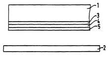
- the figure shows the layer sequence of the metals before soldering.
- an aluminum layer 3 is applied to the semiconductor body 1, which adheres well to silicon and in particular forms a perfect ohmic contact with p-doped silicon.
- a diffusion barrier layer 4 which is made of chromium or titanium and has a thickness of approximately 50 nm, sits on the aluminum layer 3. This layer is either sputtered directly onto the aluminum layer 3 or vapor-deposited directly.
- An adhesion promoter layer, for example Cu (not shown) is applied to the diffusion barrier layer 4 or the solder material is applied directly.
- the solder layer is made of either tin, gallium or lead and has a thickness of 1000 to 3000 nm, typically a thickness of approximately 2700 nm when using tin.
- the silicon semiconductor body 1 metallized in this way is then pressed onto the metal carrier plate 2, which usually consists of copper, and is connected to it at approximately 300 ° C. under a protective gas atmosphere or under vacuum conditions, whereby a metallurgical connection between diffusion barrier layer 4, solder material layer 5 and carrier plate 2 is formed, which is stable up to a temperature of approx. 450 ° C.
- the method according to the invention When using the method according to the invention, a product of high quality is produced, since the layer sequence described results in particularly good mechanically and electrically stable contact.
- the method can be described as very advantageous compared to the prior art from both a technological, economic and ecological point of view.
- the method according to the invention opens up the possibility of further reducing the thicknesses of the silicon semiconductor substrates, which leads to an improvement in the transmission properties of power semiconductor components.
- the economic advantages are that the material costs can be reduced and the throughput in production can be increased.
- the ecological advantage of the process according to the invention is that soldering is carried out without flux, so that cleaning steps with CFC-containing solvents can be avoided.
Landscapes
- Die Bonding (AREA)
- Internal Circuitry In Semiconductor Integrated Circuit Devices (AREA)
- Electrodes Of Semiconductors (AREA)
Applications Claiming Priority (2)
| Application Number | Priority Date | Filing Date | Title |
|---|---|---|---|
| DE19606101A DE19606101A1 (de) | 1996-02-19 | 1996-02-19 | Halbleiterkörper mit Lotmaterialschicht |
| DE19606101 | 1996-02-19 |
Publications (3)
| Publication Number | Publication Date |
|---|---|
| EP0790647A2 true EP0790647A2 (fr) | 1997-08-20 |
| EP0790647A3 EP0790647A3 (fr) | 1999-06-02 |
| EP0790647B1 EP0790647B1 (fr) | 2004-04-21 |
Family
ID=7785797
Family Applications (1)
| Application Number | Title | Priority Date | Filing Date |
|---|---|---|---|
| EP97102700A Expired - Lifetime EP0790647B1 (fr) | 1996-02-19 | 1997-02-19 | Corps semi-conducteur ayant une couche de soudure et procédé de soudage du corps semi-conducteur sur une plaque métallique de support |
Country Status (10)
| Country | Link |
|---|---|
| US (1) | US5901901A (fr) |
| EP (1) | EP0790647B1 (fr) |
| JP (1) | JP2983486B2 (fr) |
| KR (1) | KR100454755B1 (fr) |
| CN (1) | CN1126171C (fr) |
| AT (1) | ATE265090T1 (fr) |
| DE (2) | DE19606101A1 (fr) |
| MY (1) | MY124335A (fr) |
| SG (1) | SG69995A1 (fr) |
| TW (1) | TW437028B (fr) |
Cited By (5)
| Publication number | Priority date | Publication date | Assignee | Title |
|---|---|---|---|---|
| EP0833384A3 (fr) * | 1996-09-25 | 1999-10-13 | Siemens Aktiengesellschaft | Corps semi-conducteur comprenant une couche de brasure |
| US8461645B2 (en) | 2011-03-16 | 2013-06-11 | Infineon Technologies Austria Ag | Power semiconductor device |
| US8587116B2 (en) | 2010-09-30 | 2013-11-19 | Infineon Technologies Ag | Semiconductor module comprising an insert |
| US9082878B2 (en) | 2010-09-09 | 2015-07-14 | Infineon Technologies Ag | Method of fabricating a power semiconductor chip package |
| US9214442B2 (en) | 2007-03-19 | 2015-12-15 | Infineon Technologies Ag | Power semiconductor module, method for producing a power semiconductor module, and semiconductor chip |
Families Citing this family (26)
| Publication number | Priority date | Publication date | Assignee | Title |
|---|---|---|---|---|
| USD351593S (en) | 1992-09-10 | 1994-10-18 | Matsushita Electric Industrial Co., Ltd. | Optical disk cartridge |
| US6118351A (en) * | 1997-06-10 | 2000-09-12 | Lucent Technologies Inc. | Micromagnetic device for power processing applications and method of manufacture therefor |
| US6440750B1 (en) | 1997-06-10 | 2002-08-27 | Agere Systems Guardian Corporation | Method of making integrated circuit having a micromagnetic device |
| DE19735760A1 (de) * | 1997-08-18 | 1999-02-25 | Zeiss Carl Fa | Lötverfahren für optische Materialien an Metallfassungen und gefaßte Baugruppen |
| DE19740904B4 (de) | 1997-09-17 | 2004-10-28 | Infineon Technologies Ag | Verfahren zum Beseitigen von Sauerstoff-Restverunreinigungen aus tiegelgezogenen Siliziumwafern |
| US6255714B1 (en) | 1999-06-22 | 2001-07-03 | Agere Systems Guardian Corporation | Integrated circuit having a micromagnetic device including a ferromagnetic core and method of manufacture therefor |
| KR100594565B1 (ko) * | 1999-08-04 | 2006-06-28 | 삼성전자주식회사 | 액정표시장치 |
| DE19951945A1 (de) * | 1999-10-28 | 2001-05-03 | Daimler Chrysler Ag | Halbleiterbauelement mit Seitenwandmetallisierung |
| JP4544675B2 (ja) * | 1999-12-21 | 2010-09-15 | ローム株式会社 | 半導体装置の製造方法 |
| EP1320889A1 (fr) * | 2000-09-29 | 2003-06-25 | Infineon Technologies AG | Dispositif de connexion |
| DE10124141B4 (de) * | 2000-09-29 | 2009-11-26 | Infineon Technologies Ag | Verbindungseinrichtung für eine elektronische Schaltungsanordnung und Schaltungsanordnung |
| DE10103294C1 (de) * | 2001-01-25 | 2002-10-31 | Siemens Ag | Träger mit einer Metallfläche und mindestens ein darauf angeordneter Chip, insbesondere Leistungshalbleiter |
| DE102004001956B4 (de) | 2004-01-13 | 2007-02-01 | Infineon Technologies Ag | Umverdrahtungssubstratstreifen mit mehreren Halbleiterbauteilpositionen |
| US7347354B2 (en) * | 2004-03-23 | 2008-03-25 | Intel Corporation | Metallic solder thermal interface material layer and application of the same |
| US7868472B2 (en) * | 2004-04-08 | 2011-01-11 | Avago Technologies General Ip (Singapore) Pte. Ltd. | Thermal dissipation in integrated circuit systems |
| JP4882229B2 (ja) * | 2004-09-08 | 2012-02-22 | 株式会社デンソー | 半導体装置およびその製造方法 |
| DE102005031836B4 (de) | 2005-07-06 | 2007-11-22 | Infineon Technologies Ag | Halbleiterleistungsmodul mit SiC-Leistungsdioden und Verfahren zur Herstellung desselben |
| EP1748480B1 (fr) | 2005-07-28 | 2009-06-24 | Infineon Technologies AG | Structure de connexion pour fixer une puce semi-conductrice à un substrat métallique, puce semi-conductrice et composant électronique ayant cette structure de connexion et méthodes de fabrication de cette structure de connexion |
| DE102005052563B4 (de) | 2005-11-02 | 2016-01-14 | Infineon Technologies Ag | Halbleiterchip, Halbleiterbauteil und Verfahren zu deren Herstellung |
| US7508012B2 (en) | 2006-01-18 | 2009-03-24 | Infineon Technologies Ag | Electronic component and method for its assembly |
| US8951478B2 (en) * | 2006-03-30 | 2015-02-10 | Applied Materials, Inc. | Ampoule with a thermally conductive coating |
| DE102006031405B4 (de) * | 2006-07-05 | 2019-10-17 | Infineon Technologies Ag | Halbleitermodul mit Schaltfunktionen und Verfahren zur Herstellung desselben |
| DE102006048448A1 (de) * | 2006-10-11 | 2008-04-17 | Endress + Hauser Wetzer Gmbh + Co. Kg | Erzeugen einer Lotverbindung |
| CN101950737A (zh) * | 2009-11-23 | 2011-01-19 | 杭州士兰集成电路有限公司 | P型硅衬底背面金属化的制作方法 |
| DE102016226103B3 (de) | 2016-12-22 | 2018-05-09 | Conti Temic Microelectronic Gmbh | Verfahren zur Herstellung einer elektrischen Verbindung und elektrische Verbindung zwischen zwei Komponenten |
| US10910508B1 (en) * | 2018-05-04 | 2021-02-02 | National Technology & Engineering Solutions Of Sandia, Llc | Method of fabricating photosensitive devices with reduced process-temperature budget |
Family Cites Families (15)
| Publication number | Priority date | Publication date | Assignee | Title |
|---|---|---|---|---|
| US2474039A (en) * | 1945-03-03 | 1949-06-21 | Metals & Controls Corp | Method of forming composite metal having a nickel-plated beryllium-copper base and gold or silver bonded thereto by a copper-plated iron sheet |
| GB1149606A (en) * | 1967-02-27 | 1969-04-23 | Motorola Inc | Mounting for a semiconductor wafer which is resistant to fatigue caused by thermal stresses |
| DE2522773A1 (de) * | 1973-08-09 | 1976-12-02 | Siemens Ag | Weichgeloetete kontaktanordnung |
| US4451972A (en) * | 1980-01-21 | 1984-06-05 | National Semiconductor Corporation | Method of making electronic chip with metalized back including a surface stratum of solder |
| DE3406542A1 (de) * | 1984-02-23 | 1985-08-29 | Telefunken electronic GmbH, 7100 Heilbronn | Verfahren zum herstellen eines halbleiterbauelementes |
| JPS63238994A (ja) * | 1987-03-25 | 1988-10-05 | Tdk Corp | 半田組成物 |
| DE3740773A1 (de) * | 1987-12-02 | 1989-06-15 | Philips Patentverwaltung | Verfahren zum herstellen elektrisch leitender verbindungen |
| DE3823347A1 (de) * | 1988-07-09 | 1990-01-11 | Semikron Elektronik Gmbh | Leistungs-halbleiterelement |
| DE69021438T2 (de) * | 1989-05-16 | 1996-01-25 | Marconi Gec Ltd | Verfahren zur Herstellung einer Flip-Chip-Lötstruktur für Anordnungen mit Gold-Metallisierung. |
| US5027189A (en) * | 1990-01-10 | 1991-06-25 | Hughes Aircraft Company | Integrated circuit solder die-attach design and method |
| DE9212486U1 (de) * | 1992-09-16 | 1993-03-04 | Siemens AG, 8000 München | Halbleiterkörper mit verlöteter Trägerplatte |
| DE69325065T2 (de) * | 1992-10-02 | 1999-10-28 | Matsushita Electric Industrial Co., Ltd. | Halbleitervorrichtung, Bildabtastvorrichtung und Verfahren zu ihrer Herstellung |
| DE4241439A1 (de) * | 1992-12-10 | 1994-06-16 | Daimler Benz Ag | Verfahren zur Erzeugung einer formschlüssigen Verbindung zwischen metallischen Verbindern und metallischen Kontakten von Halbleiteroberflächen |
| US5816478A (en) * | 1995-06-05 | 1998-10-06 | Motorola, Inc. | Fluxless flip-chip bond and a method for making |
| US5803343A (en) * | 1995-10-30 | 1998-09-08 | Delco Electronics Corp. | Solder process for enhancing reliability of multilayer hybrid circuits |
-
1996
- 1996-02-19 DE DE19606101A patent/DE19606101A1/de not_active Withdrawn
-
1997
- 1997-02-14 SG SG1997000324A patent/SG69995A1/en unknown
- 1997-02-14 JP JP9047059A patent/JP2983486B2/ja not_active Expired - Fee Related
- 1997-02-17 TW TW086101824A patent/TW437028B/zh not_active IP Right Cessation
- 1997-02-18 MY MYPI97000591A patent/MY124335A/en unknown
- 1997-02-19 AT AT97102700T patent/ATE265090T1/de not_active IP Right Cessation
- 1997-02-19 KR KR1019970004939A patent/KR100454755B1/ko not_active Expired - Fee Related
- 1997-02-19 CN CN97104969A patent/CN1126171C/zh not_active Expired - Lifetime
- 1997-02-19 US US08/802,134 patent/US5901901A/en not_active Expired - Lifetime
- 1997-02-19 DE DE59711523T patent/DE59711523D1/de not_active Expired - Lifetime
- 1997-02-19 EP EP97102700A patent/EP0790647B1/fr not_active Expired - Lifetime
Cited By (6)
| Publication number | Priority date | Publication date | Assignee | Title |
|---|---|---|---|---|
| EP0833384A3 (fr) * | 1996-09-25 | 1999-10-13 | Siemens Aktiengesellschaft | Corps semi-conducteur comprenant une couche de brasure |
| US6268659B1 (en) | 1996-09-25 | 2001-07-31 | Infineon Technologies Ag | Semiconductor body with layer of solder material comprising chromium |
| US9214442B2 (en) | 2007-03-19 | 2015-12-15 | Infineon Technologies Ag | Power semiconductor module, method for producing a power semiconductor module, and semiconductor chip |
| US9082878B2 (en) | 2010-09-09 | 2015-07-14 | Infineon Technologies Ag | Method of fabricating a power semiconductor chip package |
| US8587116B2 (en) | 2010-09-30 | 2013-11-19 | Infineon Technologies Ag | Semiconductor module comprising an insert |
| US8461645B2 (en) | 2011-03-16 | 2013-06-11 | Infineon Technologies Austria Ag | Power semiconductor device |
Also Published As
| Publication number | Publication date |
|---|---|
| TW437028B (en) | 2001-05-28 |
| CN1168536A (zh) | 1997-12-24 |
| JPH1012507A (ja) | 1998-01-16 |
| DE59711523D1 (de) | 2004-05-27 |
| MY124335A (en) | 2006-06-30 |
| EP0790647A3 (fr) | 1999-06-02 |
| CN1126171C (zh) | 2003-10-29 |
| EP0790647B1 (fr) | 2004-04-21 |
| KR100454755B1 (ko) | 2005-01-13 |
| KR970063589A (ko) | 1997-09-12 |
| DE19606101A1 (de) | 1997-08-21 |
| ATE265090T1 (de) | 2004-05-15 |
| JP2983486B2 (ja) | 1999-11-29 |
| US5901901A (en) | 1999-05-11 |
| SG69995A1 (en) | 2000-01-25 |
Similar Documents
| Publication | Publication Date | Title |
|---|---|---|
| EP0790647B1 (fr) | Corps semi-conducteur ayant une couche de soudure et procédé de soudage du corps semi-conducteur sur une plaque métallique de support | |
| EP0049007B1 (fr) | Procédé pour la liaison directe de feuilles en cuivre à substrats en céramique d'oxydes | |
| DE69834771T2 (de) | Verbundkörper aus Keramik und Verfahren zu seiner Herstellung | |
| EP0950261B1 (fr) | Semiconducteur avec metallisation de la face arriere | |
| DE69621222T2 (de) | Keramische leiterplatte | |
| DE69321904T2 (de) | Verfahren für eine permanente metallische Verbindung | |
| DE69318975T2 (de) | Verfahren zur verbindung einer sputter-targetträgerplatteneinheit | |
| DE69217617T2 (de) | Verbindungsverfahren unter Verwendung eines aus mehrfach abwechselnden Gold- und Zinnschichten bestehenden Lotes | |
| DE69410548T2 (de) | Wolfram Metallisierung des CVD-Diamantes | |
| DE60214572T2 (de) | Hartlötbare metallisierungen für diamantbauteile | |
| DE69812533T2 (de) | Aluminiumnitridsubstrat und Verfahren zu dessen Herstellung | |
| US3413711A (en) | Method of making palladium copper contact for soldering | |
| DE3851819T2 (de) | Hoch-TC-Supraleitende Einheiten mit geringem Oberflächenwiderstand. | |
| DE3107943A1 (de) | Verfahren zur herstellung von loetbaren und temperfaehigen edelmetallfreien duennschichtleiterbahnen | |
| DE69219529T2 (de) | Verfahren zum Aufbringen einer Metall- oder Passivierenschicht mit hoher Haftung über einem isolierten Halbleitersubstrat | |
| DE112012006812T5 (de) | Elektronische Komponente und Fertigungsverfahren für elektronische Komponente | |
| DE19639438A1 (de) | Halbleiterkörper mit Lotmaterialschicht | |
| DE19603654C1 (de) | Verfahren zum Löten eines Halbleiterkörpers auf eine Trägerplatte und Halbleiterkörper zur Durchführung des Verfahrens | |
| DE3830131C2 (fr) | ||
| DE1816748A1 (de) | Halbleitervorrichtung und Verfahren zu ihrer Herstellung | |
| DE19954319C1 (de) | Verfahren zum Herstellen von mehrschichtigen Kontaktelektroden für Verbindungshalbeiter und Anordnung | |
| DE3040493C2 (de) | Verfahren zum lötflußmittelfreien Anlöten einer Glasfläche an eine Metallfläche | |
| DE2207012C2 (de) | Verfahren zur Kontaktierung von Halbleiterbauelementen | |
| DE7106898U (de) | Integrierter Hybrid Schaltkreis | |
| DE3227898A1 (de) | Schichtsystem fuer optoelektronische anzeigen |
Legal Events
| Date | Code | Title | Description |
|---|---|---|---|
| PUAI | Public reference made under article 153(3) epc to a published international application that has entered the european phase |
Free format text: ORIGINAL CODE: 0009012 |
|
| AK | Designated contracting states |
Kind code of ref document: A2 Designated state(s): AT DE FR GB IE NL |
|
| PUAL | Search report despatched |
Free format text: ORIGINAL CODE: 0009013 |
|
| AK | Designated contracting states |
Kind code of ref document: A3 Designated state(s): AT DE FR GB IE NL |
|
| 17P | Request for examination filed |
Effective date: 19990903 |
|
| RAP1 | Party data changed (applicant data changed or rights of an application transferred) |
Owner name: INFINEON TECHNOLOGIES AG |
|
| 17Q | First examination report despatched |
Effective date: 20020703 |
|
| GRAP | Despatch of communication of intention to grant a patent |
Free format text: ORIGINAL CODE: EPIDOSNIGR1 |
|
| GRAS | Grant fee paid |
Free format text: ORIGINAL CODE: EPIDOSNIGR3 |
|
| GRAA | (expected) grant |
Free format text: ORIGINAL CODE: 0009210 |
|
| AK | Designated contracting states |
Kind code of ref document: B1 Designated state(s): AT DE FR GB IE NL |
|
| PG25 | Lapsed in a contracting state [announced via postgrant information from national office to epo] |
Ref country code: NL Free format text: LAPSE BECAUSE OF FAILURE TO SUBMIT A TRANSLATION OF THE DESCRIPTION OR TO PAY THE FEE WITHIN THE PRESCRIBED TIME-LIMIT Effective date: 20040421 |
|
| REG | Reference to a national code |
Ref country code: GB Ref legal event code: FG4D Free format text: NOT ENGLISH |
|
| REG | Reference to a national code |
Ref country code: IE Ref legal event code: FG4D Free format text: GERMAN |
|
| REF | Corresponds to: |
Ref document number: 59711523 Country of ref document: DE Date of ref document: 20040527 Kind code of ref document: P |
|
| GBT | Gb: translation of ep patent filed (gb section 77(6)(a)/1977) |
Effective date: 20040622 |
|
| NLV1 | Nl: lapsed or annulled due to failure to fulfill the requirements of art. 29p and 29m of the patents act | ||
| ET | Fr: translation filed | ||
| PLBE | No opposition filed within time limit |
Free format text: ORIGINAL CODE: 0009261 |
|
| STAA | Information on the status of an ep patent application or granted ep patent |
Free format text: STATUS: NO OPPOSITION FILED WITHIN TIME LIMIT |
|
| 26N | No opposition filed |
Effective date: 20050124 |
|
| NLXE | Nl: other communications concerning ep-patents (part 3 heading xe) |
Free format text: HEADING VE, SECTION 1, ISSUED 20041001; PATENTNUMBER 0790647 SHOULD BE DELETED. |
|
| PGFP | Annual fee paid to national office [announced via postgrant information from national office to epo] |
Ref country code: NL Payment date: 20070213 Year of fee payment: 11 Ref country code: AT Payment date: 20070213 Year of fee payment: 11 |
|
| PGFP | Annual fee paid to national office [announced via postgrant information from national office to epo] |
Ref country code: GB Payment date: 20070216 Year of fee payment: 11 |
|
| PGFP | Annual fee paid to national office [announced via postgrant information from national office to epo] |
Ref country code: IE Payment date: 20070220 Year of fee payment: 11 |
|
| GBPC | Gb: european patent ceased through non-payment of renewal fee |
Effective date: 20080219 |
|
| NLV4 | Nl: lapsed or anulled due to non-payment of the annual fee |
Effective date: 20080901 |
|
| REG | Reference to a national code |
Ref country code: IE Ref legal event code: MM4A |
|
| PG25 | Lapsed in a contracting state [announced via postgrant information from national office to epo] |
Ref country code: AT Free format text: LAPSE BECAUSE OF NON-PAYMENT OF DUE FEES Effective date: 20080219 |
|
| PG25 | Lapsed in a contracting state [announced via postgrant information from national office to epo] |
Ref country code: IE Free format text: LAPSE BECAUSE OF NON-PAYMENT OF DUE FEES Effective date: 20080219 |
|
| PG25 | Lapsed in a contracting state [announced via postgrant information from national office to epo] |
Ref country code: GB Free format text: LAPSE BECAUSE OF NON-PAYMENT OF DUE FEES Effective date: 20080219 |
|
| REG | Reference to a national code |
Ref country code: FR Ref legal event code: PLFP Year of fee payment: 20 |
|
| PGFP | Annual fee paid to national office [announced via postgrant information from national office to epo] |
Ref country code: FR Payment date: 20160218 Year of fee payment: 20 |
|
| PGFP | Annual fee paid to national office [announced via postgrant information from national office to epo] |
Ref country code: DE Payment date: 20160419 Year of fee payment: 20 |
|
| REG | Reference to a national code |
Ref country code: DE Ref legal event code: R071 Ref document number: 59711523 Country of ref document: DE |