EP0790761A1 - Elément de contact pour une mise immédiate à la masse - Google Patents
Elément de contact pour une mise immédiate à la masse Download PDFInfo
- Publication number
- EP0790761A1 EP0790761A1 EP97101156A EP97101156A EP0790761A1 EP 0790761 A1 EP0790761 A1 EP 0790761A1 EP 97101156 A EP97101156 A EP 97101156A EP 97101156 A EP97101156 A EP 97101156A EP 0790761 A1 EP0790761 A1 EP 0790761A1
- Authority
- EP
- European Patent Office
- Prior art keywords
- contact element
- element according
- plug
- contact
- area
- Prior art date
- Legal status (The legal status is an assumption and is not a legal conclusion. Google has not performed a legal analysis and makes no representation as to the accuracy of the status listed.)
- Granted
Links
- 208000010201 Exanthema Diseases 0.000 title 1
- 201000005884 exanthem Diseases 0.000 title 1
- 206010037844 rash Diseases 0.000 title 1
- 238000000034 method Methods 0.000 claims abstract description 4
- 239000004020 conductor Substances 0.000 claims description 5
- RYGMFSIKBFXOCR-UHFFFAOYSA-N Copper Chemical compound [Cu] RYGMFSIKBFXOCR-UHFFFAOYSA-N 0.000 claims description 2
- 238000005452 bending Methods 0.000 claims description 2
- 229910052802 copper Inorganic materials 0.000 claims description 2
- 239000010949 copper Substances 0.000 claims description 2
- 230000001681 protective effect Effects 0.000 abstract description 9
- 238000003780 insertion Methods 0.000 abstract description 5
- 230000037431 insertion Effects 0.000 abstract description 5
- 230000000454 anti-cipatory effect Effects 0.000 abstract 1
- 238000001125 extrusion Methods 0.000 abstract 1
- 230000000295 complement effect Effects 0.000 description 2
- 230000000694 effects Effects 0.000 description 2
- 238000004519 manufacturing process Methods 0.000 description 2
- 230000000284 resting effect Effects 0.000 description 2
- 239000000956 alloy Substances 0.000 description 1
- 229910045601 alloy Inorganic materials 0.000 description 1
- 230000002146 bilateral effect Effects 0.000 description 1
- 239000002184 metal Substances 0.000 description 1
- 229910052751 metal Inorganic materials 0.000 description 1
- 230000002028 premature Effects 0.000 description 1
Images
Classifications
-
- H—ELECTRICITY
- H01—ELECTRIC ELEMENTS
- H01R—ELECTRICALLY-CONDUCTIVE CONNECTIONS; STRUCTURAL ASSOCIATIONS OF A PLURALITY OF MUTUALLY-INSULATED ELECTRICAL CONNECTING ELEMENTS; COUPLING DEVICES; CURRENT COLLECTORS
- H01R13/00—Details of coupling devices of the kinds covered by groups H01R12/70 or H01R24/00 - H01R33/00
- H01R13/02—Contact members
- H01R13/10—Sockets for co-operation with pins or blades
- H01R13/11—Resilient sockets
- H01R13/112—Resilient sockets forked sockets having two legs
-
- H—ELECTRICITY
- H01—ELECTRIC ELEMENTS
- H01R—ELECTRICALLY-CONDUCTIVE CONNECTIONS; STRUCTURAL ASSOCIATIONS OF A PLURALITY OF MUTUALLY-INSULATED ELECTRICAL CONNECTING ELEMENTS; COUPLING DEVICES; CURRENT COLLECTORS
- H01R13/00—Details of coupling devices of the kinds covered by groups H01R12/70 or H01R24/00 - H01R33/00
- H01R13/648—Protective earth or shield arrangements on coupling devices, e.g. anti-static shielding
- H01R13/658—High frequency shielding arrangements, e.g. against EMI [Electro-Magnetic Interference] or EMP [Electro-Magnetic Pulse]
- H01R13/6591—Specific features or arrangements of connection of shield to conductive members
- H01R13/6597—Specific features or arrangements of connection of shield to conductive members the conductive member being a contact of the connector
-
- H—ELECTRICITY
- H01—ELECTRIC ELEMENTS
- H01R—ELECTRICALLY-CONDUCTIVE CONNECTIONS; STRUCTURAL ASSOCIATIONS OF A PLURALITY OF MUTUALLY-INSULATED ELECTRICAL CONNECTING ELEMENTS; COUPLING DEVICES; CURRENT COLLECTORS
- H01R4/00—Electrically-conductive connections between two or more conductive members in direct contact, i.e. touching one another; Means for effecting or maintaining such contact; Electrically-conductive connections having two or more spaced connecting locations for conductors and using contact members penetrating insulation
- H01R4/58—Electrically-conductive connections between two or more conductive members in direct contact, i.e. touching one another; Means for effecting or maintaining such contact; Electrically-conductive connections having two or more spaced connecting locations for conductors and using contact members penetrating insulation characterised by the form or material of the contacting members
- H01R4/64—Connections between or with conductive parts having primarily a non-electric function, e.g. frame, casing, rail
-
- H—ELECTRICITY
- H05—ELECTRIC TECHNIQUES NOT OTHERWISE PROVIDED FOR
- H05K—PRINTED CIRCUITS; CASINGS OR CONSTRUCTIONAL DETAILS OF ELECTRIC APPARATUS; MANUFACTURE OF ASSEMBLAGES OF ELECTRICAL COMPONENTS
- H05K7/00—Constructional details common to different types of electric apparatus
- H05K7/14—Mounting supporting structure in casing or on frame or rack
- H05K7/1401—Mounting supporting structure in casing or on frame or rack comprising clamping or extracting means
- H05K7/1402—Mounting supporting structure in casing or on frame or rack comprising clamping or extracting means for securing or extracting printed circuit boards
- H05K7/1409—Mounting supporting structure in casing or on frame or rack comprising clamping or extracting means for securing or extracting printed circuit boards by lever-type mechanisms
-
- H—ELECTRICITY
- H05—ELECTRIC TECHNIQUES NOT OTHERWISE PROVIDED FOR
- H05K—PRINTED CIRCUITS; CASINGS OR CONSTRUCTIONAL DETAILS OF ELECTRIC APPARATUS; MANUFACTURE OF ASSEMBLAGES OF ELECTRICAL COMPONENTS
- H05K9/00—Screening of apparatus or components against electric or magnetic fields
- H05K9/0007—Casings
- H05K9/0015—Gaskets or seals
- H05K9/0016—Gaskets or seals having a spring contact
Definitions
- the invention relates to a contact element for leading grounding of a plug-in module, for example a printed circuit board, a plug-in board, a plug-in block or a cassette, during insertion into guide rails of a housing or a subrack until the plug-in process.
- a plug-in module for example a printed circuit board, a plug-in board, a plug-in block or a cassette
- grounding is also required when plugging in a plug-in module that is contacted with a voltage of 50 V.
- a known protective conductor connection provides for the use of a contact spring in the area of a conductive guide rail of a subrack.
- the contact spring is inserted into the guide rail, which is usually made of plastic, and creates an electrical connection when a plug-in module is inserted.
- a disadvantage of this design is that the contact spring is arranged within the guide rail and does not always guarantee the required leading protective ground when inserted.
- the invention has for its object to provide an inexpensive to manufacture and assemble contact element, which ensures safe and effective protective grounding and a very early dissipation of electrostatic charges when plugging in plug-in modules.
- a contact element with a clamping area and with a holding area is used for the premature grounding of plug connectors, the holding area resting on or resting on a transverse profile of the housing or subrack and in particular being held thereon.
- An outer edge of the cross section is covered by the holding area and extremely early protective earthing and discharge of electrostatic charges is achieved.
- the clamping area is designed in such a way that a printed circuit board or a side edge of a plug-in block or a cassette is received and guided, wherein in particular a bilateral contact with a printed circuit board or on a side edge of a plug-in block or a cassette is ensured.
- the clamping region is expediently formed by two spring-like contact strips which run parallel to one another and expediently have a distance which corresponds to the thickness of a printed circuit board or a side edge.
- a particularly effective electrical connection is achieved with clamping arches, which are formed on the contact strips in particular at the ends and are directed toward one another.
- the horizontally aligned contact strips of the clamping area and the holding area are arranged in the installed state essentially in the area of the transverse profile of the housing and in front of a guide rail, the clamping arc area of the contact strips being able to run above the guide rail.
- the holding area has at least one front cross piece, which is preferably complementary to a groove in the cross section of the housing or subrack.
- a further, for example rear, cross piece is advantageous, which can also cooperate with a groove of the cross section.
- the holding area is essentially horizontal and is designed as a flat contact surface which rests on a complementary profile area of the cross section. In the area of an upper outer edge of the transverse profile, when the contact element is installed, there is an elevation of the holding area, which can be designed in particular in an arc shape. This part of the holding area serves to support a plug-in and pull-out aid and improves its leverage and thus the insertion and removal of printed circuit boards and other plug-in modules.
- the contact element which is designed as an expanded Z in a side view, has connecting webs which are arranged almost vertically and have a U-shaped receptacle for a printed circuit board or between the holding area arranged as the lower transverse bar and the spring-like contact strips which represent the upper transverse bar forms a side edge of a plug-in module. A region of a plug-in and removal aid can also be moved into this receptacle during its actuation.
- the clamping arches which are arranged at the ends of the contact strips facing the housing interior, have a particularly advantageous effect. Since the contact element according to the invention extends to or over an outer edge of the transverse profile of the housing or subrack, effective and early leading grounding is ensured. When pulling plug-in modules, the electrical connection of the leading contact element is the last to be interrupted. In addition, early dissipation of electrostatic charges from printed circuit boards, plug-in modules and their front plates is guaranteed.
- the design of the one-piece contact element enables cost-effective production and assembly.
- the contact element can be produced by a stamping and bending process.
- the contact element is expediently made of a conductive material with good spring action, e.g. made of copper or a corresponding alloy.
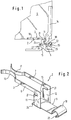
- a contact element 2 for early grounding of a connector of a circuit board 9 is shown.
- the contact element 2 is held on a lower cross section 15 of a subrack (not shown) and extends with a holding area 5 and an arch-shaped elevation or a support arch 18 formed at its free end to an outer edge or to the front area 20 of the cross section 15.
- the arcuate elevation or the support arch 18 with an approximately semicircular cross section serves as a support point for a plug-in and removal aid 14 when inserting the circuit board 9 into a clamping area 3 of the contact element 2 and then into a guide rail (not shown), with a male connector of the circuit board and a female connector of the subrack (not shown) can be connected.
- FIG. 1 shows the fixation of the contact element 2 on the transverse profile 15 of a housing or subrack with transverse webs 22, 24 formed on the holding area 5, which cooperate with complementarily designed grooves 25, 27 of the transverse profile 15.
- the design and arrangement of a front cross piece 22 and a rear cross piece 24 can also be seen in FIG. 2.
- the holding area 5 has vertical connecting webs 11, 12 at an area directed towards the interior of the housing (not shown).
- the connecting webs 11, 12 and the holding area 5 in the area of the connecting webs 11, 12 form a U-shaped receiving opening 13 which, for example, during the insertion and during the pulling of a printed circuit board 9, receive an area of a plug-in and pull-out aid 14 (FIG. 1) can.
- a conductive connection between the circuit board 9 and the contact element 2 is, as FIG. 1 clearly shows, realized by the clamping area 3.
- the clamping area 3 has two contact strips 6, 7 for contacting both side surfaces of the printed circuit board 9. With arcuate areas or clamping arches 16, 17 formed at the ends, which are directed towards each other, a clamping guide of the printed circuit board 9 is achieved during insertion and removal and a particularly secure protective grounding.
- the distance between the contact strips 6, 7 and the resiliently expandable clamping arches 16, 17 corresponds to the dimensions of a printed circuit board or a side edge of a cassette or a plug-in block.
- Recesses 21 have an advantageous effect in the connection area between the connecting webs 11, 12 and the contact strips 6, 7.
- the recesses 21 improve the spring action in the horizontal and vertical directions.
Landscapes
- Engineering & Computer Science (AREA)
- Microelectronics & Electronic Packaging (AREA)
- Coupling Device And Connection With Printed Circuit (AREA)
- Mounting Of Printed Circuit Boards And The Like (AREA)
- Details Of Connecting Devices For Male And Female Coupling (AREA)
- Multi-Conductor Connections (AREA)
- Elimination Of Static Electricity (AREA)
- Waveguide Aerials (AREA)
- Non-Reversible Transmitting Devices (AREA)
- Control Of Motors That Do Not Use Commutators (AREA)
Applications Claiming Priority (2)
| Application Number | Priority Date | Filing Date | Title |
|---|---|---|---|
| DE29602428U | 1996-02-12 | ||
| DE29602428U DE29602428U1 (de) | 1996-02-12 | 1996-02-12 | Kontaktelement zur voreilenden Erdung |
Publications (2)
| Publication Number | Publication Date |
|---|---|
| EP0790761A1 true EP0790761A1 (fr) | 1997-08-20 |
| EP0790761B1 EP0790761B1 (fr) | 1999-07-21 |
Family
ID=8019359
Family Applications (1)
| Application Number | Title | Priority Date | Filing Date |
|---|---|---|---|
| EP97101156A Expired - Lifetime EP0790761B1 (fr) | 1996-02-12 | 1997-01-24 | Assemblage pour une mise immédiate à la masse |
Country Status (6)
| Country | Link |
|---|---|
| US (1) | US5879167A (fr) |
| EP (1) | EP0790761B1 (fr) |
| JP (1) | JP2791320B2 (fr) |
| CN (1) | CN1166702A (fr) |
| AT (1) | ATE182436T1 (fr) |
| DE (2) | DE29602428U1 (fr) |
Families Citing this family (7)
| Publication number | Priority date | Publication date | Assignee | Title |
|---|---|---|---|---|
| DE19644416C1 (de) * | 1996-10-25 | 1997-11-20 | Schroff Gmbh | Kontaktelement zur elektrischen Kontaktierung von Leiterkarten mit einer vorderen Modulschiene eines Baugruppenträgers |
| NL1015952C2 (nl) * | 2000-08-17 | 2002-02-19 | Ericsson Telefon Ab L M | Printkaartgeleider en werkwijze voor het vervaardigen daarvan. |
| JP3614768B2 (ja) * | 2000-10-20 | 2005-01-26 | タイコエレクトロニクスアンプ株式会社 | バッテリコネクタ |
| CN101969167B (zh) * | 2010-08-27 | 2013-01-23 | 深圳市普博科技有限公司 | 参数模块装入主机接口的方法及采用该方法的装置 |
| CN101998795A (zh) * | 2010-10-22 | 2011-03-30 | 南京深科博业电力自动化有限公司 | 接地结构 |
| CN108923150A (zh) * | 2018-06-28 | 2018-11-30 | 郑州云海信息技术有限公司 | 一种pwr连接器 |
| CN117387448A (zh) * | 2023-11-08 | 2024-01-12 | 浙江桦芯国创科技有限公司 | 一种电子雷管发火参数的检测系统及方法 |
Citations (6)
| Publication number | Priority date | Publication date | Assignee | Title |
|---|---|---|---|---|
| GB2142783A (en) * | 1983-06-29 | 1985-01-23 | Calabro Anthony Denis | Cage apparatus for printed circuit boards and method for preventing sharp spikes in the signal applied to said printed circuit boards |
| WO1987005776A1 (fr) * | 1986-03-21 | 1987-09-24 | Cgr Ultrasonic | Bac a cartes electroniques |
| EP0264686A1 (fr) * | 1986-10-09 | 1988-04-27 | Licentia Patent-Verwaltungs-GmbH | Barres de maintien connectables à des barres profilées d'un support de plaquettes de composants |
| DE9217302U1 (de) * | 1992-12-17 | 1993-02-25 | Siemens AG, 8000 München | Kunststoffträger zur Aufnahme und Halterung eines elektronischen Moduls |
| DE4141559A1 (de) * | 1991-12-17 | 1993-06-24 | Licentia Gmbh | Fuehrungshalter fuer elektronische baugruppen |
| US5533631A (en) * | 1994-10-12 | 1996-07-09 | Unitrack Industries, Inc. | Composite printed circuit card guide and holding device |
Family Cites Families (4)
| Publication number | Priority date | Publication date | Assignee | Title |
|---|---|---|---|---|
| DE8906491U1 (de) * | 1989-05-26 | 1989-07-20 | Rittal-Werk Rudolf Loh Gmbh & Co Kg, 6348 Herborn | Vorrichtung zum elektrisch leitenden Verbinden einer Leiterplatte mit einer Modulschiene eines Baugruppenträgers |
| JPH0793506B2 (ja) * | 1989-07-21 | 1995-10-09 | 北川工業株式会社 | 基板用ガイドレール |
| JP2504512Y2 (ja) * | 1991-07-18 | 1996-07-10 | 北川工業株式会社 | ガイドレ―ル |
| US5419708A (en) * | 1993-12-21 | 1995-05-30 | International Business Machines Corp. | Printed circuit card with minor surface I/O pads |
-
1996
- 1996-02-12 DE DE29602428U patent/DE29602428U1/de not_active Expired - Lifetime
-
1997
- 1997-01-24 EP EP97101156A patent/EP0790761B1/fr not_active Expired - Lifetime
- 1997-01-24 DE DE59700263T patent/DE59700263D1/de not_active Expired - Fee Related
- 1997-01-24 AT AT97101156T patent/ATE182436T1/de not_active IP Right Cessation
- 1997-02-10 JP JP9026949A patent/JP2791320B2/ja not_active Expired - Lifetime
- 1997-02-12 CN CN97102445A patent/CN1166702A/zh active Pending
- 1997-02-12 US US08/798,823 patent/US5879167A/en not_active Expired - Fee Related
Patent Citations (6)
| Publication number | Priority date | Publication date | Assignee | Title |
|---|---|---|---|---|
| GB2142783A (en) * | 1983-06-29 | 1985-01-23 | Calabro Anthony Denis | Cage apparatus for printed circuit boards and method for preventing sharp spikes in the signal applied to said printed circuit boards |
| WO1987005776A1 (fr) * | 1986-03-21 | 1987-09-24 | Cgr Ultrasonic | Bac a cartes electroniques |
| EP0264686A1 (fr) * | 1986-10-09 | 1988-04-27 | Licentia Patent-Verwaltungs-GmbH | Barres de maintien connectables à des barres profilées d'un support de plaquettes de composants |
| DE4141559A1 (de) * | 1991-12-17 | 1993-06-24 | Licentia Gmbh | Fuehrungshalter fuer elektronische baugruppen |
| DE9217302U1 (de) * | 1992-12-17 | 1993-02-25 | Siemens AG, 8000 München | Kunststoffträger zur Aufnahme und Halterung eines elektronischen Moduls |
| US5533631A (en) * | 1994-10-12 | 1996-07-09 | Unitrack Industries, Inc. | Composite printed circuit card guide and holding device |
Also Published As
| Publication number | Publication date |
|---|---|
| CN1166702A (zh) | 1997-12-03 |
| JP2791320B2 (ja) | 1998-08-27 |
| DE59700263D1 (de) | 1999-08-26 |
| ATE182436T1 (de) | 1999-08-15 |
| EP0790761B1 (fr) | 1999-07-21 |
| US5879167A (en) | 1999-03-09 |
| JPH09260877A (ja) | 1997-10-03 |
| DE29602428U1 (de) | 1996-03-28 |
Similar Documents
| Publication | Publication Date | Title |
|---|---|---|
| EP0898327B1 (fr) | Connecteur de carte de circuits | |
| DE69502830T2 (de) | Elektrischer verbinder mit führungsanordnung | |
| DE3886816T2 (de) | Elektrischer Steckverbinder. | |
| DE2409075A1 (de) | Elektrischer verbinder | |
| EP1758206A2 (fr) | Possibilité de connexion verticale dans une barette à bornes ayant des étages décalés | |
| DE102008033430B4 (de) | Verteileranschlussmodul für die Telekommunikations- und Datentechnik | |
| DE102018210233B4 (de) | Direktstecker und Direktsteckverbindung | |
| EP0735615A2 (fr) | Borne de jonction pour appareils électriques | |
| DE3322856A1 (de) | Frontsystem fuer in baugruppentraeger einschiebbare steckbaugruppen und rahmenartige baugruppentraeger zu deren aufnahme | |
| DE3436119C2 (de) | Kontaktfederelement zum Kontaktieren von Leiterplatten | |
| DE19644416C1 (de) | Kontaktelement zur elektrischen Kontaktierung von Leiterkarten mit einer vorderen Modulschiene eines Baugruppenträgers | |
| EP0790761B1 (fr) | Assemblage pour une mise immédiate à la masse | |
| DE20307174U1 (de) | Leuchtenanordnung | |
| DE3634462C2 (fr) | ||
| EP0126924A1 (fr) | Support pour des plaquettes de composants à fiches | |
| DE102022110373B4 (de) | Stromschienenverbinder und Stromschienensystem | |
| EP0937375A1 (fr) | Porte-cartes protege pour cartes a circuit imprime electriques | |
| DE3806049A1 (de) | Steckverbindung fuer elektrische leitungen | |
| EP1160921B1 (fr) | Connecteur pour connecter des fils à une carte à circuits | |
| DE2743194C2 (de) | Anordnung zum Anschließen von Leiterplatten in Baugruppenträgern an eine Potentialausgleichsleitung | |
| EP1414283A1 (fr) | Système de controle muni de moyens de suppression de signaux d'interférence | |
| EP0560261A1 (fr) | Dispositif pour le maintien de plaques de circuit dans un boîtier | |
| WO2007080069A1 (fr) | Appareil electrique | |
| DE9205780U1 (de) | Messerleiste für ein geschirmtes Übergabesystem | |
| EP4231459A1 (fr) | Dispositif de raccordement et unité de raccordement |
Legal Events
| Date | Code | Title | Description |
|---|---|---|---|
| PUAI | Public reference made under article 153(3) epc to a published international application that has entered the european phase |
Free format text: ORIGINAL CODE: 0009012 |
|
| AK | Designated contracting states |
Kind code of ref document: A1 Designated state(s): AT BE CH DE DK ES FI FR GB IT LI NL SE |
|
| 17P | Request for examination filed |
Effective date: 19970814 |
|
| 17Q | First examination report despatched |
Effective date: 19980227 |
|
| GRAG | Despatch of communication of intention to grant |
Free format text: ORIGINAL CODE: EPIDOS AGRA |
|
| GRAG | Despatch of communication of intention to grant |
Free format text: ORIGINAL CODE: EPIDOS AGRA |
|
| GRAH | Despatch of communication of intention to grant a patent |
Free format text: ORIGINAL CODE: EPIDOS IGRA |
|
| GRAH | Despatch of communication of intention to grant a patent |
Free format text: ORIGINAL CODE: EPIDOS IGRA |
|
| GRAA | (expected) grant |
Free format text: ORIGINAL CODE: 0009210 |
|
| AK | Designated contracting states |
Kind code of ref document: B1 Designated state(s): AT BE CH DE DK ES FI FR GB IT LI NL SE |
|
| PG25 | Lapsed in a contracting state [announced via postgrant information from national office to epo] |
Ref country code: SE Free format text: THE PATENT HAS BEEN ANNULLED BY A DECISION OF A NATIONAL AUTHORITY Effective date: 19990721 Ref country code: NL Free format text: LAPSE BECAUSE OF FAILURE TO SUBMIT A TRANSLATION OF THE DESCRIPTION OR TO PAY THE FEE WITHIN THE PRESCRIBED TIME-LIMIT Effective date: 19990721 Ref country code: IT Free format text: LAPSE BECAUSE OF FAILURE TO SUBMIT A TRANSLATION OF THE DESCRIPTION OR TO PAY THE FEE WITHIN THE PRE;WARNING: LAPSES OF ITALIAN PATENTS WITH EFFECTIVE DATE BEFORE 2007 MAY HAVE OCCURRED AT ANY TIME BEFORE 2007. THE CORRECT EFFECTIVE DATE MAY BE DIFFERENT FROM THE ONE RECORDED.SCRIBED TIME-LIMIT Effective date: 19990721 Ref country code: GB Free format text: LAPSE BECAUSE OF FAILURE TO SUBMIT A TRANSLATION OF THE DESCRIPTION OR TO PAY THE FEE WITHIN THE PRESCRIBED TIME-LIMIT Effective date: 19990721 Ref country code: FR Free format text: LAPSE BECAUSE OF FAILURE TO SUBMIT A TRANSLATION OF THE DESCRIPTION OR TO PAY THE FEE WITHIN THE PRESCRIBED TIME-LIMIT Effective date: 19990721 Ref country code: FI Free format text: LAPSE BECAUSE OF NON-PAYMENT OF DUE FEES Effective date: 19990721 Ref country code: ES Free format text: THE PATENT HAS BEEN ANNULLED BY A DECISION OF A NATIONAL AUTHORITY Effective date: 19990721 |
|
| REF | Corresponds to: |
Ref document number: 182436 Country of ref document: AT Date of ref document: 19990815 Kind code of ref document: T |
|
| REG | Reference to a national code |
Ref country code: CH Ref legal event code: EP |
|
| REF | Corresponds to: |
Ref document number: 59700263 Country of ref document: DE Date of ref document: 19990826 |
|
| PG25 | Lapsed in a contracting state [announced via postgrant information from national office to epo] |
Ref country code: DK Free format text: LAPSE BECAUSE OF FAILURE TO SUBMIT A TRANSLATION OF THE DESCRIPTION OR TO PAY THE FEE WITHIN THE PRESCRIBED TIME-LIMIT Effective date: 19991021 |
|
| EN | Fr: translation not filed | ||
| NLV1 | Nl: lapsed or annulled due to failure to fulfill the requirements of art. 29p and 29m of the patents act | ||
| GBV | Gb: ep patent (uk) treated as always having been void in accordance with gb section 77(7)/1977 [no translation filed] |
Effective date: 19990721 |
|
| PG25 | Lapsed in a contracting state [announced via postgrant information from national office to epo] |
Ref country code: AT Free format text: LAPSE BECAUSE OF NON-PAYMENT OF DUE FEES Effective date: 20000124 |
|
| PG25 | Lapsed in a contracting state [announced via postgrant information from national office to epo] |
Ref country code: BE Free format text: LAPSE BECAUSE OF NON-PAYMENT OF DUE FEES Effective date: 20000131 |
|
| PLBE | No opposition filed within time limit |
Free format text: ORIGINAL CODE: 0009261 |
|
| STAA | Information on the status of an ep patent application or granted ep patent |
Free format text: STATUS: NO OPPOSITION FILED WITHIN TIME LIMIT |
|
| 26N | No opposition filed | ||
| BERE | Be: lapsed |
Owner name: KNURR-MECHANIK FUR DIE ELEKTRONIK A.G. Effective date: 20000131 |
|
| PG25 | Lapsed in a contracting state [announced via postgrant information from national office to epo] |
Ref country code: LI Free format text: LAPSE BECAUSE OF NON-PAYMENT OF DUE FEES Effective date: 20010131 Ref country code: CH Free format text: LAPSE BECAUSE OF NON-PAYMENT OF DUE FEES Effective date: 20010131 |
|
| REG | Reference to a national code |
Ref country code: CH Ref legal event code: PL |
|
| PGFP | Annual fee paid to national office [announced via postgrant information from national office to epo] |
Ref country code: DE Payment date: 20030131 Year of fee payment: 7 |
|
| PG25 | Lapsed in a contracting state [announced via postgrant information from national office to epo] |
Ref country code: DE Free format text: LAPSE BECAUSE OF NON-PAYMENT OF DUE FEES Effective date: 20040803 |