EP0791929A2 - Dispositif électronique et méthode de sa duplication et système de transfert de données entre deux dispositifs électroniques similaires - Google Patents
Dispositif électronique et méthode de sa duplication et système de transfert de données entre deux dispositifs électroniques similaires Download PDFInfo
- Publication number
- EP0791929A2 EP0791929A2 EP96114934A EP96114934A EP0791929A2 EP 0791929 A2 EP0791929 A2 EP 0791929A2 EP 96114934 A EP96114934 A EP 96114934A EP 96114934 A EP96114934 A EP 96114934A EP 0791929 A2 EP0791929 A2 EP 0791929A2
- Authority
- EP
- European Patent Office
- Prior art keywords
- volatile memory
- interface
- microprocessor
- electronic device
- data
- Prior art date
- Legal status (The legal status is an assumption and is not a legal conclusion. Google has not performed a legal analysis and makes no representation as to the accuracy of the status listed.)
- Granted
Links
Images

Classifications
-
- G—PHYSICS
- G11—INFORMATION STORAGE
- G11C—STATIC STORES
- G11C16/00—Erasable programmable read-only memories
- G11C16/02—Erasable programmable read-only memories electrically programmable
- G11C16/06—Auxiliary circuits, e.g. for writing into memory
- G11C16/10—Programming or data input circuits
- G11C16/102—External programming circuits, e.g. EPROM programmers; In-circuit programming or reprogramming; EPROM emulators
-
- G—PHYSICS
- G06—COMPUTING OR CALCULATING; COUNTING
- G06F—ELECTRIC DIGITAL DATA PROCESSING
- G06F11/00—Error detection; Error correction; Monitoring
- G06F11/07—Responding to the occurrence of a fault, e.g. fault tolerance
- G06F11/16—Error detection or correction of the data by redundancy in hardware
- G06F11/1658—Data re-synchronization of a redundant component, or initial sync of replacement, additional or spare unit
-
- G—PHYSICS
- G06—COMPUTING OR CALCULATING; COUNTING
- G06F—ELECTRIC DIGITAL DATA PROCESSING
- G06F11/00—Error detection; Error correction; Monitoring
- G06F11/07—Responding to the occurrence of a fault, e.g. fault tolerance
- G06F11/16—Error detection or correction of the data by redundancy in hardware
- G06F11/1666—Error detection or correction of the data by redundancy in hardware where the redundant component is memory or memory area
Definitions
- the invention relates to an electronic device with a microprocessor or microcontroller, a non-volatile memory and an interface, a method for its duplication and a device for data transmission between two identical electronic devices.
- a device for the continuous monitoring of the operation of a motor vehicle is known for example from the German utility model publication DE-U 88 16 458.
- unit control devices are increasingly being developed, which are in principle suitable for a plurality of connected functional units.
- the adaptation to the respective functional unit is effected by interchangeable parameters.
- the parameterization then takes place either at the manufacturer of the electronic control unit or during the final assembly of the relevant functional unit, e.g. the drive train or the entire vehicle, i.e. in the application environment.
- a corresponding device can also be provided, for example, for monitoring operating parameters of a device, these parameters being regularly written into the non-volatile memory by the microprocessor, for example in the case of an accident data recorder or an electronic tachograph in a means of transport.
- a device with a different design can be provided, for example, to make inspection intervals dependent on the actual load on a means of transport or on components and can save considerable costs, especially in the case of expensive inspections of larger means of transport. With such a device, the accumulated mileage can be saved, for example.
- the utilization of (still) stored data in a similar device should be made possible with minimal effort.
- the invention makes use of the knowledge that defects in electronic control units are almost always caused by the selective failure of individual elements such as electronic components, galvanic connections or mechanical components, and that the actual data memory, which is an EEPROM, Flash EPROM or the like may actually be damaged. In most cases, the stored information is in principle still preserved. Only the access path to this information is blocked directly or indirectly.
- the data of one device contained in the non-volatile memory module can be easily transferred to the non-volatile memory module of another device.
- the data to be read out Essentially, only the non-volatile memory, the interface and a valve path (with regard to their blocking effect), via which the memory is normally supplied with power, need to be functional. In contrast, the functionality of the microprocessor or the power supply of the device in question is completely irrelevant. In particular, the device to be read out can have a defective microprocessor.
- the device whose memory is to be read out can be largely inoperable. It also does not have to be powered from its own power supply. It can therefore also have a serious central defect as the cause of its failure, for example on its voltage regulator or central sieving means of the power supply. Only the non-volatile memory of the electronic device and essentially a semiconductor valve and a few lines to an interface must still be intact, and the interface can only be reduced to contacts.
- the reading device After the automatic reading of the data has expired, the reading device contains the complete data record of the memory to be read in the other device, so that it can be installed immediately as a replacement device. It can equally well be provided that the data stored in the reading device is evaluated elsewhere without the original device being required for this.
- a controllable switching device can be provided to enable activation of components which normally cooperate with the memory module to be read out.
- the switching state of the switching device can be controlled by a logic signal present at the interface.
- this signal is obtained from an operating voltage supplied to the device by a further device of the same structure and supplied via the interface.
- the other device supplies the device components required for data transmission - regardless of whether it would still be possible to supply the device via its own operating voltage connections - and at the same time, by controlling the switching state of the switching device of the device, determines that the device is to be used for data transmission the device that sends the data and is itself the device that receives the data.
- a particularly simple construction of the switching device and the interface of the device according to the invention is provided if the components each have a single data line and a clock signal line as signal lines. In this case, data is transferred serially and synchronously.
- the invention also includes the possibility of an asynchronous and / or parallel data exchange, which, however, is then associated with a more complex structure of the device.
- the switching device has two types of switching means, namely first switching means that connect the at least one signal line of the microprocessor in a preferred position to that of the non-volatile memory and, when activated, to that of the interface, the active switching state of the first switching means being determined by a voltage signal from the Microprocessor is controlled, and that second switching means are provided which make it possible to connect the at least one signal line from the non-volatile memory and the interface to one another and at the same time to decouple the at least one signal line of the microprocessor from these components.
- This switching state depends on a logic signal from the interface or also on whether the switching device (and the non-volatile memory) receive their operating voltage from an operating voltage supplied via the interface or via their own operating voltage supply lines. In the first-mentioned switching state, the non-volatile memory can be read out via the interface.
- the microprocessor advantageously recognizes the hardware expansion and then uses it to effect the fully automatic data transfer or parameterization process with regard to its non-volatile memory.
- the separation of the connection between the two devices can be advantageously used to trigger the storage of the data temporarily stored in the working memory (RAM) of the reading microprocessor from the read non-volatile memory in the other device in the non-volatile memory of the reading device.
- the microprocessor of the latter inevitably accesses the aforementioned memory in the device to be replaced or duplicated and boots - depending on the programming, even using the data stored there - inevitably up to readability and reads out the data.
- an instruction or flag bit which is also stored in the non-volatile memory and is also read in at the same time, can be used to restore this data from a predetermined RAM area of the microprocessor into the non-volatile memory after the connection between the two devices has been disconnected. The restoration in the power-supplied device triggered by this separation then inevitably takes place in the own non-volatile memory, which is thereby overwritten and becomes a copy of the read out.
- the electronic device thus has the ability to store program data or parameters - such as life cycle data - from the memory via a data line another device of the same type - to be duplicated - regardless of whether the latter is functional or not. Even if it is functional, the device to be duplicated does not need to be supplied with power (as normal) from an external operating voltage source.
- the interface may include, in addition to contacts with it, cooperative means which make unintended and / or unauthorized access to the latter impossible.
- the housing of the electronic device is on the one hand in relation to said interface (contacts and cooperative means) - and vice versa - and on the other hand in relation to a second identical device and its interface (contacts and cooperative means) - and vice versa - Formed such that the two interfaces can only be connected by plugging the two devices together into a single, one-body functional device for data transmission.
- a further object of the invention is to propose a method by means of which an electronic device of this type which has been virginally or which has already been programmed in any other way is "duplicated" in accordance with the data or parameter set stored non-volatile in a corresponding other device can be.
- a first step two devices A and B with unused supply terminals are connected to one another by means of their interfaces. If data is to be transferred from device B to device A, then in a second step device A is supplied with its normal operating voltage at its normal supply terminals, but device B is not. In a third step the non-volatile memory chip of device A is activated its current supply is initially inevitably deactivated and the non-volatile memory chip of device B is immediately activated. In a fourth step, the microprocessor of device A recognizes from the immediate activation of a non-volatile memory chip that it is not its own, which is still inactive, and is consequently prompted to read data in the non-volatile memory chip of device B into its RAM area.
- a fifth step the operator waits until the microprocessor of device A has switched to monitoring a signal level after completion of the readout process, which signal level is then inevitably caused in a characteristic way by device B at the latest across the interface, to thereby indicate the presence or absence of device B to the microprocessor.
- a sixth step while maintaining the power supply of device A - on the Interface the electrical connection between the two devices A and B is canceled.
- this electrical separation is sensed on the basis of the above-mentioned level monitoring and evaluated by the microprocessor of device A as a truth condition for the now possible writing back of the data which it had previously read into its RAM area in the only non-volatile memory module still available, namely that of the device A.
- an eighth step the writing of the data into the aforementioned non-volatile memory module is initiated, carried out and (by the operator) waited until this writing process has ended.
- the correctness of the data transmission that has taken place can also be checked during the aforementioned booting of the application.
- the completion and / or the correctness of the data transmission that has taken place can be recognized.
- a new device A takes over the non-volatile data of an old device B, or the latter "inherits" its data to the new device A inevitably.
- a means of transport it is ensured, for example, that the new device A is absolutely at the same level as the old device B in terms of stored vehicle parameters and life cycle data. It is thus possible for seamless operation to continue with the parameters that have accumulated. Replacement logistics are completely eliminated.
- This method impresses with its simplicity, which can no longer be surpassed, and in that only the connection of the operating voltage (to A or B) decides from which device data is transferred to the other device.
- the method according to the invention is therefore very well suited for cloning devices for applications for which at least one usable or suitable sample device already exists, to which claim 27 is directed.
- a device can be easily interconnected from two electronic devices constructed according to the invention, in which a fully automatic data transfer can take place from the non-volatile memory of one device to the non-volatile memory of the other device, the direction of the data transfer being easy and unmistakable is definable.
- Such a device can also advantageously implement a time-optimized data transmission method in which the data are transmitted in blocks from one device to the other and the microprocessor already during the writing time of a data block in the non-volatile memory to be written, the next data block from the memory reads non-volatile memory.
- FIG. 1 shows two control devices A and B according to the invention, which are connected to one another and to an operating voltage source UB for the non-volatile storage of data stored in device B in device A in a non-volatile manner. Both devices are of the same type. In contrast, it is striking that device A, which after the data transmission process is supposed to be a "duplicate" of device B (possibly before its defect), is connected to the operating voltage source UB, while device B lacks such a supply as the data source.
- connection of the two devices to each other is done here by way of example using only four conductor wires, namely one wire (U +) for carrying a positive voltage, from which the non-volatile memory in device B can be supplied, a corresponding wire (U-), which normally functions as a Can have a ground line, another wire (D) for the serial transmission of data and another wire (T) for the transmission of a clock signal for, for example, a synchronous transmission.
- connection circuit diagram is identical for the first two exemplary embodiments and modified accordingly for the third exemplary embodiment and also symbolizes the technical configuration for implementing the method according to the invention and the device for data transmission.
- FIG. 2 shows a circuit diagram of the first exemplary embodiment of a device according to the invention, only circuit parts essential to the invention being shown in the drawing - in the manner of an extract. Not shown are, for example, modules or sensors which emit signals or data to the microprocessor (MP), from which the microprocessor in turn generates data which it writes to the non-volatile memory (SP) via the switching device (S). Also not shown are all other components of the device, which likewise derive their operating energy from the supply voltage source UB.
- MP microprocessor
- SP non-volatile memory
- S switching device
- the device contains at least the following components: the microprocessor (MP), a non-volatile memory (SP) and an interface (I).
- MP microprocessor
- SP non-volatile memory
- I interface
- Each of these modules (MP; SP, I) has signal lines, in this example a clock signal line (T) for synchronization and a serial data line (D).
- the signal lines (D, T) of these modules (MP, SP, I) can be connected to one another via a switching device (S), the switching device using first switching means (S1) and second switching means (S2) each of the signal lines (D, T) can connect two of the three components (MP, SP, I).
- the switching state of the first switching means (S1) can be influenced by a first access control line (Z1) from the microprocessor (MP), which determines whether it accesses the non-volatile memory (SP) or the interface (I).
- MP microprocessor
- the switching state of the second switching means (S2) is determined via the second access control line (Z2) and depends on whether the switching via the own voltage supply lines from the operating voltage source (UB) or instead from the external operating voltage via the interface (I) U +, U-) is supplied.
- the external operating voltage (U +, U-) supplies only the switching device (S) and the non-volatile memory (SP). Because of the blocking diode (DI), no positive potential reaches the access control line (Z2) and, because the microprocessor (MP) is also not supplied with voltage, does not reach the access control line (Z1). As a result, the switching device (S) assumes a switching state in which it connects the non-volatile memory (SP) to the interface (1), as a result of which the non-volatile memory (SP) by means of the signal lines (D, T) routed via the interface (I) can be read out (this switching state is shown in FIG. 3 , device B).
- the interface (1) is designed as a bidirectional driver circuit and also has a protective circuit against harmful voltage influences acting on the device.
- the switching device (S) can easily be implemented by a commercially available integrated analog switch or by tristate gates.
- Fig. 2 shows the switching device (S) in a switching state usual for normal operation, in which the signal lines (D, T) of the microprocessor (MP) are connected to those of the non-volatile memory (SP) and the microprocessor (MP) accesses the non-volatile memory (SP) for reading and writing.
- the electronic device shown in FIG. 2 enables data to be transmitted to a device of the same design in a particularly good manner.
- the basic circuit diagram of one for this suitable device is shown in FIG. 1.
- Two identical or similarly constructed devices are connected to one another by means of their interface lines (U +, U-, D, T). Only the device (A) is connected to a voltage source (UB). The components of the device (B) required for data transmission are supplied with the operating voltage (B) of the device (A) via the diode (DI), the interface (I) and the interface lines U +, U-).
- This circuit also defines that device (A) is the active device controlling data transmission, which reads in data, and device (B) is the device to be read out.
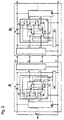
- the device for transmitting data between two electronic devices is further specified in the block diagram in FIG. 3 .
- two devices A, B are interconnected in mirror image by means of their interface lines (U +, U-, D, T).
- Both devices are constructed in the same way; if they differ at all, then only with regard to assemblies not shown in FIG. 3 . To simplify matters, the same components have also been provided with the same reference symbols in both devices.
- the operating voltage source (UB) supplies all components (MP, SP, I) as well as the switching device (S) of the device (A) and also sets the access control line (Z2) to a positive potential, which means that the switching means (S2) of the device ( A) are in the switching state shown in the drawing, in which the signal lines (D, T) of the microprocessor (MP) are connected to the first switching means (S1).
- the operating voltage (UB) also passes through the diode (DI) and the interface (I) of the device (A) and the interface cable (U +, U-) as well as via the interface (I) of the device (B) to the voltage connections of the non-volatile memory (SP) and the switching device (S) of the device (B).
- the switching device of the device (B) is permanently set to the switching state shown in FIG. 3 , in which the signal lines (D, T) of the non-volatile memory (SP) are firmly connected to the interface (I) of the device (B).
- the interface (I) of the device (A) thus has a direct connection to the signal lines of the non-volatile memory (SP) of the device (B) via the interface lines (D, T).
- the microprocessor (MP) of the device (A) now controls, via the access control line (Z1), the first switching means (S1) alternately in a switching state in which the signal lines (D, T) of the microprocessor (MP) with those of the interface (I ) are connected and so the microprocessor (MP) can read data from the interface (I) and then each in a switching state in which the signal lines (D, T) of the microprocessor (MP) with those of the non-volatile memory (SP) of the device (A) are connected, the microprocessor (MP) writing the previously read data into this non-volatile memory (SP).
- SP non-volatile memory
- the complete data record which is contained in the non-volatile memory (SP) of the device (B), is copied in a simple manner into the non-volatile memory (SP) of the device (A). After completing this process, device (A) can be used immediately as a replacement device for a possibly partially defective device (B).
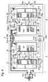
- two devices A, B which are identical with regard to their non-volatile memory organization each have a microprocessor or microcontroller 10 or 20 with ports (inputs and outputs) 10 'or 20' in "Advanced Tristate” or " Power Activated Port Technology ".
- a bidirectional port 10.1 or 21.1 MEM STAT US; MEMSTAT
- a read / write control output 10.2 or 20.2 W RITE / R EAD; W / R
- a bidirectional Data port 10.3 or 20.3 ( DATA ) and a clock output 10.4 or 20.4 ( CL OC K ; CLK) are provided.
- microprocessor or microcontroller 10 or 20 can furthermore have an internal memory area 10.5 or 20.5, which can advantageously comprise a RAM and a ROM for receiving at least one hull part of its boot program.
- an internal memory area 10.5 or 20.5 can advantageously comprise a RAM and a ROM for receiving at least one hull part of its boot program.
- microprocessor can also be replaced by the term “microcontroller”, the latter, as is known, via both analog and digital inputs and / or outputs and can have the required A / D or D / A conversion means.
- the microprocessor or microcontroller 10 or 20 can also cooperate with external RAM and / or ROM modules; For the sake of clarity, those are not shown in the drawing.
- the Corresponding structure of device A or B depends in any case on its application, the scope of programs to be processed and the microprocessor used. If the RAM / ROM of the microprocessor or microcontroller is mentioned below, this can nevertheless be understood as corresponding internal and / or external memory areas within the scope of the invention.
- the device A or B also has a non-volatile memory module 11 or 21, each with an inhibit or disable input 11.1 or 21.1 ( N OT ENA BLE; NENA) in corresponding technology (depending on the logic, this can be the case Input 11.1 or 20.1 is also an enable input ( ENA BLE; ENA), for example in the case of negative logic, which is why this input is designated (N) ENA in the drawing).
- the memory module 11 and 21 has, in addition to the already mentioned input 11.1 or 21.1 or 11.2 or 21.2 an input (WR ITE / R EAD; W / R), a bidirectional data port 11.3 and 21.3 (DATA, DATA) and a clock input 11.4 or 21.4 ( CL OC K ).
- the ports 10 'and 20' of the microprocessor 10 and 20, respectively "Advanced Tristate” or "Power-Activated-Port-Technology” are characterized by the fact that they are also highly resistive in a defined manner when there is no operating voltage U B and are practically negligible as a burden.
- the non-volatile memory module 11 or 21 is designed in such a way that its clock and data inputs and outputs in the inhibit or disable state are high-resistance and also practically negligible as a burden.
- the memory module 11 or 21 is not located directly here, but via a valve 12 or 22 connected upstream in the direction of the supply current flow, on the internal supply voltage rail 18 or 28, which for the sake of simplicity is connected directly to the supply terminal K11 or K21 of device A or B is connected and supported by an energy store 3 or 8 (capacitor) (Normally, of course, there can still be a voltage regulator between the energy store 3 or 8 and the terminals 11 or 21; however, this detail is here
- other components of the device Arang. B are also supplied with operating current from the supply voltage rail 18 or 28 via branching supply lines V10 or V20.
- a resistor or a current source Z10 or Z20 can now be connected to the supply voltage rail 18 or 28, which on the other hand has the above-mentioned point 15 or 25 and in this respect the (N) ENA input 11.1 or 21.1 of the memory module 11 or 21 is connected.
- a (possibly relatively high-resistance) resistor R 11 or R 21 can optionally be connected to ground.
- Exemplary a resistor R 12 or R 22 from the data line 13 or 23 is also connected to ground GND here (also relatively high impedance in practice).
- ports 10.1 and 11.1 or 20.1 and 21.1 can be realized in a leading manner either through a continuous conductor path or via a further valve 16 or 26 which is polarized with respect to its flow direction in such a way that the microprocessor 10 or 20 has the input 11.1 or 21.1 of the relevant memory module 11 or 21 can switch internally in the processor to ground GND.
- device A and B are the supply connection of the memory module 11 and 21, the device ground GND, as well as connections with the data lines 13 and 23 and clock lines 14 and 24 to corresponding contacts KUA or KUB and KGNDA or KGNDB and KDA or KDB and KTA or KTB.
- the respective first-mentioned contacts of device A are connected to the second-mentioned contacts of device B (to be replaced or copied or reproduced) either directly or using a special connecting cable or an adapter C, which one or which here has four paths U +, U- / GND, T and D as an example.
- no electronic interface module is provided here.
- devices A and B can instead be designed in a very targeted manner and in particular with regard to the design of their physical interface and in particular their contacts or their shape in relation to one another and with regard to their accessibility so that two devices A and B are connected Allow said interface also or exclusively - either by means of a very special adapter (for example in the form of an adapter module or copy cable) or only and only directly - to connect or plug together.
- a corresponding adapter therefore preferably does not contain any active semiconductor components, at most in special cases voltage-limiting protective elements of any kind.
- the invention also encompasses that the interface, in addition to mere contacts - for example KUA, KGNDA, KTA, KDA; Possibly also KCA - with these cooperative means, which make an unintentional or unauthorized access to the latter impossible.
- These means can be mechanical and / or integrally connected to the housing of the device.
- an electronic device A has an outer housing which, on the one hand, with respect to its interface, for example contacts KUA, KGNDA, KTA, KDA, possibly also KCA and cooperative means, and vice versa, and on the other hand in relation on a second identical electronic device B and its interface, including contacts KUB, KGNDB, KTB, KDB, possibly also KCB and cooperative means, and vice versa - is designed so that the two interfaces only and only by plugging the two devices together and B, ie at one and the same location, can be connected to one another to form a single, single-body, functional device for data transmission.
- Such training can not only make unintentional damage to the electronics of the device A or B unintentional effects, in particular on the contacts KTA and KTB or KDA and KDB, or at least make it considerably more difficult. It also makes manipulation and abuse very effective.
- Device A or B works as follows - on its own or in conjunction with the other device.
- the resistor or the current source Z10 causes the level "H" at the input 11.1 of the memory module 11, whereby it is initially blocked and at least one of its ports 11.3 (bidirectional data port) and 11.4 (clock input) is switched to high resistance. This takes, for example, the data port 11.3 - possibly supported by the high-resistance resistor R 12 - at the logic level "L".
- the ROM bootstrap of the microprocessor 10 queries the level "H" at its port 10.1 and then or in conjunction with it queries, for example, the aforementioned initial level "L" at its data port 10.3, i.e. the activation of the data line 13. This is done, for example, by the monitored output of a test signal on its data port 10.3.
- the microprocessor interprets a correspondingly positive query as "normal operation".
- the ROM bootstrap is at least the part of the initialization software of the microprocessor in the respective device application that makes the ports, i.e. inputs and outputs of the microprocessor, at least queryable.
- a corresponding query can alternatively or additionally also be carried out at its clock output 10.4, in particular if a bidirectional port of the microprocessor is used for this.
- both devices are connected to one another according to FIG .
- the contacts K20 and K21 of the device B remain disconnected, while the operating voltage U B is applied to the contacts K10 and K11 of the device A. Without operating voltage at the contacts K20 and K21, by blocking the valve 22, the supply rail 28 can be regarded as being connected to ground GND, especially since the memory 23 cannot be recharged or can even have a short circuit, for example, provided that device B is not acts more functional.
- the resistor or the current source Z10 immediately after the supply voltage U B is applied to the terminals K10 and K11 has the level “H” at point 15 and thus at the input 11.1 of the memory module 11, as a result of which the latter is initially blocked and as described its ports 11.3 and 11.4 are switched to high resistance.
- Level (L) is thus at the (N) ENA input 21.1 of the memory module 21, ie the memory module 21 is permanently activated.
- its data line 23 and clock line 24 are electrically connected to the corresponding data line 13 and clock line 14 in device A via a corresponding interface path D or T. Since the microprocessor 20 is not supplied with power, its W / R output 20.2 cannot set the W / R input 21.2 of the memory module 21 to level "H", which in the present case corresponds to actuation of the memory module 21 for reading out.
- the microprocessor 10 first queries the level "H" on its MEMSTAT port 10.1 and then, or in conjunction therewith, checks for the activation of its ports 10.3 and / or 10.4 as a prerequisite for the further normal booting of the application described above Device A.
- the microprocessor 10 interprets this result as an instruction to leave it normal boot routine for the purpose of overwriting current data in the non-volatile memory module 11 with data from the / an external non-volatile memory module 21 (go to clone branching in the bootstrap of the processor).
- the microprocessor 10 does not set its port 10.1 to the "L" level, thereby maintaining the deactivation of the memory module 11, terminates the normal boot process in the state in which readability and readability have been achieved, and at least reads the content of the memory module 21 occupied by data in his RAM.
- the (original) programming of each non-volatile memory chip 11, 21, etc. can be the last bit that can be read out, e.g. provide the level "H” (flag bit). It can thereby be achieved that the data line 23 is at the "H” level at the end of the readout (last bit latch).
- the microprocessor 10 is turned on by its bootstrap and held in a monitoring loop with regard to the level on its data line 13. From this point on, the interface connection can be canceled by C or devices A and B can be electrically separated from one another.
- This separation process is used to trigger the storage of the data read into the RAM of the microprocessor in the non-volatile memory module 11 as follows.
- the microprocessor 10 recognizes this "H-> L" transition (data excess edge) which still occurs after the completion of the reading in on its data line 13 and evaluates it (it) as an instruction "write read data back into the non-volatile memory chip” , consequently sets its MEMSTAT port 10.1 to "L” and its W / R output 10.2 to "H”, thereby activating the memory module 11 for reading in the data previously read into its RAM, and thus indicating this data via line 13 the data port 11.3 of the memory chip 11.3.
- the memory module 11 already has the same data content as the read memory module 21 and the microprocessor sets its W / R output 10.2 back to the "L” level (read).
- the boot program of the microprocessor 10 can be provided in the boot program of the microprocessor 10 that the latter then restart itself.
- the microprocessor 10 boots up the application from the memory 11 as normal after this restart. This is easily possible because, at the time of restart, device B is no longer available and the conditions described under "normal operation" are present.
- the exemplary embodiment described so far also uses synchronous data transmission and manages with only four conductive connections U +, U- / GND, T and D at the interface.
- a modification for asynchronous operation is also possible here, which, however, requires a little more effort.
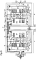
- a simplification is obtained if according to FIG. 5, a fifth connection path CPY (C O PY) provided at the interface, and one is used with pre-integrated A / D converter (microcontroller) as a microprocessor for example.
- the simplification mainly results from the fact that less attention has to be paid when programming the boat rape.
- a voltage divider consisting of two resistors R 14 and R 15 connected in series can be provided lying between the supply rail 18 or 28 and each GND, the central connection of which, on the one hand, to a corresponding A / D input 10.6 or 20.6 of the microcontroller 10 or 20 in question in the device A or B and on the other hand via a path S10 or S20 to a corresponding fifth contact KCA or KCB at the interface.
- the voltage is at said center tap in device A in the absence of device B.
- U R14 1 ⁇ 2U B against ground GND, which falls into a programmed first value window for 1 ⁇ 2U B with, for example, ⁇ 15% tolerance. Presence of the voltage U R14 in this value window is recognized by the microcontroller 10 as a truth condition "B missing" interpreted.
- the microcontroller can therefore only set its MEMSTAT port to the "L" level and thereby activate the memory module 11 when it has found the truth condition in the first voltage window, but this is only possible after the interface path CPY has been opened.
- the monitoring of the data path D after the data have been read into the RAM area of the microcontroller 10 can be omitted here, as can the load bit latch capability of the memory modules 11 and 21 in the activated state after a clock pulse stop.
- Both the second and third exemplary embodiments can be seen in common that the monitoring of a signal level takes the place of a switching device occurs in the target device of the data transfer, this level - at the latest after reading the data from the source memory of device B - can in any case be changed characteristically by the latter in device A regardless of whether device B is defective or not.
- device A If data are to be transferred from device B to device A, in a second step device A is supplied with its normal operating voltage at its normal supply terminals, but not device B. Its supply terminals preferably remain free, but could nevertheless also be short-circuited .
- the non-volatile memory module 11 of the device A is initially inevitably deactivated by energizing it, and the non-volatile memory module 21 of the device B is immediately activated.
- a fourth step the microprocessor of device A recognizes from the immediate activation of a non-volatile memory chip that it is not its own, which is still inactive, and is consequently prompted to read data in the non-volatile memory chip of device B into its RAM area.
- a fifth step the operator waits until the microprocessor of device A has switched to monitoring a signal level after the completion of the read-out process, which signal level (at the latest then) inevitably causes characteristic of the device B in device A to indicate to the microprocessor the presence or absence of device B.
- a sixth step - while maintaining the power supply of device A - the operator disconnects the two devices A and B via their interface.
- this electrical separation is sensed on the basis of the above-mentioned level monitoring and evaluated by the microprocessor of the device A as a truth condition as a truth condition for the now possible writing back of the data previously read into its RAM area in the only non-volatile memory chip still available, namely that of device A.
- the data is written into the aforementioned non-volatile memory chip initiated, carried out and waited by the operator until this registration process is finished.
- a ninth step you can wait until the microprocessor has restarted and / or until the microprocessor has booted up the application of device A as normal and the device has reached normal operational readiness.
- At least part of the bootstrap of the microprocessor can be stored in the non-volatile memory module, with the result that this part is also transferred 1: 1 to the new non-volatile memory module, so that it is never lost and can be used for an automatic correctness check of the data transmission.
- At least one (other) part of the bootstrap can nevertheless be stored in a special ROM area (10.5 or 20.5) of the microprocessor, which can be an integral part of the microprocessor.
- the correctness of the data transmission that has taken place can also be checked in a tenth step in the above-mentioned booting process of the application.
- a new device A takes over the non-volatile data of an old device B, or the latter inevitably "inherits" its data to the new device A.
- a means of transport it is thus ensured, for example, that the new device A is absolutely at the same level as the old device B with regard to stored vehicle parameters and life cycle data. It is thus possible to continue operating seamlessly with the parameters that have accumulated, with the exclusion of any diligence in re-application phases. Replacement logistics are completely eliminated.
- the electronic device according to the invention and the method according to the invention can advantageously also be used to produce devices in any number identically in a simple manner.
Landscapes
- Techniques For Improving Reliability Of Storages (AREA)
- Hardware Redundancy (AREA)
- Communication Control (AREA)
- Power Sources (AREA)
- Arrangements For Transmission Of Measured Signals (AREA)
Applications Claiming Priority (2)
| Application Number | Priority Date | Filing Date | Title |
|---|---|---|---|
| DE19607101A DE19607101A1 (de) | 1996-02-24 | 1996-02-24 | Elektronisches Gerät und Einrichtung zur Datenübertragung zwischen zwei gleichartig aufgebauten elektronischen Geräten |
| DE19607101 | 1996-02-24 |
Publications (3)
| Publication Number | Publication Date |
|---|---|
| EP0791929A2 true EP0791929A2 (fr) | 1997-08-27 |
| EP0791929A3 EP0791929A3 (fr) | 1999-08-18 |
| EP0791929B1 EP0791929B1 (fr) | 2002-11-27 |
Family
ID=7786420
Family Applications (1)
| Application Number | Title | Priority Date | Filing Date |
|---|---|---|---|
| EP96114934A Expired - Lifetime EP0791929B1 (fr) | 1996-02-24 | 1996-09-18 | Dispositif électronique et méthode de sa duplication et système de transfert de données entre deux dispositifs électroniques similaires |
Country Status (4)
| Country | Link |
|---|---|
| US (1) | US5832194A (fr) |
| EP (1) | EP0791929B1 (fr) |
| DE (2) | DE19607101A1 (fr) |
| ES (1) | ES2185731T3 (fr) |
Cited By (1)
| Publication number | Priority date | Publication date | Assignee | Title |
|---|---|---|---|---|
| DE10001260C1 (de) * | 2000-01-14 | 2001-08-30 | Daimler Chrysler Ag | Fahrzeuganordnung mit einem Identitätsspeicher und Herstellugsverfahren hierzu |
Families Citing this family (9)
| Publication number | Priority date | Publication date | Assignee | Title |
|---|---|---|---|---|
| US6058474A (en) * | 1997-01-24 | 2000-05-02 | Texas Instruments Incorporated | Method and apparatus for DMA boot loading a microprocessor without an internal ROM |
| DE19946096A1 (de) * | 1999-09-27 | 2001-04-12 | Mannesmann Vdo Ag | Steuergerät, insbesondere für ein Kraftfahrzeug |
| US6522247B2 (en) * | 2000-05-23 | 2003-02-18 | Kabushiki Kaisha Toshiba | Apparatus monitoring system and apparatus monitoring method |
| US20070058456A1 (en) * | 2005-09-09 | 2007-03-15 | Rico Srowik | Integrated circuit arrangement |
| US8365637B2 (en) * | 2007-10-23 | 2013-02-05 | Caterpillar Inc. | Drop box for powertrain |
| DE102009020731A1 (de) * | 2009-05-11 | 2010-11-25 | Continental Automotive Gmbh | Verfahren und Steuereinheit zum Betreiben eines flüchtigen Speichers, Schaltungsanordnung und Fahrtenschreiber |
| US9383970B2 (en) * | 2009-08-13 | 2016-07-05 | Microsoft Technology Licensing, Llc | Distributed analytics platform |
| JP5418567B2 (ja) * | 2011-10-14 | 2014-02-19 | オンキヨー株式会社 | 受信装置 |
| US11893276B2 (en) * | 2020-05-21 | 2024-02-06 | Micron Technology, Inc. | Apparatuses and methods for data management in a memory device |
Family Cites Families (25)
| Publication number | Priority date | Publication date | Assignee | Title |
|---|---|---|---|---|
| IT1151351B (it) * | 1982-01-19 | 1986-12-17 | Italtel Spa | Disposizione circuitale atta a realizzare lo scambio di dati tra una coppia di elaboratori operanti secondo il principio master-slave |
| JPH0754442B2 (ja) * | 1983-11-24 | 1995-06-07 | 大倉電気株式会社 | プロセス制御システム |
| DE3540599A1 (de) * | 1985-11-15 | 1987-05-21 | Porsche Ag | Diagnosesystem fuer ein kraftfahrzeug |
| JPS63255759A (ja) * | 1987-04-14 | 1988-10-24 | Mitsubishi Electric Corp | 制御システム |
| DE8816458U1 (de) * | 1987-09-02 | 1989-09-14 | Siemens AG, 1000 Berlin und 8000 München | Gerät zur laufenden Überwachung des Betriebes eines Kfz |
| US4937732A (en) * | 1987-10-20 | 1990-06-26 | James Hardie Irrigation, Inc. | Irrigation controller |
| US5083264A (en) * | 1989-04-24 | 1992-01-21 | Xerox Corporation | Process and apparatus for saving and restoring critical files on the disk memory of an electrostatographic reproduction machine |
| DE58908047D1 (de) * | 1989-04-25 | 1994-08-18 | Siemens Ag | Verfahren zur Synchronisation von Datenverarbeitungsanlagen. |
| US5307481A (en) * | 1990-02-28 | 1994-04-26 | Hitachi, Ltd. | Highly reliable online system |
| US5195100A (en) * | 1990-03-02 | 1993-03-16 | Micro Technology, Inc. | Non-volatile memory storage of write operation identifier in data sotrage device |
| US5134619A (en) * | 1990-04-06 | 1992-07-28 | Sf2 Corporation | Failure-tolerant mass storage system |
| US5140592A (en) * | 1990-03-02 | 1992-08-18 | Sf2 Corporation | Disk array system |
| US5210866A (en) * | 1990-09-12 | 1993-05-11 | Storage Technology Corporation | Incremental disk backup system for a dynamically mapped data storage subsystem |
| US5274799A (en) * | 1991-01-04 | 1993-12-28 | Array Technology Corporation | Storage device array architecture with copyback cache |
| US5231872A (en) * | 1991-02-21 | 1993-08-03 | Ttc/Truck Tech Corp. | Tire monitoring apparatus and method |
| CH683652A5 (de) * | 1992-03-10 | 1994-04-15 | Frama Ag | Frankiermaschine. |
| JPH05341918A (ja) * | 1992-05-12 | 1993-12-24 | Internatl Business Mach Corp <Ibm> | 二重化デイスク記憶装置システムを構成するための接続装置 |
| US5412661A (en) * | 1992-10-06 | 1995-05-02 | International Business Machines Corporation | Two-dimensional disk array |
| US5539638A (en) * | 1993-08-05 | 1996-07-23 | Pavilion Technologies, Inc. | Virtual emissions monitor for automobile |
| US5432922A (en) * | 1993-08-23 | 1995-07-11 | International Business Machines Corporation | Digital storage system and method having alternating deferred updating of mirrored storage disks |
| US5600783A (en) * | 1993-11-30 | 1997-02-04 | Hitachi, Ltd. | Disc array system having disc storage devices dispersed on plural boards and accessible at withdrawal of part of the boards |
| US5396620A (en) * | 1993-12-21 | 1995-03-07 | Storage Technology Corporation | Method for writing specific values last into data storage groups containing redundancy |
| US5566316A (en) * | 1994-02-10 | 1996-10-15 | Storage Technology Corporation | Method and apparatus for hierarchical management of data storage elements in an array storage device |
| US5608684A (en) * | 1994-10-13 | 1997-03-04 | Hewlett-Packard Company | System and method for RAM power and data backup utilizing a capacitor and ROM |
| US5680580A (en) * | 1995-02-28 | 1997-10-21 | International Business Machines Corporation | Remote copy system for setting request interconnect bit in each adapter within storage controller and initiating request connect frame in response to the setting bit |
-
1996
- 1996-02-24 DE DE19607101A patent/DE19607101A1/de not_active Ceased
- 1996-09-18 ES ES96114934T patent/ES2185731T3/es not_active Expired - Lifetime
- 1996-09-18 EP EP96114934A patent/EP0791929B1/fr not_active Expired - Lifetime
- 1996-09-18 US US08/710,512 patent/US5832194A/en not_active Expired - Fee Related
- 1996-09-18 DE DE59609919T patent/DE59609919D1/de not_active Expired - Lifetime
Cited By (1)
| Publication number | Priority date | Publication date | Assignee | Title |
|---|---|---|---|---|
| DE10001260C1 (de) * | 2000-01-14 | 2001-08-30 | Daimler Chrysler Ag | Fahrzeuganordnung mit einem Identitätsspeicher und Herstellugsverfahren hierzu |
Also Published As
| Publication number | Publication date |
|---|---|
| DE19607101A1 (de) | 1997-08-28 |
| EP0791929B1 (fr) | 2002-11-27 |
| ES2185731T3 (es) | 2003-05-01 |
| DE59609919D1 (de) | 2003-01-09 |
| EP0791929A3 (fr) | 1999-08-18 |
| US5832194A (en) | 1998-11-03 |
Similar Documents
| Publication | Publication Date | Title |
|---|---|---|
| DE4012109C2 (de) | Vorrichtung zur Funktionsüberwachung eines elektrischen/elektronischen Schaltmittels, seines angeschlossenen Verbrauchers, einer Ansteuerung und seiner Verbindungsleitung | |
| DE10326287B4 (de) | Fahrzeug-Kommunikationssystem, Initialisierungseinheit sowie im Fahrzeug eingebaute Steuereinheit | |
| DE69008283T2 (de) | Gerät zum Nachweis und zur Unterscheidung von funktionellen Fehlern in einer elektrischen Versorgungsschaltung. | |
| DE8817191U1 (de) | Anordnung für definierte Schaltung eines Mikrorechners in Wartebetriebsart | |
| DE10119197A1 (de) | Elektronische Steuereinrichtung für Fahrzeuge | |
| EP1089219A2 (fr) | Méthode de proteger une mémoire de donnée | |
| EP0791929B1 (fr) | Dispositif électronique et méthode de sa duplication et système de transfert de données entre deux dispositifs électroniques similaires | |
| DE102017219390B4 (de) | Elektronische steuereinheit | |
| DE3501194C2 (de) | Verfahren und Vorrichtung zum Datenaustausch zwischen Mikroprozessoren | |
| DE112022006044T5 (de) | Stromversorgungssteuereinrichtung und fehlererkennungsverfahren | |
| DE102007006614A1 (de) | Anwendung einer verteilten Diagnosearchitektur in AUTOSAR | |
| EP0437551B1 (fr) | Procede et dispositif pour l'interrogation de donnees provenant d'appareils de commande | |
| DE69910566T2 (de) | Elektronische integrierte Schaltung mit Trimmmittel und Verfahren dafür | |
| DE69905238T2 (de) | Einrichtung zur vollständigen Diagnose eines Treibers | |
| DE102017219388A1 (de) | Elektronische steuereinheit | |
| DE102018000726B4 (de) | Steuereinheit zur Verwendung in einem Fahrzeug und Verfahren zum Bereitstellen von Notstrom für die Steuereinheit | |
| DE3751374T2 (de) | Verfahren und Mechanismus zum unabhängigen Sicherstellungsmodustransfer für digitale Steuerprozessoren. | |
| DE4429633C2 (de) | Verfahren und Vorrichtung zur Überwachung von Speicherzellen eines Speichers | |
| DE19647131A1 (de) | Vorrichtung und Verfahren zur zeitmultiplexen Übertragung von Informationen | |
| DE19605606B4 (de) | Einrichtung zum Rücksetzen eines Rechenelements | |
| DE102017212918A1 (de) | Verfahren zum Betreiben eines Steuergerätes und Vorrichtung mit zugehörigem Steuergerät | |
| DE102015005971A1 (de) | Elektrisches Steuersystem sowie Verfahren zur Funktionskontrolle des Masseanschlusses einer elektronischen Steuereinheit eines solchen elektrischen Steuersystems | |
| DE10306553B4 (de) | Steuervorrichtung für Kraftfahrzeuge und Verfahren zum Betreiben einer Steuervorrichtung | |
| DE102024210557B3 (de) | Fehlerfallrückschreibung | |
| DE112021005649T5 (de) | Fahrzeugsteuervorrichtung |
Legal Events
| Date | Code | Title | Description |
|---|---|---|---|
| PUAI | Public reference made under article 153(3) epc to a published international application that has entered the european phase |
Free format text: ORIGINAL CODE: 0009012 |
|
| AK | Designated contracting states |
Kind code of ref document: A2 Designated state(s): DE ES FR GB IT NL SE |
|
| RAP1 | Party data changed (applicant data changed or rights of an application transferred) |
Owner name: DAIMLER-BENZ AKTIENGESELLSCHAFT Owner name: HELLA KG HUECK & CO. |
|
| RAP1 | Party data changed (applicant data changed or rights of an application transferred) |
Owner name: DAIMLERCHRYSLER AG Owner name: HELLA KG HUECK & CO. |
|
| PUAL | Search report despatched |
Free format text: ORIGINAL CODE: 0009013 |
|
| AK | Designated contracting states |
Kind code of ref document: A3 Designated state(s): DE ES FR GB IT NL SE |
|
| RIC1 | Information provided on ipc code assigned before grant |
Free format text: 6G 11C 5/00 A, 6G 11C 16/02 B, 6G 06F 11/20 B, 6G 11C 7/00 B |
|
| 17P | Request for examination filed |
Effective date: 19991216 |
|
| 17Q | First examination report despatched |
Effective date: 20010713 |
|
| GRAG | Despatch of communication of intention to grant |
Free format text: ORIGINAL CODE: EPIDOS AGRA |
|
| GRAG | Despatch of communication of intention to grant |
Free format text: ORIGINAL CODE: EPIDOS AGRA |
|
| GRAH | Despatch of communication of intention to grant a patent |
Free format text: ORIGINAL CODE: EPIDOS IGRA |
|
| GRAH | Despatch of communication of intention to grant a patent |
Free format text: ORIGINAL CODE: EPIDOS IGRA |
|
| GRAA | (expected) grant |
Free format text: ORIGINAL CODE: 0009210 |
|
| AK | Designated contracting states |
Kind code of ref document: B1 Designated state(s): DE ES FR GB IT NL SE |
|
| REG | Reference to a national code |
Ref country code: GB Ref legal event code: FG4D Free format text: NOT ENGLISH |
|
| REF | Corresponds to: |
Ref document number: 59609919 Country of ref document: DE Date of ref document: 20030109 |
|
| GBT | Gb: translation of ep patent filed (gb section 77(6)(a)/1977) |
Effective date: 20030315 |
|
| REG | Reference to a national code |
Ref country code: ES Ref legal event code: FG2A Ref document number: 2185731 Country of ref document: ES Kind code of ref document: T3 |
|
| ET | Fr: translation filed | ||
| PGFP | Annual fee paid to national office [announced via postgrant information from national office to epo] |
Ref country code: ES Payment date: 20030910 Year of fee payment: 8 |
|
| PGFP | Annual fee paid to national office [announced via postgrant information from national office to epo] |
Ref country code: NL Payment date: 20030923 Year of fee payment: 8 |
|
| PLBE | No opposition filed within time limit |
Free format text: ORIGINAL CODE: 0009261 |
|
| STAA | Information on the status of an ep patent application or granted ep patent |
Free format text: STATUS: NO OPPOSITION FILED WITHIN TIME LIMIT |
|
| 26N | No opposition filed |
Effective date: 20030828 |
|
| PG25 | Lapsed in a contracting state [announced via postgrant information from national office to epo] |
Ref country code: ES Free format text: LAPSE BECAUSE OF NON-PAYMENT OF DUE FEES Effective date: 20040920 |
|
| PG25 | Lapsed in a contracting state [announced via postgrant information from national office to epo] |
Ref country code: NL Free format text: LAPSE BECAUSE OF NON-PAYMENT OF DUE FEES Effective date: 20050401 |
|
| NLV4 | Nl: lapsed or anulled due to non-payment of the annual fee |
Effective date: 20050401 |
|
| PGFP | Annual fee paid to national office [announced via postgrant information from national office to epo] |
Ref country code: FR Payment date: 20050823 Year of fee payment: 10 |
|
| PGFP | Annual fee paid to national office [announced via postgrant information from national office to epo] |
Ref country code: SE Payment date: 20050906 Year of fee payment: 10 |
|
| PGFP | Annual fee paid to national office [announced via postgrant information from national office to epo] |
Ref country code: GB Payment date: 20050914 Year of fee payment: 10 |
|
| REG | Reference to a national code |
Ref country code: ES Ref legal event code: FD2A Effective date: 20040920 |
|
| PG25 | Lapsed in a contracting state [announced via postgrant information from national office to epo] |
Ref country code: SE Free format text: LAPSE BECAUSE OF NON-PAYMENT OF DUE FEES Effective date: 20060919 |
|
| PGFP | Annual fee paid to national office [announced via postgrant information from national office to epo] |
Ref country code: IT Payment date: 20060930 Year of fee payment: 11 |
|
| EUG | Se: european patent has lapsed | ||
| GBPC | Gb: european patent ceased through non-payment of renewal fee |
Effective date: 20060918 |
|
| REG | Reference to a national code |
Ref country code: FR Ref legal event code: ST Effective date: 20070531 |
|
| PG25 | Lapsed in a contracting state [announced via postgrant information from national office to epo] |
Ref country code: GB Free format text: LAPSE BECAUSE OF NON-PAYMENT OF DUE FEES Effective date: 20060918 |
|
| PG25 | Lapsed in a contracting state [announced via postgrant information from national office to epo] |
Ref country code: FR Free format text: LAPSE BECAUSE OF NON-PAYMENT OF DUE FEES Effective date: 20061002 |
|
| PG25 | Lapsed in a contracting state [announced via postgrant information from national office to epo] |
Ref country code: IT Free format text: LAPSE BECAUSE OF NON-PAYMENT OF DUE FEES Effective date: 20070918 |
|
| PGFP | Annual fee paid to national office [announced via postgrant information from national office to epo] |
Ref country code: DE Payment date: 20150916 Year of fee payment: 20 |
|
| REG | Reference to a national code |
Ref country code: DE Ref legal event code: R071 Ref document number: 59609919 Country of ref document: DE |