EP0792036A1 - Verfahren zur optischen Übertragung von digitalen Daten - Google Patents
Verfahren zur optischen Übertragung von digitalen Daten Download PDFInfo
- Publication number
- EP0792036A1 EP0792036A1 EP97400345A EP97400345A EP0792036A1 EP 0792036 A1 EP0792036 A1 EP 0792036A1 EP 97400345 A EP97400345 A EP 97400345A EP 97400345 A EP97400345 A EP 97400345A EP 0792036 A1 EP0792036 A1 EP 0792036A1
- Authority
- EP
- European Patent Office
- Prior art keywords
- binary value
- phase shift
- phase
- cell containing
- isolated cell
- Prior art date
- Legal status (The legal status is an assumption and is not a legal conclusion. Google has not performed a legal analysis and makes no representation as to the accuracy of the status listed.)
- Granted
Links
- 230000003287 optical effect Effects 0.000 title claims abstract description 31
- 238000000034 method Methods 0.000 title claims abstract description 23
- 230000005540 biological transmission Effects 0.000 title abstract description 16
- 230000010363 phase shift Effects 0.000 claims abstract description 41
- 239000000835 fiber Substances 0.000 abstract description 9
- 239000006185 dispersion Substances 0.000 abstract description 4
- 239000013307 optical fiber Substances 0.000 abstract description 2
- 238000010586 diagram Methods 0.000 description 14
- 230000008033 biological extinction Effects 0.000 description 11
- 230000003111 delayed effect Effects 0.000 description 4
- 230000000750 progressive effect Effects 0.000 description 4
- 230000000630 rising effect Effects 0.000 description 4
- 239000013256 coordination polymer Substances 0.000 description 3
- 238000002347 injection Methods 0.000 description 3
- 239000007924 injection Substances 0.000 description 3
- 238000001228 spectrum Methods 0.000 description 3
- 230000001934 delay Effects 0.000 description 2
- 230000000694 effects Effects 0.000 description 2
- 238000007493 shaping process Methods 0.000 description 2
- 238000004088 simulation Methods 0.000 description 2
- 238000009825 accumulation Methods 0.000 description 1
- 230000015556 catabolic process Effects 0.000 description 1
- 230000000295 complement effect Effects 0.000 description 1
- 230000001186 cumulative effect Effects 0.000 description 1
- 238000006731 degradation reaction Methods 0.000 description 1
- 238000001914 filtration Methods 0.000 description 1
- 238000002955 isolation Methods 0.000 description 1
- 230000003071 parasitic effect Effects 0.000 description 1
- 230000000704 physical effect Effects 0.000 description 1
- 230000010349 pulsation Effects 0.000 description 1
- 230000035945 sensitivity Effects 0.000 description 1
- 230000003595 spectral effect Effects 0.000 description 1
- 230000001360 synchronised effect Effects 0.000 description 1
- 230000001960 triggered effect Effects 0.000 description 1
Images

Classifications
-
- H—ELECTRICITY
- H04—ELECTRIC COMMUNICATION TECHNIQUE
- H04B—TRANSMISSION
- H04B10/00—Transmission systems employing electromagnetic waves other than radio-waves, e.g. infrared, visible or ultraviolet light, or employing corpuscular radiation, e.g. quantum communication
- H04B10/50—Transmitters
- H04B10/516—Details of coding or modulation
- H04B10/5161—Combination of different modulation schemes
-
- H—ELECTRICITY
- H04—ELECTRIC COMMUNICATION TECHNIQUE
- H04B—TRANSMISSION
- H04B10/00—Transmission systems employing electromagnetic waves other than radio-waves, e.g. infrared, visible or ultraviolet light, or employing corpuscular radiation, e.g. quantum communication
- H04B10/25—Arrangements specific to fibre transmission
- H04B10/2507—Arrangements specific to fibre transmission for the reduction or elimination of distortion or dispersion
- H04B10/2513—Arrangements specific to fibre transmission for the reduction or elimination of distortion or dispersion due to chromatic dispersion
- H04B10/25137—Arrangements specific to fibre transmission for the reduction or elimination of distortion or dispersion due to chromatic dispersion using pulse shaping at the transmitter, e.g. pre-chirping or dispersion supported transmission [DST]
-
- H—ELECTRICITY
- H04—ELECTRIC COMMUNICATION TECHNIQUE
- H04B—TRANSMISSION
- H04B10/00—Transmission systems employing electromagnetic waves other than radio-waves, e.g. infrared, visible or ultraviolet light, or employing corpuscular radiation, e.g. quantum communication
- H04B10/50—Transmitters
- H04B10/516—Details of coding or modulation
- H04B10/54—Intensity modulation
- H04B10/541—Digital intensity or amplitude modulation
-
- H—ELECTRICITY
- H04—ELECTRIC COMMUNICATION TECHNIQUE
- H04B—TRANSMISSION
- H04B10/00—Transmission systems employing electromagnetic waves other than radio-waves, e.g. infrared, visible or ultraviolet light, or employing corpuscular radiation, e.g. quantum communication
- H04B10/50—Transmitters
- H04B10/516—Details of coding or modulation
- H04B10/548—Phase or frequency modulation
-
- H—ELECTRICITY
- H04—ELECTRIC COMMUNICATION TECHNIQUE
- H04L—TRANSMISSION OF DIGITAL INFORMATION, e.g. TELEGRAPHIC COMMUNICATION
- H04L27/00—Modulated-carrier systems
- H04L27/32—Carrier systems characterised by combinations of two or more of the types covered by groups H04L27/02, H04L27/10, H04L27/18 or H04L27/26
- H04L27/34—Amplitude- and phase-modulated carrier systems, e.g. quadrature-amplitude modulated carrier systems
- H04L27/36—Modulator circuits; Transmitter circuits
- H04L27/361—Modulation using a single or unspecified number of carriers, e.g. with separate stages of phase and amplitude modulation
Definitions
- the invention relates to the field of digital data transmission by optical means. It relates more particularly to broadband transmission over long distance links using optical fibers.
- Such transmission is effected by means of an optical transmitter connected to an optical receiver via the fiber.
- the transmitter uses an optical carrier wave whose power it modulates according to the information to be transmitted.
- modulation consists in varying the power of the carrier wave between two levels: a low level corresponding to an extinction of the wave and a high level corresponding to the maximum optical power of a laser oscillator.
- the low and high levels represent the binary values "0" and "1" respectively.
- the variations in the level of the wave are triggered at instants imposed by a clock signal which thus defines successive time cells allocated to the data to be transmitted.
- the maximum distance of a transmission is limited by the possibility for the receivers to detect without error these two power levels after propagation of the modulated wave in the optical link.
- the information rate is limited by the chromatic dispersion generated in the fibers.
- This dispersion which results from a dependence of the effective index of the fiber on the wavelength of the transported wave has the consequence that the width of the emitted pulses increases as they propagate along the fiber. .
- duobinary code for optical transmissions was mentioned in the article entitled: "10 Gbit / s unrepeatered three-level optical transmission over 100 km of standard fiber", X.Gu et al, ELECTRONICS LETTERS, December 9, 1993 , Vol. 29, No. 25. According to this article, the three levels 0, +, - correspond respectively to three levels of optical power.
- phase inversion duobinary code is also mentioned in the article "Optical duobinary transmission system with no receiver sensitivity degradation", K. Yonenaga et al, ELECTRONICS LETTERS, February 16, 1995, Vol. 31, No. 4.
- the object of the invention is therefore to propose an optical transmission method exploiting the preceding observations.
- This process can be designated by: "Binary Transmission with Controlled Phase Profile” or by the acronym PSBT (from English: “Phase-Shaped Binary Transmission”).
- the subject of the invention is a method for transmitting binary data contained respectively in the successive time cells, said data being in the form of an optical signal obtained by power modulation of an optical carrier wave, a first and a second. binary value of a data corresponding respectively to a low and high average power inside each cell containing said data, characterized in that a phase shift is applied to said carrier wave inside each cell which contains said first binary value and which precedes or succeeds any block of consecutive cells containing said second binary value or any isolated cell containing said second binary value.
- phase shift takes place in each cell containing a "0" (low level) and close to a block of "1" or an isolated "1".
- the absolute value of the phase shift for an isolated cell is preferably between 90 ° and 180 °.
- the absolute value of the phase shift is preferably between 45 ° and 180 °.
- the phase shifts are carried out instantaneously.
- the phase shift is carried out gradually.
- the method is characterized in that said phase shift not being instantaneous, for each non-isolated cell containing the first binary value and which respectively precedes or succeeds a an isolated cell containing the second binary value or a block of consecutive cells each containing the second binary value, said phase shift corresponds mathematically and / or physically respectively to a negative or positive frequency pulse.
- phase shifts made in successive isolated cells containing the first binary value correspond mathematically alternately to positive and negative frequency pulses of the carrier wave.
- phase shifts are carried out substantially in the middle of the cells.
- the timing diagram a in FIG. 1 represents a succession of binary data to be transmitted.
- This data is for example in the form of electrical pulses E synchronized by a clock signal.
- Each time interval between two successive clock signals is called “time-bit” and defines a time cell C1, C2, Ci delimiting the logic value “0” or “1” depending on whether the level of the signal E is low or high. .
- this binary data is transmitted in the form of an optical signal modulated in power and in phase.
- the timing diagrams b and c respectively represent the variations of the power A 2 and of the phase ⁇ of the optical wave emitted.
- the power A 2 is modulated in response to the signal E so as to present in each cell an average power low S0 or high S1 depending on whether the binary data is worth 0 or 1.
- the power S0 of the low level a a value sufficient to allow interference between neighboring symbols 0 and 1 during the propagation of the modulated wave in the transmission fiber.
- the timing diagram c represents the variations of the phase ⁇ of the transmitted wave with respect to an arbitrary reference.
- a respectively positive or negative phase shift corresponds mathematically to a pulse of frequency respectively positive or negative.
- the offset will be progressive or instantaneous depending on whether the corresponding frequency pulse is finite or infinite.
- phase ⁇ undergoes a variation ⁇ 0 of absolute value PH0 inside each cell containing a 0 isolated and a phase variation ⁇ 1 of absolute value PH1 is imposed inside each cell containing a non-isolated 0 and which precedes or succeeds a cell 1.
- the cumulative phase shift will be limited if the phase shifts ⁇ 0 in the isolated cells 0 are alternately positive and negative.
- phase shifts occur instantaneously.
- This operating mode with a phase shift of approximately 180 °, can be obtained in practice by means of an interferometric assembly of the Mach-Zehnder type for example. Indeed, with such a device, the phase changes occur at times when the supply voltage passes through a determined value which also corresponds to a minimum value of the power of the transmitted wave. It is also possible to carry out progressive phase shifts by using, for example, a phase modulator in accordance with the embodiments which will be described.
- the timing diagrams d and e of FIG. 1 The latter case is illustrated by the timing diagrams d and e of FIG. 1.
- the instantaneous frequency f of the transmitted wave has positive or negative finite impulse variations with respect to the frequency fo of the carrier wave. These frequency variations result in progressive phase shifts ⁇ as shown in the timing diagram e. It can be checked that the variations ⁇ 1 of the phase in the non-isolated cells 0 correspond to positive or negative frequency pulses depending on whether the cell succeeds a falling edge or precedes a rising edge of the amplitude A of the transmitted wave.
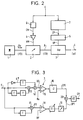
- FIG. 2 is a schematic representation of a first example of implementation of the method according to the invention.
- the optical part essentially consists of a laser oscillator 1 coupled to a power modulator 2 itself coupled to a phase modulator 3.
- the oscillator 1 supplies the power modulator 2 with the carrier wave of amplitude Ap and of frequency fo.
- the power modulator 2 supplies the phase modulator 3 with a wave of variable amplitude A carried by the same frequency fo.
- the phase modulator 3 supplies the transmitted wave S of amplitude A and of phase ⁇ .
- the modulator 2 receives on its electrodes a control voltage VM supplied by an electrical supply circuit 4.
- the phase modulator 3 receives from the electrical circuit 5 a modulation control voltage VP.
- the supply circuits 4 and 5 are variable voltage sources controlled respectively by the control signals CM and CP supplied respectively by the electronic control circuits 6 and 7.
- the circuits 6 and 7 receive the electrical signal E as input having example the form of an NRZ modulation corresponding to the sequence of binary data to be transmitted.
- the circuit 6 can consist of a simple shaping circuit to adapt the levels of the received signal E to the supply circuit 4. It will optionally contain appropriate delay means for synchronizing the commands applied to the modulators 2 and 3.
- circuits 6 and 7 will also include low-pass filtering means making it possible to limit the passband of the modulation.
- the phase control circuit 7 is described in more detail in Figure 3.
- the circuit 7 shown in FIG. 3 comprises a phase control chain CP0 for the isolated "0" (upper part of the diagram) and a phase control chain CP1 for the non-isolated "0" next to a "1" (lower part of the diagram).
- the upper chain comprises a first analog adder 13 receiving the signal E as inputs and the same signal E delayed by two bit-times T.
- a second analog adder 14 receives as input the signal supplied by the adder 13 and the complement E * of the input signal E delayed by a time-bit T.
- the output X0 of the adder 14 is compared with a reference voltage Ru in a differential amplifier 15 operating as a comparator.
- the voltage Ru has a value between three times and twice the high level of the signal E.
- the output of the amplifier 15 is applied to the input of a frequency divider by two 16 whose output is connected to one of the inputs of an analog output adder 20.
- the non-isolated "0" control chain comprises an analog adder 17 receiving the input signal E and the input signal E delayed by a bit time T.
- the signal X1 supplied by the adder 17 is compared to a second reference voltage Rf in a second differential amplifier 18 operating as a comparator.
- the voltage Rf is between the low and high levels of the signal E.
- the output of the amplifier 18 is connected via a variable delay device T1 to a variable attenuator 19 whose output signal CP1 is applied to the second input of the adder 20.
- the output of the adder is connected to another variable delay device ⁇ T which supplies the phase control signal CP as an output.
- the comparator 15 supplies a pulse of a time-bit T in the presence of an isolated "0".
- the signal CP0 at the output of the divider 16 changes status whenever an isolated "0" is detected.
- the output of comparator 18 changes state each time a non-isolated "0" precedes or succeeds a "1".
- the variable delays T1 and ⁇ T are used to reset the signals CP1 and CP0 with respect to the amplitude control signal CM.
- the attenuator 19 is provided for adjusting the respective amplitudes PH0 and PH1 of the phase shifts A ⁇ 0 and A ⁇ 1.
- the phase control signal CP has variations as a function of time similar to those of phase ⁇ , as represented by the timing diagram e in FIG. 1.
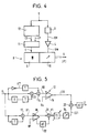
- the optical part 8 only comprises a laser oscillator 9 optically coupled to a power modulator 10.
- the assembly can simply consist of a laser with integrated modulator of a known type .
- the laser part 9 receives an injection current I supplied by a supply circuit 11.
- the modulator 10 receives the voltage VM from the supply circuit 4.
- the circuits 11 and 4 are controlled respectively by the signals CI and CM supplied respectively by a frequency pulse control circuit 12 and the power modulation control circuit 6.
- the control circuits 12 and 6 receive the electrical signal E.
- the phase modulation is carried out here by acting on the injection current I of the laser 9.
- This embodiment uses the property of the lasers to oscillate at a variable frequency as a function of the injection current.
- the laser will be designed so that a small current variation results in a sufficient frequency variation without the power of the transmitted wave undergoing appreciable fluctuations.
- a modulator designed to introduce a minimum chirp will advantageously be chosen.
- the supply circuit 11 essentially consists of a modular current source around a bias current Ip.
- the supply circuit 4 is a variable voltage source as a function of the signal CM supplied by the control circuit 6.
- the circuit 6 is a shaping circuit that can integrate the variable delay function and low pass filter.
- the frequency pulse control circuit 12 is shown in more detail in FIG. 5. It comprises a frequency pulse control chain for the isolated “0" (upper part) and a pulse control chain frequency for non-isolated "0" neighbors of a "1" (lower part).
- the upper part is identical to that of the previous embodiment with the difference that the frequency divider 16 is absent.
- the analog adder 17 receiving the input signal E and the signal E delayed by a time-bit T, as well as the comparator 18 receiving the output signal X1 from the adder 17 and the reference Rf.
- the direct output of comparator 18 is connected to a first input of a fourth analog adder 21.
- the inverting output of comparator 18 is connected to the second input of adder 21 via a delay device 22.
- the signal Y1 supplied by the adder 21 is connected to the attenuator 19 via the variable delay device T1.
- the attenuator 19 supplies the signal CI1 which is received by one of the inputs of the output adder 20, the second input of which receives the signal CI0 supplied by the comparator 15.
- the output signal of the adder 20 is applied to a device with variable delay ⁇ T whose output provides the frequency pulse control signal CI.
- the signal CI0 supplied by the comparator 15 has the form of a pulse of duration equal to the time-bit T each time that an isolated 0 is detected.
- the direct output of comparator 18 changes state each time a non-isolated 0 precedes or follows a falling or rising edge of signal E.
- the delay dT imposed by the device 22 being less than a time-bit T
- the signal Y1 supplied by the adder 21 is formed of alternately positive and negative pulses each time a non-isolated "0" follows or precedes a falling or rising edge respectively of signal E.
- the delays T1 and ⁇ T make it possible to calibrate the signals CI0 and CI1 with respect to the signal CM.
- the attenuator 19 is used to calibrate the pulses of the signal CI1 with respect to those of the signal CI0.
- the signal CI supplied by the circuit 12 has the form of positive and negative pulses analogous to the pulses of frequency f represented on the timing diagram d of FIG. 1, with the difference that the frequency pulses in the isolated "0" are always of the same sign. Indeed, with this embodiment, it is useless to provide alternating signs.
- the conventional NRZ modulation method limits the transmission distance to less than 150 km, while the method of the invention makes it possible to reach 300 km. .
- PH0 is preferably greater than PH1, the ranges of effective values for PH0 and PH1 being respectively 90 ° to 180 ° and 45 ° to 180 °.
Landscapes
- Engineering & Computer Science (AREA)
- Computer Networks & Wireless Communication (AREA)
- Signal Processing (AREA)
- Physics & Mathematics (AREA)
- Electromagnetism (AREA)
- Optical Communication System (AREA)
- Optical Fibers, Optical Fiber Cores, And Optical Fiber Bundles (AREA)
Applications Claiming Priority (2)
| Application Number | Priority Date | Filing Date | Title |
|---|---|---|---|
| FR9602275A FR2745451B1 (fr) | 1996-02-23 | 1996-02-23 | Procede de transmission optique de donnees numeriques |
| FR9602275 | 1996-02-23 |
Publications (2)
| Publication Number | Publication Date |
|---|---|
| EP0792036A1 true EP0792036A1 (de) | 1997-08-27 |
| EP0792036B1 EP0792036B1 (de) | 2003-10-08 |
Family
ID=9489521
Family Applications (1)
| Application Number | Title | Priority Date | Filing Date |
|---|---|---|---|
| EP97400345A Expired - Lifetime EP0792036B1 (de) | 1996-02-23 | 1997-02-17 | Verfahren zur optischen Übertragung von digitalen Daten |
Country Status (7)
| Country | Link |
|---|---|
| US (1) | US5920416A (de) |
| EP (1) | EP0792036B1 (de) |
| JP (1) | JP3268994B2 (de) |
| CA (1) | CA2198270C (de) |
| DE (1) | DE69725360T2 (de) |
| ES (1) | ES2205140T3 (de) |
| FR (1) | FR2745451B1 (de) |
Cited By (1)
| Publication number | Priority date | Publication date | Assignee | Title |
|---|---|---|---|---|
| FR2781322A1 (fr) * | 1998-07-20 | 2000-01-21 | Alsthom Cge Alcatel | Dispositif d'emission de donnees optiques |
Families Citing this family (79)
| Publication number | Priority date | Publication date | Assignee | Title |
|---|---|---|---|---|
| SE515536C2 (sv) * | 1995-08-16 | 2001-08-27 | Ericsson Telefon Ab L M | Kompensation av dispersion |
| JP3027944B2 (ja) * | 1996-08-16 | 2000-04-04 | 日本電気株式会社 | 光デュオバイナリ信号光の生成方法および光送信装置 |
| JP3094950B2 (ja) * | 1997-05-28 | 2000-10-03 | 日本電気株式会社 | 光送信装置及び光送信方法 |
| US6388786B1 (en) | 1997-08-15 | 2002-05-14 | Nec Corporation | Method for generating duobinary signal and optical transmitter using the same method |
| EP1202476B1 (de) * | 2000-10-27 | 2006-08-30 | Alcatel | System und Vorrichtung zum Senden von optischen Daten |
| IT1319558B1 (it) * | 2000-12-15 | 2003-10-20 | Marconi Comm Spa | Schema di codifica di linea per comunicazioni digitali, metodo ditrasmissione e apparato. |
| US6469816B1 (en) | 2001-05-24 | 2002-10-22 | Oyster Optics, Inc. | Phase-modulated fiber optic telecommunications system |
| US6476952B1 (en) | 2001-01-17 | 2002-11-05 | Oyster Optics, Inc. | Phase-modulated fiber optic telecommunications system |
| US6490069B1 (en) | 2001-01-29 | 2002-12-03 | Stratalight Communications, Inc. | Transmission and reception of duobinary multilevel pulse-amplitude-modulated optical signals using subtraction-based encoder |
| US6424444B1 (en) | 2001-01-29 | 2002-07-23 | Stratalight Communications, Inc. | Transmission and reception of duobinary multilevel pulse-amplitude-modulated optical signals using finite-state machine-based encoder |
| US6445476B1 (en) | 2001-01-29 | 2002-09-03 | Stratalight Communications, Inc. | Transmission and reception of duobinary multilevel pulse-amplitude-modulated optical signals using subsequence-based encoder |
| US6665500B2 (en) | 2001-01-29 | 2003-12-16 | Oyster Optics, Inc. | Dual-mode fiber optic telecommunications system and method |
| US7099592B2 (en) | 2001-02-02 | 2006-08-29 | Oyster Optics, Inc. | Telecommunications card for secure optical data transmission and installation method |
| US20020131106A1 (en) * | 2001-03-16 | 2002-09-19 | Peter Snawerdt | Secure wave-division multiplexing telecommunications system and method |
| US6643471B2 (en) | 2001-04-02 | 2003-11-04 | Adc Telecommunications, Inc. | Increased transmission capacity for a fiber-optic link |
| US7085500B2 (en) * | 2001-04-30 | 2006-08-01 | Lockheed Martin Corp. | Programmable optical vector modulator and method for use in coherent optical communications |
| EP1405444B1 (de) * | 2001-07-09 | 2013-01-23 | TQ Gamma, LLC | Faseroptische telekommunikationskarte mit sicherheitserkennung |
| FR2832228B1 (fr) * | 2001-11-12 | 2004-11-19 | Cit Alcatel | Systeme de transmission optique |
| US6623188B1 (en) | 2002-02-08 | 2003-09-23 | Optiuh Corporation | Dispersion tolerant optical data transmitter |
| US6963685B2 (en) * | 2002-07-09 | 2005-11-08 | Daniel Mahgerefteh | Power source for a dispersion compensation fiber optic system |
| US7663762B2 (en) * | 2002-07-09 | 2010-02-16 | Finisar Corporation | High-speed transmission system comprising a coupled multi-cavity optical discriminator |
| US7263291B2 (en) * | 2002-07-09 | 2007-08-28 | Azna Llc | Wavelength division multiplexing source using multifunctional filters |
| US7054538B2 (en) * | 2002-10-04 | 2006-05-30 | Azna Llc | Flat dispersion frequency discriminator (FDFD) |
| US7505694B2 (en) * | 2002-11-06 | 2009-03-17 | Finisar Corporation | Thermal chirp compensation systems for a chirp managed directly modulated laser (CML™) data link |
| US7433605B2 (en) * | 2002-11-06 | 2008-10-07 | Finisar Corporation | Adiabatic frequency modulated transmitter with negative chirp |
| US7564889B2 (en) * | 2002-11-06 | 2009-07-21 | Finisar Corporation | Adiabatically frequency modulated source |
| US7406267B2 (en) * | 2002-11-06 | 2008-07-29 | Finisar Corporation | Method and apparatus for transmitting a signal using thermal chirp management of a directly modulated transmitter |
| US7742542B2 (en) * | 2002-11-06 | 2010-06-22 | Finisar Corporation | Phase correlated quadrature amplitude modulation |
| US7280721B2 (en) * | 2002-11-06 | 2007-10-09 | Azna Llc | Multi-ring resonator implementation of optical spectrum reshaper for chirp managed laser technology |
| US7406266B2 (en) * | 2002-11-06 | 2008-07-29 | Finisar Corporation | Flat-topped chirp induced by optical filter edge |
| US7376352B2 (en) * | 2002-11-06 | 2008-05-20 | Finisar Corporation | Chirp managed laser fiber optic system including an adaptive receiver |
| US7187821B2 (en) | 2002-11-06 | 2007-03-06 | Yasuhiro Matsui | Carrier suppression using adiabatic frequency modulation (AFM) |
| US7536113B2 (en) * | 2002-11-06 | 2009-05-19 | Finisar Corporation | Chirp managed directly modulated laser with bandwidth limiting optical spectrum reshaper |
| US7356264B2 (en) * | 2002-11-06 | 2008-04-08 | Azna Llc | Chirp managed laser with electronic pre-distortion |
| US7352968B2 (en) * | 2002-11-06 | 2008-04-01 | Finisar Corporation | Chirped managed, wavelength multiplexed, directly modulated sources using an arrayed waveguide grating (AWG) as multi-wavelength discriminator |
| US7555225B2 (en) * | 2002-11-06 | 2009-06-30 | Finisar Corporation | Optical system comprising an FM source and a spectral reshaping element |
| US7558488B2 (en) * | 2002-11-06 | 2009-07-07 | Finisar Corporation | Reach extension by using external Bragg grating for spectral filtering |
| US6804472B1 (en) | 2002-11-18 | 2004-10-12 | Stratalight Communications, Inc. | Transmitter and method using half rate data streams for generating full rate modulation on an optical signal |
| US7907648B2 (en) * | 2002-12-03 | 2011-03-15 | Finisar Corporation | Optical FM source based on intra-cavity phase and amplitude modulation in lasers |
| US7480464B2 (en) * | 2002-12-03 | 2009-01-20 | Finisar Corporation | Widely tunable, dispersion tolerant transmitter |
| US7925172B2 (en) * | 2002-12-03 | 2011-04-12 | Finisar Corporation | High power, low distortion directly modulated laser transmitter |
| US7809280B2 (en) * | 2002-12-03 | 2010-10-05 | Finisar Corporation | Chirp-managed, electroabsorption-modulated laser |
| US7474859B2 (en) * | 2002-12-03 | 2009-01-06 | Finisar Corporation | Versatile compact transmitter for generation of advanced modulation formats |
| US7613401B2 (en) * | 2002-12-03 | 2009-11-03 | Finisar Corporation | Optical FM source based on intra-cavity phase and amplitude modulation in lasers |
| US7813648B2 (en) * | 2002-12-03 | 2010-10-12 | Finisar Corporation | Method and apparatus for compensating for fiber nonlinearity in a transmission system |
| US7542683B2 (en) | 2002-12-03 | 2009-06-02 | Finisar Corporation | Chirp Managed Laser (CML) transmitter |
| US7609977B2 (en) * | 2002-12-03 | 2009-10-27 | Finisar Corporation | Optical transmission using semiconductor optical amplifier (SOA) |
| US7860404B2 (en) * | 2002-12-03 | 2010-12-28 | Finisar Corporation | Optical FM source based on intra-cavity phase and amplitude modulation in lasers |
| US8792531B2 (en) | 2003-02-25 | 2014-07-29 | Finisar Corporation | Optical beam steering for tunable laser applications |
| US7630425B2 (en) * | 2003-02-25 | 2009-12-08 | Finisar Corporation | Optical beam steering for tunable laser applications |
| FR2859056B1 (fr) * | 2003-08-19 | 2005-09-30 | Cit Alcatel | Methode de formation d'un signal optique code suivant un format retour a zero ou non retour a zero |
| EP1585235A1 (de) * | 2004-04-08 | 2005-10-12 | Alcatel | Verfahren zur Übertragung von digitalen Signalen über ein optisches Übertragungssystem |
| DE602004003468T2 (de) * | 2004-04-08 | 2007-03-29 | Alcatel | Verfahren zur Übertragung von digitalen Signalen über ein optisches Übertragungssystem |
| KR100606030B1 (ko) * | 2004-07-20 | 2006-07-28 | 삼성전자주식회사 | 듀오바이너리 광 전송장치 및 전송방법 |
| US7639955B2 (en) * | 2004-09-02 | 2009-12-29 | Finisar Corporation | Method and apparatus for transmitting a signal using a chirp managed laser (CML) and an optical spectrum reshaper (OSR) before an optical receiver |
| EP1686706B1 (de) * | 2005-02-01 | 2007-05-30 | Alcatel Lucent | Optischer Sender und Verfahren zur Modulation eines optischen Signals |
| EP1710936B1 (de) * | 2005-04-04 | 2008-09-03 | Alcatel Lucent | Betriebsverfahren für ein passives optisches Netzwerk |
| US20070012860A1 (en) * | 2005-05-05 | 2007-01-18 | Daniel Mahgerefteh | Optical source with ultra-low relative intensity noise (RIN) |
| US20070116476A1 (en) * | 2005-11-18 | 2007-05-24 | Futurewei Technologies, Inc. | Method and apparatus for generating optical duo binary signals with frequency chirp |
| KR100713417B1 (ko) * | 2005-12-02 | 2007-05-04 | 삼성전자주식회사 | 광 송신 모듈 |
| US7697186B2 (en) * | 2006-10-24 | 2010-04-13 | Finisar Corporation | Spectral response modification via spatial filtering with optical fiber |
| WO2008080171A1 (en) | 2006-12-22 | 2008-07-03 | Finisar Corporation | Optical transmitter having a widely tunable directly modulated laser and periodic optical spectrum reshaping element |
| US7941057B2 (en) * | 2006-12-28 | 2011-05-10 | Finisar Corporation | Integral phase rule for reducing dispersion errors in an adiabatically chirped amplitude modulated signal |
| US8131157B2 (en) * | 2007-01-22 | 2012-03-06 | Finisar Corporation | Method and apparatus for generating signals with increased dispersion tolerance using a directly modulated laser transmitter |
| WO2008097928A1 (en) | 2007-02-02 | 2008-08-14 | Finisar Corporation | Temperature stabilizing packaging for optoelectronic components in a transmitter module |
| US8027593B2 (en) | 2007-02-08 | 2011-09-27 | Finisar Corporation | Slow chirp compensation for enhanced signal bandwidth and transmission performances in directly modulated lasers |
| US7991291B2 (en) | 2007-02-08 | 2011-08-02 | Finisar Corporation | WDM PON based on DML |
| US7697847B2 (en) * | 2007-04-02 | 2010-04-13 | Finisar Corporation | Dispersion compensator for frequency reshaped optical signals |
| US7991297B2 (en) * | 2007-04-06 | 2011-08-02 | Finisar Corporation | Chirped laser with passive filter element for differential phase shift keying generation |
| US8204386B2 (en) * | 2007-04-06 | 2012-06-19 | Finisar Corporation | Chirped laser with passive filter element for differential phase shift keying generation |
| US7760777B2 (en) * | 2007-04-13 | 2010-07-20 | Finisar Corporation | DBR laser with improved thermal tuning efficiency |
| US7778295B2 (en) * | 2007-05-14 | 2010-08-17 | Finisar Corporation | DBR laser with improved thermal tuning efficiency |
| US8160455B2 (en) * | 2008-01-22 | 2012-04-17 | Finisar Corporation | Method and apparatus for generating signals with increased dispersion tolerance using a directly modulated laser transmitter |
| US8260145B2 (en) | 2008-03-12 | 2012-09-04 | Deepnarayan Gupta | Digital radio frequency tranceiver system and method |
| US7869473B2 (en) * | 2008-03-21 | 2011-01-11 | Finisar Corporation | Directly modulated laser with isolated modulated gain electrode for improved frequency modulation |
| US8260150B2 (en) * | 2008-04-25 | 2012-09-04 | Finisar Corporation | Passive wave division multiplexed transmitter having a directly modulated laser array |
| US8508864B2 (en) * | 2008-08-25 | 2013-08-13 | Acm Projektentwicklung Gmbh | Objective lens system |
| US7880978B2 (en) * | 2008-08-25 | 2011-02-01 | Acm Projektentwicklung Gmbh | Objective lens system |
| US8199785B2 (en) | 2009-06-30 | 2012-06-12 | Finisar Corporation | Thermal chirp compensation in a chirp managed laser |
Citations (1)
| Publication number | Priority date | Publication date | Assignee | Title |
|---|---|---|---|---|
| FR2719175A1 (fr) | 1994-04-20 | 1995-10-27 | Cit Alcatel | Procédé de transmission optique présentant une sensibilité réduite à la dispersion, et système de transmission pour la mise en Óoeuvre de ce procédé. |
Family Cites Families (1)
| Publication number | Priority date | Publication date | Assignee | Title |
|---|---|---|---|---|
| FR2685834B1 (fr) * | 1991-12-31 | 1995-03-31 | France Telecom | Systeme de transmission numerique longue distance sur fibre optique a compensation a l'emission des distorsions. |
-
1996
- 1996-02-23 FR FR9602275A patent/FR2745451B1/fr not_active Expired - Lifetime
-
1997
- 1997-02-17 EP EP97400345A patent/EP0792036B1/de not_active Expired - Lifetime
- 1997-02-17 ES ES97400345T patent/ES2205140T3/es not_active Expired - Lifetime
- 1997-02-17 DE DE69725360T patent/DE69725360T2/de not_active Expired - Lifetime
- 1997-02-21 CA CA002198270A patent/CA2198270C/fr not_active Expired - Fee Related
- 1997-02-21 JP JP03801697A patent/JP3268994B2/ja not_active Expired - Fee Related
- 1997-02-21 US US08/803,129 patent/US5920416A/en not_active Expired - Lifetime
Patent Citations (2)
| Publication number | Priority date | Publication date | Assignee | Title |
|---|---|---|---|---|
| FR2719175A1 (fr) | 1994-04-20 | 1995-10-27 | Cit Alcatel | Procédé de transmission optique présentant une sensibilité réduite à la dispersion, et système de transmission pour la mise en Óoeuvre de ce procédé. |
| WO1995029539A1 (fr) * | 1994-04-20 | 1995-11-02 | Alcatel Cit | Procede de transmission optique presentant une sensibilite reduite a la dispersion; dispositif et systeme de transmission pour la mise en ×uvre de ce procede |
Non-Patent Citations (1)
| Title |
|---|
| YONENAGA K ET AL: "OPTICAL DUOBINARY TRANSMISSION SYSTEM WITH NO RECEIVER SENSITIVITY DEGRADATION", ELECTRONICS LETTERS, vol. 31, no. 4, 16 February 1995 (1995-02-16), pages 302 - 304, XP000513693 * |
Cited By (3)
| Publication number | Priority date | Publication date | Assignee | Title |
|---|---|---|---|---|
| FR2781322A1 (fr) * | 1998-07-20 | 2000-01-21 | Alsthom Cge Alcatel | Dispositif d'emission de donnees optiques |
| EP0975107A1 (de) * | 1998-07-20 | 2000-01-26 | Alcatel | Sendevorrichtung für optische Daten |
| US6563623B1 (en) | 1998-07-20 | 2003-05-13 | Alcatel | System for transmitting optical data |
Also Published As
| Publication number | Publication date |
|---|---|
| FR2745451B1 (fr) | 1998-04-17 |
| FR2745451A1 (fr) | 1997-08-29 |
| JP3268994B2 (ja) | 2002-03-25 |
| CA2198270C (fr) | 2002-07-23 |
| DE69725360T2 (de) | 2004-08-19 |
| CA2198270A1 (fr) | 1997-08-24 |
| JPH09247087A (ja) | 1997-09-19 |
| EP0792036B1 (de) | 2003-10-08 |
| ES2205140T3 (es) | 2004-05-01 |
| US5920416A (en) | 1999-07-06 |
| DE69725360D1 (de) | 2003-11-13 |
Similar Documents
| Publication | Publication Date | Title |
|---|---|---|
| EP0792036B1 (de) | Verfahren zur optischen Übertragung von digitalen Daten | |
| EP0975107B1 (de) | Sendevorrichtung für optische Daten | |
| CA2220603C (fr) | Dispositif d'emission de donnees optiques | |
| EP0783215B1 (de) | Optisches Übertragungssystem mit Verschlüsselung auf Basis von deterministischem Chaos | |
| EP1111820A1 (de) | Einrichtung zum Anbringen von einer Verzögerung | |
| FR2724510A1 (fr) | Systeme de transmission optique | |
| FR2732123A1 (fr) | Procede de modulation d'impulsions optiques avec compression et systeme de modulation pour la mise en oeuvre de ce procede | |
| EP0576358B1 (de) | Verfahren und Vorrichtung zur optischen Übertragung von Solitonen über lange Abstände | |
| CA2093991C (fr) | Source d'impulsion optique et systeme de transmission optique a solitons comportant cette source | |
| FR2719957A1 (fr) | Procédé pour la transmission d'informations codées sous forme binaire par un train de solitons. | |
| EP0618698A1 (de) | Optische Vorrichtung zur Taktrückgewinnung eines kodierten Signales | |
| EP0630123B1 (de) | Einrichtung zur Regenerierung eines Impulszuges und Einrichtung zur Rückgewinnung eines zu einem modulierten Impulszug synchronisierten periodischen Signals | |
| EP0744844B1 (de) | Binärdateneinschreibungsverfahren, insbesondere optisches, und Vorrichtung zur Durchführung dieses Verfahrens | |
| FR2774762A1 (fr) | Procede et dispositif pour mesurer le spectre complexe (amplitude et phase) d'impulsions optiques | |
| EP0716486A1 (de) | Wellenlängenkonvertor | |
| EP3987692B1 (de) | Kohärente detektion mit optimiertem lokalen oszillator | |
| EP1497939A1 (de) | Optische vorrichtung und verfahren zur umwandlung eines wdm-signals in ein otdm-signal und umgekehrt | |
| EP1508984B1 (de) | Verfahren zur Bildung von einem kodierten RZ oder NRZ Signal | |
| EP1324056B1 (de) | Optischer Impulsgeber mit hoher Extinktionsrate und Abtastsystem insbesondere für Mikrowellensignale | |
| FR3103983A1 (fr) | Détection cohérente avec oscillateur local optimisé | |
| FR3061783A1 (fr) | Modulateur optique dote de diodes mach-zender de longueur reduite | |
| Alic | Information processing for improved performance of optical networks | |
| EP1021004A1 (de) | Verfahren und Vorrichtung zur Stabilisierung von optischen Solitonen | |
| EP0544564A1 (de) | Breitbandige optische Übertragungseinrichtung für mehrere transiente analoge Signale | |
| FR2850222A1 (fr) | Systeme de transmission optique, notamment pour le deport par fibres optiques de signaux x-dsl |
Legal Events
| Date | Code | Title | Description |
|---|---|---|---|
| PUAI | Public reference made under article 153(3) epc to a published international application that has entered the european phase |
Free format text: ORIGINAL CODE: 0009012 |
|
| AK | Designated contracting states |
Kind code of ref document: A1 Designated state(s): DE ES FI GB IT NL SE |
|
| 17P | Request for examination filed |
Effective date: 19980227 |
|
| GRAH | Despatch of communication of intention to grant a patent |
Free format text: ORIGINAL CODE: EPIDOS IGRA |
|
| GRAS | Grant fee paid |
Free format text: ORIGINAL CODE: EPIDOSNIGR3 |
|
| GRAA | (expected) grant |
Free format text: ORIGINAL CODE: 0009210 |
|
| RAP1 | Party data changed (applicant data changed or rights of an application transferred) |
Owner name: ALCATEL |
|
| AK | Designated contracting states |
Kind code of ref document: B1 Designated state(s): DE ES FI GB IT NL SE |
|
| PG25 | Lapsed in a contracting state [announced via postgrant information from national office to epo] |
Ref country code: NL Free format text: LAPSE BECAUSE OF FAILURE TO SUBMIT A TRANSLATION OF THE DESCRIPTION OR TO PAY THE FEE WITHIN THE PRESCRIBED TIME-LIMIT Effective date: 20031008 Ref country code: FI Free format text: LAPSE BECAUSE OF FAILURE TO SUBMIT A TRANSLATION OF THE DESCRIPTION OR TO PAY THE FEE WITHIN THE PRESCRIBED TIME-LIMIT Effective date: 20031008 |
|
| REG | Reference to a national code |
Ref country code: GB Ref legal event code: FG4D Free format text: NOT ENGLISH |
|
| GBT | Gb: translation of ep patent filed (gb section 77(6)(a)/1977) |
Effective date: 20031008 |
|
| REF | Corresponds to: |
Ref document number: 69725360 Country of ref document: DE Date of ref document: 20031113 Kind code of ref document: P |
|
| PG25 | Lapsed in a contracting state [announced via postgrant information from national office to epo] |
Ref country code: SE Free format text: LAPSE BECAUSE OF FAILURE TO SUBMIT A TRANSLATION OF THE DESCRIPTION OR TO PAY THE FEE WITHIN THE PRESCRIBED TIME-LIMIT Effective date: 20040108 |
|
| NLV1 | Nl: lapsed or annulled due to failure to fulfill the requirements of art. 29p and 29m of the patents act | ||
| REG | Reference to a national code |
Ref country code: ES Ref legal event code: FG2A Ref document number: 2205140 Country of ref document: ES Kind code of ref document: T3 |
|
| PLBE | No opposition filed within time limit |
Free format text: ORIGINAL CODE: 0009261 |
|
| STAA | Information on the status of an ep patent application or granted ep patent |
Free format text: STATUS: NO OPPOSITION FILED WITHIN TIME LIMIT |
|
| 26N | No opposition filed |
Effective date: 20040709 |
|
| REG | Reference to a national code |
Ref country code: GB Ref legal event code: 732E Free format text: REGISTERED BETWEEN 20131114 AND 20131120 |
|
| PGFP | Annual fee paid to national office [announced via postgrant information from national office to epo] |
Ref country code: ES Payment date: 20150225 Year of fee payment: 19 Ref country code: IT Payment date: 20150226 Year of fee payment: 19 Ref country code: DE Payment date: 20150219 Year of fee payment: 19 |
|
| PGFP | Annual fee paid to national office [announced via postgrant information from national office to epo] |
Ref country code: GB Payment date: 20150218 Year of fee payment: 19 |
|
| REG | Reference to a national code |
Ref country code: DE Ref legal event code: R119 Ref document number: 69725360 Country of ref document: DE |
|
| GBPC | Gb: european patent ceased through non-payment of renewal fee |
Effective date: 20160217 |
|
| PG25 | Lapsed in a contracting state [announced via postgrant information from national office to epo] |
Ref country code: IT Free format text: LAPSE BECAUSE OF NON-PAYMENT OF DUE FEES Effective date: 20160217 |
|
| PG25 | Lapsed in a contracting state [announced via postgrant information from national office to epo] |
Ref country code: GB Free format text: LAPSE BECAUSE OF NON-PAYMENT OF DUE FEES Effective date: 20160217 Ref country code: DE Free format text: LAPSE BECAUSE OF NON-PAYMENT OF DUE FEES Effective date: 20160901 |
|
| REG | Reference to a national code |
Ref country code: ES Ref legal event code: FD2A Effective date: 20180507 |
|
| PG25 | Lapsed in a contracting state [announced via postgrant information from national office to epo] |
Ref country code: ES Free format text: LAPSE BECAUSE OF NON-PAYMENT OF DUE FEES Effective date: 20160218 |