EP0792079A1 - Architecture d'interface V5 - Google Patents
Architecture d'interface V5 Download PDFInfo
- Publication number
- EP0792079A1 EP0792079A1 EP96113533A EP96113533A EP0792079A1 EP 0792079 A1 EP0792079 A1 EP 0792079A1 EP 96113533 A EP96113533 A EP 96113533A EP 96113533 A EP96113533 A EP 96113533A EP 0792079 A1 EP0792079 A1 EP 0792079A1
- Authority
- EP
- European Patent Office
- Prior art keywords
- lap
- protocol
- protocol manager
- frame
- manager means
- Prior art date
- Legal status (The legal status is an assumption and is not a legal conclusion. Google has not performed a legal analysis and makes no representation as to the accuracy of the status listed.)
- Withdrawn
Links
Images


Classifications
-
- H—ELECTRICITY
- H04—ELECTRIC COMMUNICATION TECHNIQUE
- H04Q—SELECTING
- H04Q11/00—Selecting arrangements for multiplex systems
- H04Q11/04—Selecting arrangements for multiplex systems for time-division multiplexing
- H04Q11/0428—Integrated services digital network, i.e. systems for transmission of different types of digitised signals, e.g. speech, data, telecentral, television signals
- H04Q11/0435—Details
- H04Q11/0457—Connection protocols
-
- H—ELECTRICITY
- H04—ELECTRIC COMMUNICATION TECHNIQUE
- H04Q—SELECTING
- H04Q2213/00—Indexing scheme relating to selecting arrangements in general and for multiplex systems
- H04Q2213/13031—Pulse code modulation, PCM
-
- H—ELECTRICITY
- H04—ELECTRIC COMMUNICATION TECHNIQUE
- H04Q—SELECTING
- H04Q2213/00—Indexing scheme relating to selecting arrangements in general and for multiplex systems
- H04Q2213/13103—Memory
-
- H—ELECTRICITY
- H04—ELECTRIC COMMUNICATION TECHNIQUE
- H04Q—SELECTING
- H04Q2213/00—Indexing scheme relating to selecting arrangements in general and for multiplex systems
- H04Q2213/13176—Common channel signaling, CCS7
-
- H—ELECTRICITY
- H04—ELECTRIC COMMUNICATION TECHNIQUE
- H04Q—SELECTING
- H04Q2213/00—Indexing scheme relating to selecting arrangements in general and for multiplex systems
- H04Q2213/13204—Protocols
-
- H—ELECTRICITY
- H04—ELECTRIC COMMUNICATION TECHNIQUE
- H04Q—SELECTING
- H04Q2213/00—Indexing scheme relating to selecting arrangements in general and for multiplex systems
- H04Q2213/13209—ISDN
-
- H—ELECTRICITY
- H04—ELECTRIC COMMUNICATION TECHNIQUE
- H04Q—SELECTING
- H04Q2213/00—Indexing scheme relating to selecting arrangements in general and for multiplex systems
- H04Q2213/13292—Time division multiplexing, TDM
-
- H—ELECTRICITY
- H04—ELECTRIC COMMUNICATION TECHNIQUE
- H04Q—SELECTING
- H04Q2213/00—Indexing scheme relating to selecting arrangements in general and for multiplex systems
- H04Q2213/13299—Bus
-
- H—ELECTRICITY
- H04—ELECTRIC COMMUNICATION TECHNIQUE
- H04Q—SELECTING
- H04Q2213/00—Indexing scheme relating to selecting arrangements in general and for multiplex systems
- H04Q2213/1332—Logic circuits
-
- H—ELECTRICITY
- H04—ELECTRIC COMMUNICATION TECHNIQUE
- H04Q—SELECTING
- H04Q2213/00—Indexing scheme relating to selecting arrangements in general and for multiplex systems
- H04Q2213/13322—Integrated circuits
Definitions
- the present invention generally relates to V5 interfaces which are new digital exchange interfaces, and more particularly to a V5 interface architecture for realizing the V5 interface functions by a single-chip (1-chip) large scale integrated (LSI).
- V5 interfaces which are new digital exchange interfaces
- LSI large scale integrated
- the V5 interface is an interface specification between a local exchange (LE) which corresponds to a terminal station of a switching network and an access network (AN) which corresponds to a multiplexing equipment on a subscriber line.
- L local exchange
- AN access network
- This V5 interface is standardized according to SG13 of ITU-T.
- LAP-V5 link-access procedure for V5
- ISDN integrated services digital network
- DMAC direct memory access control
- the V5 interface uses 2.048 Mbps (64 kbps x 32 time slots) as the basic unit, and bearer data such as B-channel data of an ISDN terminal and audio of a telephone set are all transmitted in 1 time slot (64 kbps) unit.
- bearer data such as B-channel data of an ISDN terminal and audio of a telephone set are all transmitted in 1 time slot (64 kbps) unit.
- control data between the local exchange (LE) and the access network (AN) are transmitted using a specific time slot called a communication channel.
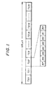
- FIG.1 is a diagram showing a transmission format of 2.048 Mbps.
- TS0 denotes a frame synchronizing time slot
- TS1 through TS14 denote bearer data time slots
- TS15 and TS16 denote bearer data time slots or communication channel time slots
- TS17 through TS30 denote bearer data time slots
- TS31 denotes bearer data time slot or communication channel time slot.
- LAP-V5 which is based on the ISDN LAP-D protocol is used as the message format.
- the ISDN D-channel frame is also converted into the same frame format as the LAP-V5 and is transmitted using the same time slot (communication channel).
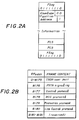
- FIGS.2A and 2B are diagrams for explaining a format of the LAP-V5 frame.
- FIG.2A shows the format of the LAP-V5 frame (V5-envelope frame), and
- FIG.2B shows the relationship of envelope function addresses (EFaddr) and frame contents.
- the LAP-V5 frame is made up of an address field indicating the envelope function address, information indicating data corresponding to the envelope function address, a frame check sequence (FCS) for making error detection with respect to the envelope function address and the information, and flags which are added to the start and end of the LAP-V5 frame.
- the envelope function address is made up of 13 bits and is added with 3 bits of error bits. The error bits indicate a normal state when the bit values are "001" and otherwise indicate an abnormal state.
- the frame contents of the envelope function addresses are user port information which indicates the ISDN D-channel for the addresses 0 to 8175, LAP-V5 protocol information for the addresses 8176 to 8180, and spare for the addresses 8181 through 8191.
- the address 8176 indicates signaling information of a public switched telephone network (PSTN), 8177 indicates a control protocol (connecting information) of the V5 interface, 8178 indicates information of a bearer channel connection (BCC) protocol, 8179 indicates information of a protection protocol, and 8180 indicates information of a link control protocol.
- PSTN public switched telephone network
- BCC bearer channel connection
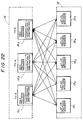
- FIG.3 is a system block diagram showing the construction of a network to which the present invention may be applied as will be described later in the specification.
- the network shown in FIG.3 includes a switched network 1, a V5 exchange which is a local exchange (LE) coupled to the switched network 1, and an access network (AN) 3 which is coupled to the V5 exchange 2 via a transmission path of the V5 interface.
- a switched network 1 a V5 exchange which is a local exchange (LE) coupled to the switched network 1
- AN access network
- the access network 3 includes a V5 interface processor 4 which is provided with the functions of the V5 interface with respect to the V5 exchange 2, a PSTN subscriber interface 5 which connects a plurality of telephone sets 6, an ISDN subscriber interface 7 which connects a plurality of ISDN terminals 8, and a system manager 9 which controls operations of the V5 interface processor 4, the PSTN subscriber interface 5 and the ISDN subscriber interface 7.
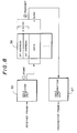
- FIG.4 is a system block diagram for explaining the operation of the network shown in FIG.3 when the PSTN is in use.
- the V5 exchange 2 includes a system manager 10 for controlling the operation of the V5 exchange 2. Signal flows are indicated by bold lines in FIG.4.
- audio data from the telephone set 6 are transmitted and received using one of the time slots in the user data channel (TS1 through TS14, TS17 through TS30) of the V5 interface.
- Hook information (on-hook, off-hook) and dial pulse information from the telephone set 6 are converted into the V5 message format in the system manager 9 of the access network 3.
- the converted information is exchanged between the system manager 9 of the access network 3 and the system manager 10 of the V5 exchange 2 using one of the time slots in the communication channel (TS15, TS16, TS31) of the V5 interface.
- FIG.5 is a system block diagram for explaining the operation of the network shown in FIG.3 when the ISDN is in use.
- those parts which are the same as those corresponding parts in FIG.3 are designated by the same reference numerals.
- Signal flows are indicated by bold lines in FIG.5.
- B-channel data from the ISDN terminal 8 are transmitted and received using two time slots in the user data channel (TS1 through TS14, TS17 through TS30) of the V5 interface.
- D-channel data from the ISDN terminal 8 are added with the envelope function address and converted into an ISDN frame relay format of the V5 interface in the system manager 9 of the access network 3.
- the converted data are exchanged between the system manager 9 of the access network 3 and the system manager 10 of the V5 exchange 2 using one of the time slots in the communication channel (TS15, TS16, TS31) of the V5 interface.
- V5 interface processor 4 In order to reduce the size of the access network 3 shown in FIG.3, it is desirable to realize the V5 interface processor 4 in the form of a 1-chip LSI. But conventionally, various problems prevented the realization of the V5 interface functions by a 1-chip LSI.
- the circuit scale of the V5 interface processor 4 becomes extremely large, thereby making it extremely difficult to form the V5 interface processor 4 by a 1-chip LSI.
- the load on the V5 interface processor 4 becomes large, thereby making it difficult for a single processor to carry out the processing.
- Another and more specific object of the present invention is to provide a V5 interface architecture which can realize the functions of the DMAC, the ISDN frame relay and the LAP-V5 protocol in conformance with the V5 interface standard by a 1-chip LSI.
- Still another object of the present invention is to provide a V5 interface architecture connectable via a transmission path to a local exchange which is coupled to a switching network, comprising HDLC (High Level Data Link Control Procedure) protocol manager means for processing a HDLC protocol of a V5 interface, LAP-V5 (Link Access Procedure for V5) protocol manager means for processing a LAP-V5 protocol, ISDN (Integrated Services Digital Network) protocol manager means for processing an ISDN protocol and processing an ISDN frame relay, and DMA (Direct Memory Access) controller means for carrying out a DMA control with respect to data exchanges between external memory means and the HDLC protocol manager means, the LAP-V5 protocol manager means and the ISDN protocol manager means, where the HDLC protocol manager means, the LAP-V5 protocol manager means, the ISDN protocol manager means and the DMA controller means are provided in a single LSI (large scale integrated circuit) chip.
- HDLC High Level Data Link Control Procedure
- LAP-V5 Link Access Procedure for V5 protocol
- ISDN Integrated Services Digital Network
- ISDN
- V5 interface architecture of the present invention it is possible to greatly reduce the circuit scale that is required for the V5 interface control and the V5 protocol control. In addition, it is possible to improve the processing speed of a processing part of the processor, and also reduce the required memory capacity. Moreover, it is possible to realize the V5 interface functions by a 1-chip LSI.
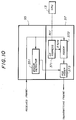
- FIG.6 is a system block diagram for explaining a first embodiment of a V5 interface architecture according to the present invention.
- FIG.6 shows the construction of a V5 LSI which realizes a V5 interface processor.
- a V5 interface control and a V5 protocol process in conformance with the V5 interface standard are realized by a 1-chip LSI.
- a V5 LSI 11 shown in FIG.6 is coupled to a random access memory (RAM) 12, a central processing unit (CPU) 13 and a processor bus 14 which are provided externally to the V5 LSI 11.
- the processor bus 14 is coupled to the CPU 13, and the CPU 13 controls the general operation of the V5 LSI 11.
- high-level data link control procedure (HDLC) frame managers 16 process HDLC protocols.
- the HDLC frame managers 16 that are provided amount to 3 time slots corresponding to the frames which are exchanged with timings of TS15, TS16 and TS31.
- a selector 17 inserts the data which are transmitted from the HDLC frame managers 16 of each of the 3 time slots on a 2.048 Mbps line with timings of TS15, TS16 and TS31.
- LAP-V5 protocol managers 18 process LAP-V5 protocols.
- the LAP-V5 protocol managers 18 that are provided amount to 5 channels corresponding to the envelope function addresses 8176 through 8180, and process the corresponding data in parallel.
- a time slot selector 19 carries out the data transfer between the HDLC frame managers 16 amounting to the 3 time slots and the LAP-V5 protocol managers 18 amounting to the 5 channels.
- An ISDN frame manager 20 processes ISDN protocols.
- a DMAC 21 controls DMA transfer of data between the RAM 12 and the HDLC frame managers 16, the LAP-V5 protocol managers 18 and the ISDN frame manager 20.
- a control register 22 holds command information of the CPU 13.
- a status register 23 holds status information of the CPU 13.
- the V5 LSI 11 shown in FIG.6 is realized by a 1-chip LSI.
- FIG.7 is a system block diagram for explaining second through seventh embodiments of the V5 interface architecture according to the present invention.
- FIG.7 shows the HDLC frame manager 16 for processing the HDLC of the V5 interface, together with LAP-V5 protocol managers 18 1 through 18 5 respectively corresponding to the envelope function addresses n through n+4.
- an envelope function address detector 26 shown in FIG.7 when receiving the communication channel by the V5 interface, separates a V5 envelope frame from the data received by the HDLC protocol managers 16, detects the envelope function address, and determines the block of the LAP-V5 protocol managers 18 amounting to the 5 channels to which block the data are to be transmitted.
- an error frame envelope function non-correspondence detector 27 shown in FIG.7 detects an error frame and an envelope function non-correspondence from the data received by the HDLC protocol managers 16.
- the error frame envelope function non-correspondence detector 27 detects an abnormality of an address field from error bits or, receives a non-supported address
- the error frame envelope function non-correspondence detector 27 carries out a control so as not to send the error frame and the envelope function to the LAP-V5 protocol managers 18.
- the LAP-V5 protocol managers 18 need not detect the error frame and the envelope function non-correspondence. Accordingly, compared to the case where the LAP-V5 protocol managers are provided with such detecting functions, it is possible to reduce the circuit scale of the envelope function non-correspondence detecting function by approximately 1/5.
- a start/end flag deleting unit 28 shown in FIG.7 when receiving the communication channel by the V5 interface, a start/end flag deleting unit 28 shown in FIG.7 simultaneously deletes a start flag and an end flag when separating the V5 envelope frame from the data received by the HDLC protocol managers 16. Thereafter, the start/end flag deleting unit 28 transmits only the data, deleted of the flags, to the LAP-V5 protocol managers 18 according to the envelope function addresses.
- a "0" deleting unit 29 shown in FIG.7 when receiving the communication channel by the V5 interface, deletes predetermined unnecessary “0”s from the data received by the HDLC protocol managers 16. Thereafter, the "0" deleting unit 29 transmits only the data, deleted of the predetermined unnecessary "0”s, to the LAP-V5 protocol managers 18 according to the envelope function addresses.
- the predetermined unnecessary “0”s are introduced according to the provisions of the HDLC protocol.
- "11111” appears in the data
- "0"s are inserted thereafter at the transmitting end, so that a patterns identical to the start flag and the end flag will not appear in the data.
- the original data is restored by deleting the "0"s after the "11111".
- a contention arbitrator 30 shown in FIG.7 when transmitting the data exchanged in a communication path between the plurality of LAP-V5 protocol managers 18 and HDLC protocol managers 16 by multiplexing the data to data of the communication channel, a contention arbitrator 30 shown in FIG.7 carries out a contention arbitration with respect to the transmitting data in the communication path.
- a start/end flag adder 31 shown in FIG.7 adds a start flag and an end flag to the data subjected to the contention arbitration, and transmits the data with the added flags in the format of the V5 envelope frame.
- a "0" inserting unit 32 shown in FIG.7 inserts "0"s to the transmitting data in the communication paths subjected to the contention arbitration based on the provisions of the HDLC protocol, so as to prevent the data from being confused with the start flag and the end flag. Thereafter, the data, inserted with the "0"s, are added with the start flag and the end flag and transmitted in the format of the V5 envelope frame.
- FIG.8 is a system block diagram for explaining eighth and ninth embodiments of the V5 interface architecture according to the present invention.
- FIG.8 shows a method of storing received data in the HDLC protocol managers 16 of the V5 interface.
- a HDLC receiving unit 35 shown in FIG.8 stores only a data portion of the received data into a memory 36.
- a storage region of the memory 36 includes a region amounting to 2 bytes for adding the envelope function address, so that an arbitrary envelope function address may be added.
- FIG.9 is a system block diagram for explaining a conceivable method of adding an envelope function address.
- a HDLC receiving unit 135 receives the data portion of the frame received by a HDLC receiving unit 135 and stores the data in a first memory 141.
- a CPU 139 carries out a process of adding the envelope function address
- the received data are moved to another memory 142 so that the envelope function address is added thereto.
- the data added with the envelope function address and stored in the memory 142 are transmitted via a HDLC transmitting unit 137.
- the eighth embodiment it is unnecessary to carry out the process of moving the received data to another memory as in the conceivable method shown in FIG.9, and the data can be transmitted by simply setting the envelope function address in an empty region of the memory 36. As a result, the ISDN frame relay can be realized at a high speed.
- the envelope function address is preset in the region of the memory 36 for adding the envelope function address in FIG.8.
- the envelope function address is preset in the region of the memory 36 for adding the envelope function address in FIG.8.
- the ISDN frame relay can be realized at a high speed.
- FIG.10 is a system block diagram for explaining tenth and eleventh embodiments of the V5 interface architecture according to the present invention.
- FIG.10 shows a method of storing received data and transmitting the data in the HDLC protocol managers 16 of the V5 interface.
- the HDLC transmitting unit 37 does not store the received data in a memory. Instead, the HDLC transmitting unit 37 inserts a 2-byte envelope function address 371 that is set from a CPU 13 into the frame by an adder 372 and transmits the frame as it is by adding a frame check sequence (FCS) in a FCS adder 373.
- FCS frame check sequence
- the HDLC receiving unit 35 shown in FIG.10 is provided with an error detector 351 for detecting an error frame of the received data.
- the FCS adder 373 inverts the FCS responsive to the detected error frame relative to the normal FCS and transmits the frame by adding the inverted FCS.
- the error frame can be destroyed in the next receiving stage or block, that is, at the LAP-V5 protocol managers 18.
- FIG.11 is a system block diagram for explaining a twelfth embodiment of the V5 interface architecture according to the present invention.
- FIG.11 shows a method of carrying out contention arbitration in the DMAC 21 of the V5 interface.
- each arrow indicated by a solid line indicates a request, and each arrow indicated by a dotted line indicates an acknowledge.
- an arbitrary number of DMA requests are made from the 5 channels of the LAP-V5 protocol managers 18 1 through 18 5 and the 1 channel of the HDLC protocol managers 16.
- n requests are made from the 5 channels of the LAP-V5 protocol managers 18 1 through 18 5
- m requests are made from the 1 channel of the HDLC protocol manager 16.
- the DMAC 21 includes contention arbitrators 211 through 216 for carrying out contention arbitration with respect to the requests from the corresponding LAP-V5 protocol managers 18 1 through 18 5 and HDLC protocol manager 16, and a contention arbitrator 217 for carrying out contention arbitration with respect to results of contention arbitration made in the contention arbitrators 211 through 216, so as to hierarchically carry out the contention arbitration of the requests.
- one request is output from the contention arbitrator 217 so as to make an access to the RAM 12.
- the contention arbitrators 211 through 215 respectively carry out contention arbitration with respect to the n requests from the corresponding LAP-V5 protocol managers 18 1 through 18 5 so as to select 1 request from each of the LAP-V5 protocol managers 18 1 through 18 5
- the contention arbitrator 216 carries out contention arbitration with respect to the m requests from the HDLC protocol manager 16 so as to select 1 request from the HDLC protocol manager 16.
- 6 requests are selected at the input part of the DMAC 21, and the contention arbitrator 217 thereafter selects 1 valid request by carrying out contention arbitration with respect to the 6 requests at the output part of the DMAC 21.
- the DMAC 21 returns 1 acknowledge with respect to the selected valid request, so as to answer a valid acknowledge with respect to the request which is selected at the output part of the DMAC 21 from the 6 requests which are selected at the input part of the DMAC 21. Furthermore, the DMAC 21 returns an acknowledge with respect to each request which is valid as a result of the contention arbitration made at the input part of the DMAC 21.
- the DMAC 21 selects 1 valid request from the arbitrary requests from the 5 channels of the LAP-V5 protocol managers 18 1 through 18 5 and the 1 channel of the HDLC protocol manager 16, and returns 1 valid acknowledge with respect to the selected valid request.
- this embodiment does not carry out the contention arbitration simultaneously with respect to all of the requests, but carries out the contention arbitration in divisions by employing a tree structure, so as to hierarchically reduce the selected requests. As a result, it is possible to carry out the contention arbitration at a high speed compared to the case where the contention arbitration is carried out simultaneously with respect to all of the requests.
- FIG.12 is a timing chart for explaining a thirteenth embodiment of the V5 interface architecture according to the present invention.
- the timing chart of FIG.12 shows access timings of the DMAC 21 when making an access to the RAM 12.
- the DMAC 21 when making an access to the RAM 12 so as to make a read/write in the V5 interface, the DMAC 21 makes a polling with respect to the requests selected as in the case of the twelfth embodiment described above.
- the polling is made at timings indicated by dotted arrows in FIG.12 within the DMA timing.
- the DMAC 21 judges whether the DMA is to continue or to end based on the state of the request, and controls the DMA depending on the judgement.
- the requests selected as in the case of the twelfth embodiment includes, a command request, a status request, a command header clear request, a frame retransmission request and a frame transmission request.
- the access to the RAM 12, that is, the read/write is carried out based on a CPU clock (CPU CLK), so that 4 CPU clocks (CPU CLK) correspond to 1 read/write cycle.
- CPU CLK CPU clock
- 1 read/write cycle may correspond to an arbitrary number of CPU clocks (CPU CLK) other than 4.
- the read/write timing determines data (DATA) and address (ADDRESS) at rising edges of a data strobe signal (XUDS/XLDS) and an address strobe signal (XAS).
- DATA data
- ADRESS address strobe signal
- XUDS/XLDS data strobe signal
- XAS address strobe signal
- FIG.13 is a system block diagram for explaining a fourteenth embodiment of the V5 interface architecture according to the present invention.
- FIG.13 shows a contention arbitration method of the DMA controller 21.
- each arrow indicated by a solid line indicates a request, and each arrow indicated by a dotted line indicates an acknowledge.
- an arbitrary number of DMA requests are made from the 5 channels of the LAP-V5 protocol managers 18 and the 1 channel of the HDLC protocol managers 16.
- n requests are made from the 5 channels of the LAP-V5 protocol managers 18, and m requests are made from the 1 channel of the HDLC protocol manager 16.
- the DMAC 21 finally selects 1 request by making contention arbitration with respect to the requests, and makes an access to the RAM 12.
- the DMAC 21 includes a contention arbitrator 21a for carrying out contention arbitration with respect to a plurality of write requests to select 1 write request, a contention arbitrator 21b for carrying out contention arbitration with respect to a plurality of read requests to select 1 read request, and a read/write contention arbitrator 21c for carrying out contention arbitration with respect to the 1 write request and 1 read request, so as to select 1 write/read request.
- the write/read contention arbitrator 21c distinguishes a write mode and a read mode depending on a write/read state signal which indicates the write or read mode.
- FIG.13 shows only the circuit construction of the DMAC 21 with respect to the requests from one block out of the 5 channels of LAP-V5 protocol managers 18 and the 1 channel of HDLC protocol manager 16.
- FIGS.14 and 15 respectively are diagrams for explaining a fifteenth embodiment of the V5 interface architecture according to the present invention.
- FIG.14 is a system block diagram showing a part of the HDLC protocol manager 16
- FIG.15 is a diagram showing the relationship of the envelope function address and binary data. In this embodiment, it is possible to identify the envelope function addresses allocated in the V5 interface by setting only the lower 4 bits.
- the envelope function addresses allocated in the V5 interface are 8176 through 8180 in decimal.
- the upper 9 bits of the envelope function addresses are the same, and only the lower 4 bits differ depending on the envelope function address, as shown in FIG.15. In this embodiment, only 5 addresses need to be identified, and for this reason, it is possible to identify the envelope function addresses by setting only the lower 4 bits.
- the CPU 13 sets the lower 4 bits of the envelope function address in an envelope function address setting unit 41 which comprises a register.
- An envelope function address state manager 42 identifies the envelope function address from the upper 9 bits of the envelope function address which are fixedly set, and the lower 4 bits of the envelope function address set in the envelope function address setting unit 41.
- this embodiment can reduce the circuit scale of the envelope function address setting unit 43 by approximately 1/3 because only 4 bits of data need to be held.
- regions of the RAM 12 in the V5 interface are fixed regardless of the envelope function address.
- the upper bits of the address of the RAM 12 may be treated as fixed values. Hence, it is possible to reduce the circuit scale of a latch circuit which would be necessary to if the upper bits of the address were to be held by the latch circuit.
- FIG.16 is a system block diagram for explaining a seventeenth embodiment of the V5 interface architecture according to the present invention.
- FIG.16 shows a method of making an access to a state transition table when carrying out a process in conformance with the LAP-V5 protocol procedure in the V5 interface.
- a receiving unit 143 receives the LAP-V5 frame and makes a state detection. Then, an operation process state corresponding to the detected state is read from a state transition table 144, so as to recognize the next operation to be carried out.
- a transmitting unit 145 transmits the LAP-V5 frame based on the recognized operation to be carried out.
- the state transition table 144 is provided within the V5 LSI 11. Hence, compared to the case where the state transition is managed by an external read only memory (ROM) or the like, this embodiment can control the LAP-V5 protocol by hardware without having to rely on software control of a processor.
- ROM read only memory
- FIG.17 is a system block diagram for explaining an eighteenth embodiment of the V5 interface architecture according to the present invention.
- FIG.17 shows a method of making an access to a state transition table when carrying out a process in conformance with the LAP-V5 protocol in the V5 interface.
- the state transition table 144 of the seventeenth embodiment described above is managed by hardware. More particularly, when an arbitrary state is generated and an access is to be made to the state transition table 144 shown in FIG.16, a state detector 146 receives the LAP-V5 frame and makes a state detection. In FIG.17, an access number determination unit 148 recognizes a number of accesses to be made depending on the state detected by the state detector 146. An address generator 147 generates a table access based on the state detected by the state detector 146 and an access signal from the access number determination unit 148 indicative of the number of accesses to be made. The access to the state transition table 144 is made based on the table address generated by the address generator 147 and the access signal from the access number determination unit 148.
- FIG.18 is a diagram for explaining a nineteenth embodiment of the V5 interface architecture according to the present invention.
- FIG.18 shows a method of forming a state transition table when carrying out a process in conformance with the LAP-V5 protocol procedure in the V5 interface.
- the number of accesses differs depending on the state. For this reason, when a fixed region is secured for the number of accesses, the region is not efficiently utilized and may be wasted because the number of accesses may actually not require all of the region.
- the region of the state transition table 144 is set as shown in FIG.18 when employing the seventeenth and eighteenth embodiment described above.
- states 1, 2, 3, 4, ... are set by filling the region of the state transition table 144 in the generated order.
- FIGS.19A and 19B respectively are diagrams for explaining a twentieth embodiment of the V5 interface architecture according to the present invention.
- FIG.19B shows a method of making an access to a state transition table in this embodiment when carrying out a process in conformance with the LAP-V5 protocol in the V5 interface
- FIG.19A shows a normal method of making the access to the state transition table for comparison purposes.
- the 2 actions (A) and (B) are reduced into 1 action (A, B), so that only 1 access is required to the state transition table 144 as shown in FIG.19B. Therefore, according to this embodiment, it is possible to reduce the number of accesses to be made to the state transition table 144.
- FIG.20 is a system block diagram for explaining a twenty-first embodiment of the V5 interface architecture according to the present invention.
- FIG.20 shows a method of reading a state transition table when carrying out a process in conformance with the LAP-V5 protocol in the V5 interface.
- all patterns of the actions with respect to the existing states are coded in the state transition table 144 shown in FIG.20 which is similar to that of the seventeenth embodiment described above except that all patterns of the actions are coded.
- the code of the action read from the state transition table 144 is decoded in a decoder 149 so as to determine the action.
- this embodiment can reduce the number of accesses made to the state transition table 144 and reduce the region of the state transition table 144.
- FIG.21 is a system block diagram for explaining a twenty-second embodiment of the V5 interface architecture according to the present invention.
- FIG.21 shows a method of making an access to a state transition table when carrying out a process in conformance with the LAP-V5 protocol using a plurality of communication paths in the V5 interface.
- a contention arbitrator 50 carries out contention arbitration with respect to the accesses from the 5 channels of the LAP-V5 protocol managers 18, so as to control the plurality of communication paths by a single state transition table 144.
- FIG.22 is a system block diagram for explaining a twenty-third embodiment of the V5 interface architecture according to the present invention.
- FIG.22 shows a method of controlling communication paths when carrying out a process in conformance with the LAP-V5 protocol using the plurality of communication paths in the V5 interface.
- This embodiment can control the plurality of communication channels by the transmission frame generators only amounting to the communication channels.
- the present invention it is possible to greatly reduce the circuit scale that is required for the V5 interface control and the V5 protocol control. In addition, it is possible to improve the processing speed of a processing part of the processor, and also reduce the required memory capacity. Moreover, it is possible to realize the V5 interface functions by a 1-chip LSI.
Landscapes
- Engineering & Computer Science (AREA)
- Computer Networks & Wireless Communication (AREA)
- Communication Control (AREA)
- Use Of Switch Circuits For Exchanges And Methods Of Control Of Multiplex Exchanges (AREA)
- Telephonic Communication Services (AREA)
- Data Exchanges In Wide-Area Networks (AREA)
- Interface Circuits In Exchanges (AREA)
Applications Claiming Priority (2)
| Application Number | Priority Date | Filing Date | Title |
|---|---|---|---|
| JP33407/96 | 1996-02-21 | ||
| JP8033407A JPH09233181A (ja) | 1996-02-21 | 1996-02-21 | V5インタフェースの構成方式 |
Publications (1)
| Publication Number | Publication Date |
|---|---|
| EP0792079A1 true EP0792079A1 (fr) | 1997-08-27 |
Family
ID=12385753
Family Applications (1)
| Application Number | Title | Priority Date | Filing Date |
|---|---|---|---|
| EP96113533A Withdrawn EP0792079A1 (fr) | 1996-02-21 | 1996-08-23 | Architecture d'interface V5 |
Country Status (2)
| Country | Link |
|---|---|
| EP (1) | EP0792079A1 (fr) |
| JP (1) | JPH09233181A (fr) |
Cited By (11)
| Publication number | Priority date | Publication date | Assignee | Title |
|---|---|---|---|---|
| WO1998018267A1 (fr) * | 1996-10-17 | 1998-04-30 | Nokia Telecommunications Oy | Procedure pour explorer ou deconnecter une ligne de module dans un noeud d'acces v5.2 |
| WO1999065187A3 (fr) * | 1998-06-12 | 2000-03-16 | Ericsson Telefon Ab L M | Gestion de reseau |
| WO2000030371A3 (fr) * | 1998-11-17 | 2000-08-10 | Nokia Networks Oy | Procede et systeme de gestion d'une interface v5 |
| US6278688B1 (en) * | 1997-03-18 | 2001-08-21 | Nokia Telecommunications Oy | Procedure for ensuring the operation of signalling channels in a V5 interface |
| EP0903956A3 (fr) * | 1997-08-21 | 2002-01-02 | Fujitsu Limited | Un réseau entre un central et un réseau d'accès, et un circuit semi-conducteur intégré à grande échelle pour utilisation dans le réseau |
| KR100328435B1 (ko) * | 1999-12-29 | 2002-03-16 | 박종섭 | 브이5.2 계층3 처리 장치와 호제어 프로세서 간 메시지라우팅 방법 |
| KR100328436B1 (ko) * | 1999-12-29 | 2002-03-16 | 박종섭 | 브이5.2 계층3 처리 장치와 호제어 프로세서 간 메시지정합 기능의 부하분담 방법 |
| US6535508B1 (en) * | 1997-09-25 | 2003-03-18 | Nec Corporation | Multiple connection method and device for subscriber access network |
| US6647018B1 (en) * | 1997-12-17 | 2003-11-11 | Nokia Corporation | Method for implementing ISDN user port status monitoring |
| US6762998B1 (en) * | 1999-06-18 | 2004-07-13 | Fujitsu Limited | Access network system |
| CN115766916A (zh) * | 2022-10-27 | 2023-03-07 | 山东云海国创云计算装备产业创新中心有限公司 | 通过spi模拟hdlc协议的编解码方法、系统、终端及存储介质 |
Families Citing this family (2)
| Publication number | Priority date | Publication date | Assignee | Title |
|---|---|---|---|---|
| KR100334906B1 (ko) * | 1999-12-27 | 2002-05-04 | 오길록 | 브이5 시스템에서의 멀티 태스크 구성 방법 |
| KR100425985B1 (ko) * | 1999-12-28 | 2004-04-03 | 엘지전자 주식회사 | 교환 시스템에서 디 채널 패킷 데이터 처리장치 |
Citations (4)
| Publication number | Priority date | Publication date | Assignee | Title |
|---|---|---|---|---|
| EP0016426A1 (fr) * | 1979-03-15 | 1980-10-01 | CSELT Centro Studi e Laboratori Telecomunicazioni S.p.A. | Central téléphonique digital |
| US4949338A (en) * | 1987-04-06 | 1990-08-14 | Racal Data Communications Inc. | Arbitration in multiprocessor communication node |
| US5274634A (en) * | 1991-09-30 | 1993-12-28 | Mitel Corporation | PABX common channel relay system |
| US5446731A (en) * | 1992-11-26 | 1995-08-29 | Samsung Electronics Co., Ltd. | Signaling channel data transmitting/receiving circuit of a primary multiplexer |
-
1996
- 1996-02-21 JP JP8033407A patent/JPH09233181A/ja not_active Withdrawn
- 1996-08-23 EP EP96113533A patent/EP0792079A1/fr not_active Withdrawn
Patent Citations (4)
| Publication number | Priority date | Publication date | Assignee | Title |
|---|---|---|---|---|
| EP0016426A1 (fr) * | 1979-03-15 | 1980-10-01 | CSELT Centro Studi e Laboratori Telecomunicazioni S.p.A. | Central téléphonique digital |
| US4949338A (en) * | 1987-04-06 | 1990-08-14 | Racal Data Communications Inc. | Arbitration in multiprocessor communication node |
| US5274634A (en) * | 1991-09-30 | 1993-12-28 | Mitel Corporation | PABX common channel relay system |
| US5446731A (en) * | 1992-11-26 | 1995-08-29 | Samsung Electronics Co., Ltd. | Signaling channel data transmitting/receiving circuit of a primary multiplexer |
Non-Patent Citations (5)
| Title |
|---|
| "METHOD FOR CONVERTING TDM DATA INTO PACKETS FOR TRANSPORT IN A FAST-PACKET SWITCH", IBM TECHNICAL DISCLOSURE BULLETIN, vol. 35, no. 4A, 1 September 1992 (1992-09-01), pages 123 - 131, XP000314706 * |
| GILLESPIE A: "INTERFACING ACCESS NETWORKS TO EXCHANGES: THE ETSI V5 APPROACH", GLOBECOM '92, "COMMUNICATION FOR GLOBAL USERS", vol. 3 OF 3, 6 December 1992 (1992-12-06) - 9 December 1992 (1992-12-09), ORLANDO, FLORIDA, pages 1754 - 1758, XP000390475 * |
| JAMES K ET AL: "TOWARDS A GLOBAL V5 INTERFACE", PROCEEDINGS OF THE INTERNATIONAL CONFERENCE ON COMMUNICATIONS (ICC '93), vol. 2 OF 3, 23 May 1993 (1993-05-23) - 26 May 1993 (1993-05-26), GENEVA, pages 873 - 877, XP000371206 * |
| THEEUWS R ET AL: "IMPLEMENTATION OF ISDN IN THE OMNI", INTERNATIONAL SWITCHING SYMPOSIUM (ISS), vol. 3, 25 October 1976 (1976-10-25) - 29 October 1976 (1976-10-29), PHOENIX, ARIZONA, pages 557 - 563, XP002032402 * |
| YOSHIDA Y ET AL: "VLSI DESIGN IN ISDN PROTOCOL HANDLER", IEEE/IEICE GLOBAL TELECOMMUNICATIONS CONFERENCE 1987, vol. 3 OF 3, 15 November 1987 (1987-11-15) - 18 November 1987 (1987-11-18), TOKYO, JAPAN, pages 1752 - 1756, XP000012664 * |
Cited By (15)
| Publication number | Priority date | Publication date | Assignee | Title |
|---|---|---|---|---|
| US6711175B1 (en) | 1996-10-17 | 2004-03-23 | Nokia Corporation | Procedure for scanning or disconnecting a module line in a V5.2 access node |
| WO1998018267A1 (fr) * | 1996-10-17 | 1998-04-30 | Nokia Telecommunications Oy | Procedure pour explorer ou deconnecter une ligne de module dans un noeud d'acces v5.2 |
| USRE40451E1 (en) | 1997-03-18 | 2008-08-05 | Nokia Corporation | Procedure for ensuring the operation of signalling channels in a V5 interface |
| US6278688B1 (en) * | 1997-03-18 | 2001-08-21 | Nokia Telecommunications Oy | Procedure for ensuring the operation of signalling channels in a V5 interface |
| EP0903956A3 (fr) * | 1997-08-21 | 2002-01-02 | Fujitsu Limited | Un réseau entre un central et un réseau d'accès, et un circuit semi-conducteur intégré à grande échelle pour utilisation dans le réseau |
| US6535508B1 (en) * | 1997-09-25 | 2003-03-18 | Nec Corporation | Multiple connection method and device for subscriber access network |
| US6647018B1 (en) * | 1997-12-17 | 2003-11-11 | Nokia Corporation | Method for implementing ISDN user port status monitoring |
| WO1999065187A3 (fr) * | 1998-06-12 | 2000-03-16 | Ericsson Telefon Ab L M | Gestion de reseau |
| US6631189B2 (en) | 1998-11-17 | 2003-10-07 | Nokia Corporation | Method and system for the management of a V5 interface |
| WO2000030371A3 (fr) * | 1998-11-17 | 2000-08-10 | Nokia Networks Oy | Procede et systeme de gestion d'une interface v5 |
| US6762998B1 (en) * | 1999-06-18 | 2004-07-13 | Fujitsu Limited | Access network system |
| EP1061765A3 (fr) * | 1999-06-18 | 2006-08-09 | Fujitsu Limited | Système de gestion d'un réseau d'accès |
| KR100328436B1 (ko) * | 1999-12-29 | 2002-03-16 | 박종섭 | 브이5.2 계층3 처리 장치와 호제어 프로세서 간 메시지정합 기능의 부하분담 방법 |
| KR100328435B1 (ko) * | 1999-12-29 | 2002-03-16 | 박종섭 | 브이5.2 계층3 처리 장치와 호제어 프로세서 간 메시지라우팅 방법 |
| CN115766916A (zh) * | 2022-10-27 | 2023-03-07 | 山东云海国创云计算装备产业创新中心有限公司 | 通过spi模拟hdlc协议的编解码方法、系统、终端及存储介质 |
Also Published As
| Publication number | Publication date |
|---|---|
| JPH09233181A (ja) | 1997-09-05 |
Similar Documents
| Publication | Publication Date | Title |
|---|---|---|
| EP0488685B1 (fr) | Circuit d'interface RNIS | |
| USH586H (en) | ISDN D channel handler | |
| US5541930A (en) | Byte aligned communication system for transferring data from one memory to another memory over an ISDN | |
| US5048012A (en) | Data link controller with flexible multiplexer | |
| EP0792079A1 (fr) | Architecture d'interface V5 | |
| US5058111A (en) | Subscriber line interface circuit in a switching system | |
| JP2794672B2 (ja) | ディジタル通信網へデータ通信装置を接続するための装置 | |
| JP2815304B2 (ja) | 複数の独立したディジタル通信チャネルを介して高速度ディジタル・データ・フローを送信する方法 | |
| US5056084A (en) | System for transmitting hdlc frames on a pcm type link using a single hdlc circuit and a transposition buffer memory | |
| EP0079426B1 (fr) | Système de communication de données | |
| US6009093A (en) | Apparatus and method for interfacing private exchange to integrated services digital network | |
| US5371740A (en) | Method for data transmission over an internal bus of a workstation, apparatus with an internal bus for implementing the method, and an adapter circuit for the internal bus | |
| US4805171A (en) | Unitary PCM rate converter and multiframe buffer | |
| US4774704A (en) | Interface circuit for connecting a digital equipment to a time multiplex link | |
| US5289465A (en) | Method for data transmission over an internal bus of a workstation apparatus with an internal bus for implementing the method, and an adapter circuit for the internal bus | |
| US5467350A (en) | Conversion of ISDN LAPB and ISDN LAPD frames | |
| US5579300A (en) | Private automatic branch exchange for integrated services digital network | |
| EP0695061A1 (fr) | Procédé d'allocation de canal pour un réseau en anneau | |
| EP0405041B1 (fr) | Interface de terminal ayant un récepteur pour de multiples canaux de communication HDLC servant au traitement de trames de gestion de réseau | |
| JPS63266564A (ja) | ビット向けプロトコルデータ制御器 | |
| JP3586520B2 (ja) | ディジタルメッセージ中継システム | |
| US5517490A (en) | Telecommunication terminal operating at alternative data throughput rates | |
| JP3058138B2 (ja) | 通信端末装置 | |
| KR100226588B1 (ko) | 통신 시스템의 동작 모드 판단 방법 | |
| EP0285331A2 (fr) | Dispositif de commande d'une voie de données |
Legal Events
| Date | Code | Title | Description |
|---|---|---|---|
| PUAI | Public reference made under article 153(3) epc to a published international application that has entered the european phase |
Free format text: ORIGINAL CODE: 0009012 |
|
| AK | Designated contracting states |
Kind code of ref document: A1 Designated state(s): DE GB |
|
| 17P | Request for examination filed |
Effective date: 19971010 |
|
| 17Q | First examination report despatched |
Effective date: 20071015 |
|
| GRAP | Despatch of communication of intention to grant a patent |
Free format text: ORIGINAL CODE: EPIDOSNIGR1 |
|
| STAA | Information on the status of an ep patent application or granted ep patent |
Free format text: STATUS: THE APPLICATION IS DEEMED TO BE WITHDRAWN |
|
| 18D | Application deemed to be withdrawn |
Effective date: 20091030 |