EP0792507B1 - Circuits, systemes et methodes permettant de determination des cellules defectueuses dans une memoire - Google Patents
Circuits, systemes et methodes permettant de determination des cellules defectueuses dans une memoire Download PDFInfo
- Publication number
- EP0792507B1 EP0792507B1 EP95939746A EP95939746A EP0792507B1 EP 0792507 B1 EP0792507 B1 EP 0792507B1 EP 95939746 A EP95939746 A EP 95939746A EP 95939746 A EP95939746 A EP 95939746A EP 0792507 B1 EP0792507 B1 EP 0792507B1
- Authority
- EP
- European Patent Office
- Prior art keywords
- address
- memory
- array
- cell
- row
- Prior art date
- Legal status (The legal status is an assumption and is not a legal conclusion. Google has not performed a legal analysis and makes no representation as to the accuracy of the status listed.)
- Expired - Lifetime
Links
- 230000002950 deficient Effects 0.000 title claims description 44
- 238000000034 method Methods 0.000 title claims description 22
- 239000000872 buffer Substances 0.000 claims description 33
- 238000012360 testing method Methods 0.000 claims description 27
- 238000012545 processing Methods 0.000 claims description 21
- 230000004044 response Effects 0.000 claims description 7
- 230000008569 process Effects 0.000 description 6
- 238000004519 manufacturing process Methods 0.000 description 5
- 230000007547 defect Effects 0.000 description 4
- 238000013461 design Methods 0.000 description 4
- 238000010586 diagram Methods 0.000 description 4
- 230000001747 exhibiting effect Effects 0.000 description 2
- 230000006870 function Effects 0.000 description 2
- 238000006467 substitution reaction Methods 0.000 description 2
- 230000004075 alteration Effects 0.000 description 1
- 238000007664 blowing Methods 0.000 description 1
- 239000007853 buffer solution Substances 0.000 description 1
- 238000010276 construction Methods 0.000 description 1
- 230000001419 dependent effect Effects 0.000 description 1
- 238000005516 engineering process Methods 0.000 description 1
- 239000004973 liquid crystal related substance Substances 0.000 description 1
- 238000012423 maintenance Methods 0.000 description 1
- 230000008439 repair process Effects 0.000 description 1
- 239000004065 semiconductor Substances 0.000 description 1
- 230000003068 static effect Effects 0.000 description 1
- 238000012546 transfer Methods 0.000 description 1
- 238000013519 translation Methods 0.000 description 1
- 230000000007 visual effect Effects 0.000 description 1
Images


Classifications
-
- G—PHYSICS
- G11—INFORMATION STORAGE
- G11C—STATIC STORES
- G11C11/00—Digital stores characterised by the use of particular electric or magnetic storage elements; Storage elements therefor
- G11C11/21—Digital stores characterised by the use of particular electric or magnetic storage elements; Storage elements therefor using electric elements
- G11C11/34—Digital stores characterised by the use of particular electric or magnetic storage elements; Storage elements therefor using electric elements using semiconductor devices
- G11C11/40—Digital stores characterised by the use of particular electric or magnetic storage elements; Storage elements therefor using electric elements using semiconductor devices using transistors
- G11C11/401—Digital stores characterised by the use of particular electric or magnetic storage elements; Storage elements therefor using electric elements using semiconductor devices using transistors forming cells needing refreshing or charge regeneration, i.e. dynamic cells
- G11C11/4063—Auxiliary circuits, e.g. for addressing, decoding, driving, writing, sensing or timing
- G11C11/407—Auxiliary circuits, e.g. for addressing, decoding, driving, writing, sensing or timing for memory cells of the field-effect type
-
- G—PHYSICS
- G11—INFORMATION STORAGE
- G11C—STATIC STORES
- G11C29/00—Checking stores for correct operation ; Subsequent repair; Testing stores during standby or offline operation
- G11C29/70—Masking faults in memories by using spares or by reconfiguring
- G11C29/76—Masking faults in memories by using spares or by reconfiguring using address translation or modifications
-
- G—PHYSICS
- G11—INFORMATION STORAGE
- G11C—STATIC STORES
- G11C29/00—Checking stores for correct operation ; Subsequent repair; Testing stores during standby or offline operation
- G11C29/04—Detection or location of defective memory elements, e.g. cell constructio details, timing of test signals
- G11C29/08—Functional testing, e.g. testing during refresh, power-on self testing [POST] or distributed testing
- G11C29/12—Built-in arrangements for testing, e.g. built-in self testing [BIST] or interconnection details
- G11C29/18—Address generation devices; Devices for accessing memories, e.g. details of addressing circuits
- G11C29/24—Accessing extra cells, e.g. dummy cells or redundant cells
-
- G—PHYSICS
- G11—INFORMATION STORAGE
- G11C—STATIC STORES
- G11C29/00—Checking stores for correct operation ; Subsequent repair; Testing stores during standby or offline operation
- G11C29/70—Masking faults in memories by using spares or by reconfiguring
- G11C29/88—Masking faults in memories by using spares or by reconfiguring with partially good memories
Definitions
- the present invention relates in general to data processing systems and in particular to circuits, systems and methods for accounting for defective cells in a memory device.
- Integrated yield becomes a particular concern when the blocks of circuitry being integrated are of different yielding designs and/or must be fabricated under different process rules. Since the integrated yield of a particular integrated circuit is a function of each of the non-integrated yields (i.e., the respective yields of each of the various types of circuitry blocks), it becomes important to maximize the yield of each type of circuitry being fabricated on the chip.
- DRAM dynamic random access memory
- One way to increase the overall yield of integrated circuits including both logic circuitry and DRAM circuitry is to increase the yield of the DRAM circuitry by "repairing" defective memory cells in the DRAM cell array.
- a DRAM memory device has as many as 10% more "extra" rows of memory cells than specified.
- a wafer test is performed to identify any rows which contain any defective cells. Any rows which are found to contain at least one defective cell are then "replaced” with an operative row taken from the extra rows in the array. This replacement may be performed for example by blowing fuses or otherwise physically altering the circuitry.
- This technique disadvantageously requires several production steps, including the time consuming steps of testing each cell array and replacing the bad rows with good rows by physically altering the chip.
- EP-A2-0 242 854 a data processing system with an array of memory cells as well as a method for working around defective cells in an array of memory cells has come to be known.
- defect relieving technology which replaces defective memory cells of a semiconductor memory device with spare memory cells, use is made of an associative memory. Address information of a defective memory cell is stored as a reference data of the associative memory, and new address information of a spare memory cell is written down as output data of the associative memory.
- the preamble of claim 1 is based on this document.
- circuits and methods which allow for increased yields of DRAM devices.
- circuits and methods would increase integrated yields for integrated circuits including both logic and DRAM circuitry by increasing the yield of the DRAM memory array.
- circuits and methods would help eliminate the time and expense currently required to physically alter the chip to replace bad rows of cells with good rows of cells.
- an associative memory system is used to "work around" bad rows and/or columns of cells in a memory cell array. For example, when an address is generated which calls for the access of a defective row of cells in a memory cell array, that address is translated to an address corresponding to a operative row of cells in the array. In a similar fashion, defective columns of cells in the memory array can be effectively "substituted” by directing any request to access such defective columns to operative columns in the same array.
- the associative memory is formed on the same integrated circuit as the memory array along with circuitry for testing the array for the existence of defective cells and programming circuitry to program the associative memory.
- a data processing system which includes an array of memory cells arranged in rows and columns, each row addressable by an address.
- Address generation circuitry is provided for generating addresses for accessing corresponding rows.
- An associative memory is coupled to the address generation circuitry for translating a first address, received from the address generation circuitry and addressing a defective one of the rows, into a second address addressing an operative one of the rows, the second address being sent to the memory.
- a data processing system which includes a controller for having address generation circuitry for generating addresses to access an associated memory.
- a memory system is provided which includes an array of memory cells arranged in rows and columns and decoding circuitry for selecting ones of the rows and columns in response to received ones of the addresses.
- the data processing system further includes associative memory circuitry operable to translate addresses received from the controller and addressing defective ones of the rows in a first space in the array into addresses addressing corresponding operative ones of the rows in a second space of the array.
- a processing system which includes a memory having an array of memory cells arranged in rows and columns, each column addressable by a column address. Address generation circuitry is also included for generating ones of the addresses for accessing corresponding selected ones of the columns. An associative memory is coupled to the address generation circuitry for translating a first address, received from the address generation circuitry and addressing a defective one of the columns, into a second address addressing an operative ones of the columns, the second address being presented to the memory.
- the principles of the present invention are also related to methods for working around defective rows of cells in an array of memory cells arranged in rows and columns.
- an associative memory is programmed. A first row in the array of the memory is addressed and tested to determine that the first row contains at least one defective cell. A second address is generated for addressing a second row in the array. The first and second addresses are then stored in the associative memory such that the second address is output from the associative memory upon the input of the first address. The first address is then presented to the associative memory such that the second address is output therefrom to address the memory array. The second row of the memory array is then tested to ensure that the second row is operative. Next, an address is input to the associative memory to access at least one cell of a selected row of the array. If the address to the selected row matches an address to a defective row in the array, the address of a corresponding operative row is output to the memory array.
- an associative memory is programmed. Among other things, a first column in the memory array is addressed with a first address. That first address is tested to determine that the first column contains at least one defective cell. A second address is generated for addressing a second column in the array. The first and second addresses are then stored in the associative memory such that upon the input to the associative memory of the firsT address, the second address is output. The first address is then presented to the associative memory such that the second address is output to allow access to the second column in the array. The second column is then tested to ensure that the second column is operative.
- an address to the associative memory can then be input to access at least one cell of a selected column of the array. Then, if the address to the selected column matches an address to a defective column in the array, the address of a corresponding operative row is output from the associative memory to the memory array.
- the embodiments of the present invention provide substantial advantages over the existing an.
- the circuits, systems and methods of the present invention eliminate the need for expensive and time consuming physical alteration of an array of memory cells in order to replace defective rows and columns of cells. Further, the testing efficiency of an array of cells is increased since all testing is done on chip. Additionally, when the principles of the present invention are applied to devices integrating both memory circuitry and logic circuitry on a single chip, the integrated yield for the chip can be substantially increased.
- the principles of the present invention may be applied to provide sufficient functional memory to allow the overall device to be usable, even if the memory is not completely defect free. For example, if 50% functionality of the memory can be achieved the overall device may be usable in a reduced configuration or if 90% functionality of the memory can be achieved, the overall device may fully usable. Finally, since preferably the memory array is tested with each power up of the chip, the integrity of the memory array can be maintained, even if defective cells occur well after fabrication.
- FIGS 1-4 of the drawings in which like numbers designate like parts.
- FIGS 1-4 of the drawings in which like numbers designate like parts.
- FIGS 1-4 of the drawings in which like numbers designate like parts.
- block transfer circuits, systems and methods according to these principles may be employed in any one of a number of processing applications.
- FIGURE 1 is a high level functional block diagram of the portion of a processing system 100 controlling the display of graphics and/or video data.
- System 100 includes a central processing unit 101, a system bus 102, a display controller 103, a frame buffer 104, a digital-to-analog converter (DAC) 105 and a display device 106.
- DAC digital-to-analog converter
- CPU 101 controls the overall operation of system 100, determines the content of any graphics data to be displayed on display unit 106 under user commands, and performs various data processing functions.
- CPU 101 may be for example a general purpose microprocessor used in commercial personal computers.
- CPU 101 communicates with the remainder of system 100 via system bus 102, which may be for example a local bus, an ISA bus or a PCI bus.
- DAC 105 receives digital data from controller 103 and outputs in response the analog data required to drive display 106.
- DAC 105 may also include a color palette, YUV to RGB format various circuitry, and/or x- and y-zooming circuitry, to name a few options.
- Display 106 may be for example a CRT unit, liquid crystal display, electroluminescent display (ELD), plasma display (PLD), or other type of display device which displays images on a display screen as a plurality of pixels.
- LCD electroluminescent display
- PLD plasma display
- system 100 is a VGA system driving a display screen on display 106 of 640 columns by 480 rows of pixels.
- each pixel will be assumed to be defined by 24-bits of RGB data (i.e., 8-bits each for red, green, and blue).
- the absolute maximum size of the physical memory of frame buffer 104 will be 640 columns by 480 rows by 24-bits per pixel or approximately one megabyte.
- the "visual pixels" on the display screen may or may not exactly map to the storage locations in the physical memory of frame buffer 104, depending on the memory formatting selected.
- all 24-bits of color data defining each pixel may be physically stored in sequential storage locations in physical memory (in which case, all 24-bits could be stored in a given page of a DRAM or VRAM) or may be stored in three different banks or rows of the physical memory of the frame buffer 104.
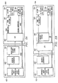
- FIGURE 2A is a more detailed functional block diagram of display controller 103 and frame buffer 104 emphasizing one embodiment of the circuitry implementing the principles of the present invention.
- display controller 103 includes graphics/video controller logic circuitry 201, address generator 202 and an associative memory system 203.
- Frame buffer 104 includes an array of memory cells 204 arranged in M rows and N columns. The rows of array 204 are controlled (selected) by an associated row decoder 205 and the columns of array 204 are coupled to associated column decoder/sense amplifier circuitry 206. Row decoder 205 selects a given row in array 204 during a memory access (read or write) in response to row addresses received through memory input/output circuitry 207.
- column decoders of column decoder/sense amplifier circuitry 206 allow selective access to one or more of the memory cells along a selected row in response to a column address received through input/output circuitry 207.
- Data is exchanged between graphics/video controller logic circuitry 201 and memory array 204 through memory input/output circuitry 207 and column decoder/sense amplifier circuitry 206.
- graphics/video controller logic circuitry 201 may be any one of a number of known controllers modified or programmed, as described below, which control the display of graphics and/or video data.
- graphics/video controller logic circuitry 201 may be implemented by standard VGA controller circuitry.
- address generator 202 may be any one of a number of known address generator designs which generate addresses that allow controller 201 to appropriately access storage locations within memory array 204 via row decoder 205 and column decoder/sense amplifier circuitry 206.
- a memory array 204 is an array of dynamic random access memory (DRAM) cells and the associative memory is implemented in static random access memory (SRAM) cells.
- row decoder 205, column decoder/sense amplifiers 206, and input/output circuitry 207 are of a conventional design.
- associative memory system 203 provides for the "work around" of defective memory cells or groups of defective memory cells within array 204.
- the principles of the present invention in a first embodiment allow for the substitution of an entire row of cells which contains one or more defective cells with another "spare" row of cells which is fully operational.
- a given column in the cell array of a "by one" memory which contains one or more defective cells can be replaced with a "spare" column of cells which contains no defective cells.
- typical DRAM devices include as many as ten percent more rows of cells than specified.
- the entire available storage space of the frame buffer memory (for example, frame buffer 104) is typically required for use as "frame buffer” (often some portion of the remaining "extra” memory space is used for the storage of other types of data required by the CPU and/or display controller).
- a one megabyte frame buffer is typically used in a VGA system displaying data on a display screen as a "display frame" of 640 columns and 480 rows of pixels, each pixel being defined by 24-bits of data for "true color.” Since this system only requires 921,600 bytes of capacity for storing each display frame, approximately ten percent of the one megabyte memory remains unused. With such a substantial amount of extra memory space available, the ability to "work around" defective memory cells or groups of cells becomes theoretically possible. Any "extra" space which can be obtained after the frame buffer space is made available can still be used for other processing operations.
- the "frame buffer space" of array 204 is assigned to the "lower” address space.
- the remaining “upper” row address space is designated for defective cell "work around” purposes.
- the designation of the frame buffer space and the work around space may correspond to different address spaces in array 204.
- the frame buffer space may correspond to the "upper” row address space while the work around space may correspond to the "lower” row address space of array 204.
- the address space of array 107 may be partitioned into frame buffer space and work around space in any of a number of ways.
- controller 201 includes a state machine or microcontroller which tests the rows of cells in the frame buffer space of array 204 and when a defective row is discovered, programs associative memory system 203 to map the address to the defective row in the frame buffer space to the address of an operational row in the work around space. While the testing of array 204 is preferably performed by circuitry within display controller 103, it should be recognized that in alternate embodiments this testing may be performed by test circuitry disposed within frame buffer 103. Hence, when graphics/video controller 201 attempts to access the defective row in the frame buffer space, the corresponding received address is translated by associative memory system 203 and an associated address to an operational row is output to the memory. The actual access is then made to the corresponding operational row in the work around space.
- FIGURE 3 A preferred embodiment of the state machine is described in FIGURE 3.
- the state machine operation starts at step 300 upon the power of display controller 107. Retesting of the memory array 204 and the programming of associative memory system 203 with each power up cycle allow continued maintenance of memory integrity.
- the address of the first row in the frame buffer space of array 204 is loaded into a counter R1. As discussed above, in the preferred embodiment, this address is the lowest address in the address space of array 204 (i.e., address 0).
- the last address to the memory array 204 (including the frame buffer space and the work around space) plus one is loaded into a second counter R2. As discussed above, in the preferred embodiment, the address loaded into counter R2 is the highest address to array 204.
- the associative memory system 203 is reset at step 303 such that an address presented (input) thereto is not translated and is simply passed through.
- Step 304 a test of the cells of the addressed row is initiated.
- Step 304 may be implemented for example by performing a conventional row test in which graphics/video controller 201 writes a pattern of data into the addressed row using row decoder 205 and column decoders 206, reads the pattern back from the addressed row using row decoder 205 and column decoder/sense amplifier circuitry 206, and then compares the data read back with the data originally written in to the address row.
- the row address to array 204 is passed through associative memory system 203, although since no association has been made no translation occurs. If the tested row of the frame buffer space is good then at step 306 the address in counter R1 is incremented.
- a test is performed at step 306 to determine if the end of the available frame buffer space has been reached.
- a comparison is made of the addresses in counters R1 and R2; when the two addresses are equal, the frame buffer space and the work around space have reached each other and no further memory space is available for either purpose. If the end of the available frame buffer space has in fact been reached, then at step 310 the address in counter R1 is decremented and at step 311 testing programming process is complete. If however at step 307 a determination is made that the end of the available frame buffer space has not been reached, then the process continues at step 304 where the new row now addressed by the address in counter R1 is tested for defective cells. The process continues as described above at step 305.
- step 308 the count in counter R2 is decremented (since the initial count loaded into counter R2 is the highest available address plus one, on the initial performance of step 308, the address in counter R2 is decremented to the highest address available to array 204).
- step 309 a test is performed to determine if work around space is available. In the preferred embodiment the counts in R1 and R2 are again compared. If the counts are equal then the available space in memory has been consumed and the processing again proceeds to steps 310 and 311.
- step 312 the associative memory system is programmed to associate the address in counter R1 with the address in counter R2 (i.e., such that the input of the address in R1 results in the output of the address in counter R2).
- the address in counter R1 is again presented to associative memory 203 such that the row addressed by the associated address output from associative memory 203 can itself be tested at step 304.
- the testing continues at step 305 until the address in counter R1 is associated with the address to an operative row in array 204, at which time processing moves to the next row at step 306, or until the entire available memory space has been used at step 311.
- graphics/video controller 201 is ready to process graphics or video data in a conventional manner. Whenever controller 201 (and associated address generator) generates an address which attempts to access a defective row in the frame buffer space of array 204, a match occurs in associative memory system 203 and that address is substituted with the address of the corresponding row in the work around space.
- FIGURE 2B depicts an alternate embodiment of the present invention.
- the associative memory system 203 is implemented within the frame buffer system 104 rather than within display controller 103.
- the circuitry required to test array 204 may be also be disposed within frame buffer 204, for example as part of associative memory system 203 itself.
- the testing of array 204 is performed by circuitry within controller 103, as was discussed above.
- the embodiment of FIGURE 2B has advantages over the embodiment of FIGURE 2A.
- graphics/video controller 201 an address generator 202, must be capable of generating enough address bits to not only address the frame buffer space required for conventional processing operations but also of generating additional address bits to provide access to the work around space of the memory array 204.
- the test circuitry is disposed within associative memory system 203
- the test of memory array 204 is performed and the associative memory programmed without the intervention of the controller 201. Any necessary additional address bits are generated within associative memory. Therefore, controller 201 need only continue to generate the number of row address bits originally required to access the frame buffer space. It should be noted that in this case each address from the controller 201 may map to a longer address word when a work around is being performed.
- a microprocessor or microcontroller operable to perform conventional column and/or row tests is preferably provided within either graphics/video controller 201 in the embodiment of FIGURE 2A or in the associative memory system/memory test circuitry 203 of the embodiment of FIGURE 2B.
- any unused or redundant columns provided in memory array 204 are used to work around bad columns in the frame buffer space by passing each column address through the associative memory system 203.
- the associative memory programming procedure is similar to that of FIGURE 3 and is shown in FIGURE 4.
Landscapes
- Engineering & Computer Science (AREA)
- Microelectronics & Electronic Packaging (AREA)
- Computer Hardware Design (AREA)
- For Increasing The Reliability Of Semiconductor Memories (AREA)
Claims (12)
- Système de traitement de données (100) possédant :caractérisé en ce que :a) une matrice de cellules de mémoire (204) disposées en rangées et en colonnes, chaque dite cellule pouvant être adressée par une adresse,b) un circuit générateur d'adresses (202) servant à produire des adresses parmi lesdites adresses afin de faire accès à des cellules sélectionnées parmi lesdites cellules, etc) une mémoire associative (203) couplée audit circuit générateur d'adresses (202) et servant à transformer une première dite adresse, reçue de la part dudit circuit générateur d'adresses (202) et indiquant une première cellule défectueuse parmi lesdites cellules dans un premier espace de ladite mémoire (204), en une deuxième adresse, ladite deuxième adresse indiquant une deuxième cellule parmi lesdites cellules se trouvant dans un deuxième espace de ladite mémoire (204), ladite deuxième adresse étant envoyée à ladite mémoire (204) ; etd) un circuit de programmation (201) servant à programmer ladite mémoire associative (203) ;
e) ledit circuit de programmation (201) a pour fonction de :ea) présenter la première adresse à la mémoire associative ;eb) adresser la deuxième cellule de la matrice (204) au moyen de la deuxième adresse délivrée par la mémoire associative en réponse à la présentation de la première adresse ; etec) contrôler la deuxième cellule afin d'assurer que la deuxième cellule fonctionne bien. - Système selon la revendication 1, où lesdites première et deuxième adresses comprennent des adresses de rangée.
- Système selon la revendication 1, où lesdites première et deuxième adresses comprennent des adresses de colonne.
- Système selon la revendication 1, 2 ou 3, où ledit circuit générateur d'adresses (202) comprend une partie d'un dispositif de commande (201).
- Système selon la revendication 1, 2, 3 ou 4, où ledit premier espace comprend un espace tampon d'image complète se trouvant à l'intérieur de ladite matrice (204).
- Système selon l'une quelconque des revendications 1, 2, 4 et 5, où ledit circuit de programmation (201, 202) a pour fonction de :adresser une première dite rangée de ladite matrice (204) au moyen de ladite première adresse ; contrôler ladite première rangée afin de déterminer si ladite première rangée contient au moins une dite cellule défectueuse ; produire ladite deuxième adresse ; programmer ladite mémoire associative en vue de la délivrance de ladite deuxième adresse en cas d'application, en entrée, de ladite première adresse ; présenter ladite première adresse audit système de mémoire associative ;adresser une deuxième dite rangée de ladite matrice (204) au moyen de ladite deuxième adresse qui a été délivrée par ladite mémoire associative en réponse à la présentation de ladite première adresse ; etcontrôler ladite deuxième rangée afin d'assurer que ladite deuxième rangée fonctionne bien.
- Système selon l'une quelconque des revendications 1 à 6, où ledit circuit de programmation (201, 202) comprend un automate fini.
- Système selon l'une quelconque des revendications 1 à 7, où ledit circuit de programmation (201, 202) comprend un microrégisseur (201).
- Système selon la revendication 4, où ledit dispositif de commande (201) comprend un dispositif (201) de commande d'affichage.
- Système selon la revendication 4, où ledit dispositif de commande (201) comprend un dispositif (201) de commande VGA.
- Procédé permettant de contourner des cellules défectueuses se trouvant dans une matrice (204) de cellules de mémoire (204) disposées en rangées et en colonnes, qui comprend les opérations suivantes :caractérisé en ce que :a) programmer une mémoire associative (203), ladite opération de programmation comprenant les sous-opérations suivantes :aa) adresser une première cellule de la matrice (204) au moyen d'une première adresse ;ab) contrôler la première cellule afin de déterminer que la première cellule est défectueuse ;ac) produire une deuxième adresse indiquant une deuxième cellule de la matrice (204) ;ad) stocker les première et deuxième adresses dans la mémoire associative (203) de façon que la deuxième adresse soit délivrée lorsque la première adresse est appliquée en entrée ;b) appliquer en entrée une adresse à la mémoire associative afin de faire accès à au moins une cellule de la matrice (204) ; etc) si l'adresse visant la cellule sélectionnée correspond à une adresse visant une cellule défectueuse de la matrice (204), délivrer à la mémoire l'adresse d'une cellule correspondante fonctionnant bien ;
l'opération de programmation comprend les sous-opérations supplémentaires suivantes :ae) présenter la première adresse à la mémoire associative ;af) adresser la deuxième cellule de la matrice (204) au moyen de la deuxième adresse délivrée par la mémoire associative en réponse à la présentation de la première adresse ; etag) contrôler la deuxième cellule pour assurer que la deuxième cellule fonctionne bien. - Procédé selon la revendication 11, où ladite opération de programmation comprend en outre la sous-opération consistant à comparer les première et deuxième adresses avant ladite sous-opération de stockage afin de déterminer si de l'espace de mémoire est disponible pour le contournement.
Applications Claiming Priority (3)
| Application Number | Priority Date | Filing Date | Title |
|---|---|---|---|
| US34016394A | 1994-11-15 | 1994-11-15 | |
| US340163 | 1994-11-15 | ||
| PCT/US1995/014307 WO1996015538A1 (fr) | 1994-11-15 | 1995-11-06 | Circuits, systemes et methodes permettant de determination des cellules defectueuses dans une memoire |
Publications (2)
| Publication Number | Publication Date |
|---|---|
| EP0792507A1 EP0792507A1 (fr) | 1997-09-03 |
| EP0792507B1 true EP0792507B1 (fr) | 2000-07-26 |
Family
ID=23332156
Family Applications (1)
| Application Number | Title | Priority Date | Filing Date |
|---|---|---|---|
| EP95939746A Expired - Lifetime EP0792507B1 (fr) | 1994-11-15 | 1995-11-06 | Circuits, systemes et methodes permettant de determination des cellules defectueuses dans une memoire |
Country Status (6)
| Country | Link |
|---|---|
| US (1) | US6513130B1 (fr) |
| EP (1) | EP0792507B1 (fr) |
| JP (1) | JP3647040B2 (fr) |
| KR (1) | KR970707555A (fr) |
| DE (1) | DE69518163T2 (fr) |
| WO (1) | WO1996015538A1 (fr) |
Families Citing this family (6)
| Publication number | Priority date | Publication date | Assignee | Title |
|---|---|---|---|---|
| DE19908430A1 (de) * | 1999-02-26 | 2000-09-07 | Siemens Ag | Mikrocomputer |
| US20020133742A1 (en) * | 2001-01-16 | 2002-09-19 | Hsiu-Ying Hsu | DRAM memory page operation method and its structure |
| US7009911B2 (en) * | 2004-07-09 | 2006-03-07 | Micron Technology, Inc. | Memory array decoder |
| US7590015B2 (en) | 2006-08-30 | 2009-09-15 | Seiko Epson Corporation | Integrated circuit device and electronic instrument |
| JP2008111921A (ja) * | 2006-10-30 | 2008-05-15 | Renesas Technology Corp | 表示制御用半導体集積回路 |
| US8228728B1 (en) | 2009-09-14 | 2012-07-24 | Marvell International Ltd. | Programming method for multi-level cell flash for minimizing inter-cell interference |
Family Cites Families (14)
| Publication number | Priority date | Publication date | Assignee | Title |
|---|---|---|---|---|
| JPS5721799B2 (fr) * | 1975-02-01 | 1982-05-10 | ||
| US4398248A (en) * | 1980-10-20 | 1983-08-09 | Mcdonnell Douglas Corporation | Adaptive WSI/MNOS solid state memory system |
| US4141081A (en) * | 1978-01-03 | 1979-02-20 | Sperry Rand Corporation | MNOS BORAM sense amplifier/latch |
| US4188670A (en) * | 1978-01-11 | 1980-02-12 | Mcdonnell Douglas Corporation | Associative interconnection circuit |
| US4577294A (en) * | 1983-04-18 | 1986-03-18 | Advanced Micro Devices, Inc. | Redundant memory circuit and method of programming and verifying the circuit |
| US4654830A (en) * | 1984-11-27 | 1987-03-31 | Monolithic Memories, Inc. | Method and structure for disabling and replacing defective memory in a PROM |
| JPS6214399A (ja) | 1985-07-12 | 1987-01-22 | Fujitsu Ltd | 半導体記憶装置 |
| KR950008676B1 (ko) * | 1986-04-23 | 1995-08-04 | 가부시기가이샤 히다찌세이사꾸쇼 | 반도체 메모리 장치 및 그의 결함 구제 방법 |
| JPH0461098A (ja) | 1990-06-29 | 1992-02-27 | Nec Ic Microcomput Syst Ltd | 半導体メモリ装置 |
| KR940006079B1 (ko) * | 1991-06-14 | 1994-07-06 | 삼성전자 주식회사 | 반도체 메모리 장치 |
| JPH05166396A (ja) * | 1991-12-12 | 1993-07-02 | Mitsubishi Electric Corp | 半導体メモリ装置 |
| US5278793A (en) * | 1992-02-25 | 1994-01-11 | Yeh Tsuei Chi | Memory defect masking device |
| US5377146A (en) * | 1993-07-23 | 1994-12-27 | Alliance Semiconductor Corporation | Hierarchical redundancy scheme for high density monolithic memories |
| US5442588A (en) * | 1994-08-16 | 1995-08-15 | Cirrus Logic, Inc. | Circuits and methods for refreshing a dual bank memory |
-
1995
- 1995-11-06 WO PCT/US1995/014307 patent/WO1996015538A1/fr not_active Ceased
- 1995-11-06 KR KR1019970703246A patent/KR970707555A/ko not_active Withdrawn
- 1995-11-06 DE DE69518163T patent/DE69518163T2/de not_active Expired - Lifetime
- 1995-11-06 JP JP51614096A patent/JP3647040B2/ja not_active Expired - Fee Related
- 1995-11-06 EP EP95939746A patent/EP0792507B1/fr not_active Expired - Lifetime
-
1996
- 1996-10-04 US US08/726,568 patent/US6513130B1/en not_active Expired - Fee Related
Also Published As
| Publication number | Publication date |
|---|---|
| JPH11501435A (ja) | 1999-02-02 |
| JP3647040B2 (ja) | 2005-05-11 |
| DE69518163T2 (de) | 2001-03-22 |
| EP0792507A1 (fr) | 1997-09-03 |
| US6513130B1 (en) | 2003-01-28 |
| WO1996015538A1 (fr) | 1996-05-23 |
| KR970707555A (ko) | 1997-12-01 |
| DE69518163D1 (de) | 2000-08-31 |
Similar Documents
| Publication | Publication Date | Title |
|---|---|---|
| US5583822A (en) | Single chip controller-memory device and a memory architecture and methods suitable for implementing the same | |
| US5701270A (en) | Single chip controller-memory device with interbank cell replacement capability and a memory architecture and methods suitble for implementing the same | |
| US8068113B2 (en) | Display control semiconductor integrated circuit | |
| US7613056B2 (en) | Semiconductor memory device | |
| JP2004503897A (ja) | 行修理をセグメント化した半導体メモリ | |
| JPH09231740A (ja) | 半導体記憶装置 | |
| US20030214865A1 (en) | Semiconductor memory having multiple redundant columns with offset segmentation boundaries | |
| US6202180B1 (en) | Semiconductor memory capable of relieving a defective memory cell by exchanging addresses | |
| US6018793A (en) | Single chip controller-memory device including feature-selectable bank I/O and architecture and methods suitable for implementing the same | |
| US11676680B2 (en) | SRAM dynamic failure handling system using CRC and method for the same | |
| EP0792507B1 (fr) | Circuits, systemes et methodes permettant de determination des cellules defectueuses dans une memoire | |
| JPH09147595A (ja) | 半導体記憶装置 | |
| US6158016A (en) | Method for the processing of defective elements in a memory | |
| US5581513A (en) | Continuous page random access memory and systems and methods using the same | |
| US7698607B2 (en) | Repairing microdisplay frame buffers | |
| US5119331A (en) | Segmented flash write | |
| KR20030017885A (ko) | 반도체 메모리의 리페어 장치 및 방법 | |
| EP0886213A2 (fr) | Technique pour la réduction du nombre des fusibles dans une RAM avec redondance | |
| KR0182302B1 (ko) | 클럭 카운터를 구비하는 메모리 회로 | |
| JPH06325592A (ja) | 半導体メモリー | |
| JP2002032071A (ja) | 画像表示装置 | |
| KR100232959B1 (ko) | 비데오 랜덤 억세스 메모리장치의 블럭 라이트 방법 | |
| US20010026498A1 (en) | Memory configuration having a circuit for determining the activated memory array | |
| JPH0817181A (ja) | 画像処理用半導体メモリ | |
| HK1010011B (en) | A single chip controller-memory device and a memory architecture and methods suitable for implementing the same |
Legal Events
| Date | Code | Title | Description |
|---|---|---|---|
| PUAI | Public reference made under article 153(3) epc to a published international application that has entered the european phase |
Free format text: ORIGINAL CODE: 0009012 |
|
| 17P | Request for examination filed |
Effective date: 19970528 |
|
| AK | Designated contracting states |
Kind code of ref document: A1 Designated state(s): DE FR GB IE NL |
|
| 17Q | First examination report despatched |
Effective date: 19971212 |
|
| GRAG | Despatch of communication of intention to grant |
Free format text: ORIGINAL CODE: EPIDOS AGRA |
|
| GRAG | Despatch of communication of intention to grant |
Free format text: ORIGINAL CODE: EPIDOS AGRA |
|
| GRAH | Despatch of communication of intention to grant a patent |
Free format text: ORIGINAL CODE: EPIDOS IGRA |
|
| GRAH | Despatch of communication of intention to grant a patent |
Free format text: ORIGINAL CODE: EPIDOS IGRA |
|
| GRAA | (expected) grant |
Free format text: ORIGINAL CODE: 0009210 |
|
| AK | Designated contracting states |
Kind code of ref document: B1 Designated state(s): DE FR GB IE NL |
|
| REG | Reference to a national code |
Ref country code: IE Ref legal event code: FG4D |
|
| REF | Corresponds to: |
Ref document number: 69518163 Country of ref document: DE Date of ref document: 20000831 |
|
| ET | Fr: translation filed | ||
| PLBE | No opposition filed within time limit |
Free format text: ORIGINAL CODE: 0009261 |
|
| STAA | Information on the status of an ep patent application or granted ep patent |
Free format text: STATUS: NO OPPOSITION FILED WITHIN TIME LIMIT |
|
| 26N | No opposition filed | ||
| REG | Reference to a national code |
Ref country code: GB Ref legal event code: IF02 |
|
| PGFP | Annual fee paid to national office [announced via postgrant information from national office to epo] |
Ref country code: NL Payment date: 20061105 Year of fee payment: 12 |
|
| NLV4 | Nl: lapsed or anulled due to non-payment of the annual fee |
Effective date: 20080601 |
|
| PG25 | Lapsed in a contracting state [announced via postgrant information from national office to epo] |
Ref country code: NL Free format text: LAPSE BECAUSE OF NON-PAYMENT OF DUE FEES Effective date: 20080601 |
|
| PGFP | Annual fee paid to national office [announced via postgrant information from national office to epo] |
Ref country code: IE Payment date: 20091124 Year of fee payment: 15 |
|
| REG | Reference to a national code |
Ref country code: GB Ref legal event code: 732E Free format text: REGISTERED BETWEEN 20101007 AND 20101013 |
|
| REG | Reference to a national code |
Ref country code: FR Ref legal event code: TP Ref country code: FR Ref legal event code: CA |
|
| REG | Reference to a national code |
Ref country code: DE Ref legal event code: R081 Ref document number: 69518163 Country of ref document: DE Owner name: INTELLECTUAL VENTURES LL LLC, ( N. D. GES. D. , US Free format text: FORMER OWNER: HUAI TECHNOLOGIES, LLC, WILLMINGTON, DEL., US Effective date: 20110307 |
|
| REG | Reference to a national code |
Ref country code: FR Ref legal event code: TP |
|
| REG | Reference to a national code |
Ref country code: GB Ref legal event code: 732E Free format text: REGISTERED BETWEEN 20110407 AND 20110413 |
|
| REG | Reference to a national code |
Ref country code: IE Ref legal event code: MM4A |
|
| PG25 | Lapsed in a contracting state [announced via postgrant information from national office to epo] |
Ref country code: IE Free format text: LAPSE BECAUSE OF NON-PAYMENT OF DUE FEES Effective date: 20101108 |
|
| PGFP | Annual fee paid to national office [announced via postgrant information from national office to epo] |
Ref country code: FR Payment date: 20121113 Year of fee payment: 18 Ref country code: DE Payment date: 20121130 Year of fee payment: 18 |
|
| PGFP | Annual fee paid to national office [announced via postgrant information from national office to epo] |
Ref country code: GB Payment date: 20121025 Year of fee payment: 18 |
|
| GBPC | Gb: european patent ceased through non-payment of renewal fee |
Effective date: 20131106 |
|
| REG | Reference to a national code |
Ref country code: FR Ref legal event code: ST Effective date: 20140731 |
|
| PG25 | Lapsed in a contracting state [announced via postgrant information from national office to epo] |
Ref country code: DE Free format text: LAPSE BECAUSE OF NON-PAYMENT OF DUE FEES Effective date: 20140603 |
|
| REG | Reference to a national code |
Ref country code: DE Ref legal event code: R119 Ref document number: 69518163 Country of ref document: DE Effective date: 20140603 |
|
| PG25 | Lapsed in a contracting state [announced via postgrant information from national office to epo] |
Ref country code: GB Free format text: LAPSE BECAUSE OF NON-PAYMENT OF DUE FEES Effective date: 20131106 Ref country code: FR Free format text: LAPSE BECAUSE OF NON-PAYMENT OF DUE FEES Effective date: 20131202 |