EP0792947A2 - Verfahren mit einem induktiv gekoppelten Plasmareaktor - Google Patents
Verfahren mit einem induktiv gekoppelten Plasmareaktor Download PDFInfo
- Publication number
- EP0792947A2 EP0792947A2 EP97102279A EP97102279A EP0792947A2 EP 0792947 A2 EP0792947 A2 EP 0792947A2 EP 97102279 A EP97102279 A EP 97102279A EP 97102279 A EP97102279 A EP 97102279A EP 0792947 A2 EP0792947 A2 EP 0792947A2
- Authority
- EP
- European Patent Office
- Prior art keywords
- plasma
- generation region
- gas
- reactor
- semiconductor wafer
- Prior art date
- Legal status (The legal status is an assumption and is not a legal conclusion. Google has not performed a legal analysis and makes no representation as to the accuracy of the status listed.)
- Granted
Links
Images

Classifications
-
- H—ELECTRICITY
- H01—ELECTRIC ELEMENTS
- H01J—ELECTRIC DISCHARGE TUBES OR DISCHARGE LAMPS
- H01J37/00—Discharge tubes with provision for introducing objects or material to be exposed to the discharge, e.g. for the purpose of examination or processing thereof
- H01J37/32—Gas-filled discharge tubes
- H01J37/32431—Constructional details of the reactor
- H01J37/3244—Gas supply means
-
- H—ELECTRICITY
- H10—SEMICONDUCTOR DEVICES; ELECTRIC SOLID-STATE DEVICES NOT OTHERWISE PROVIDED FOR
- H10P—GENERIC PROCESSES OR APPARATUS FOR THE MANUFACTURE OR TREATMENT OF DEVICES COVERED BY CLASS H10
- H10P50/00—Etching of wafers, substrates or parts of devices
- H10P50/20—Dry etching; Plasma etching; Reactive-ion etching
- H10P50/24—Dry etching; Plasma etching; Reactive-ion etching of semiconductor materials
- H10P50/242—Dry etching; Plasma etching; Reactive-ion etching of semiconductor materials of Group IV materials
-
- C—CHEMISTRY; METALLURGY
- C23—COATING METALLIC MATERIAL; COATING MATERIAL WITH METALLIC MATERIAL; CHEMICAL SURFACE TREATMENT; DIFFUSION TREATMENT OF METALLIC MATERIAL; COATING BY VACUUM EVAPORATION, BY SPUTTERING, BY ION IMPLANTATION OR BY CHEMICAL VAPOUR DEPOSITION, IN GENERAL; INHIBITING CORROSION OF METALLIC MATERIAL OR INCRUSTATION IN GENERAL
- C23C—COATING METALLIC MATERIAL; COATING MATERIAL WITH METALLIC MATERIAL; SURFACE TREATMENT OF METALLIC MATERIAL BY DIFFUSION INTO THE SURFACE, BY CHEMICAL CONVERSION OR SUBSTITUTION; COATING BY VACUUM EVAPORATION, BY SPUTTERING, BY ION IMPLANTATION OR BY CHEMICAL VAPOUR DEPOSITION, IN GENERAL
- C23C16/00—Chemical coating by decomposition of gaseous compounds, without leaving reaction products of surface material in the coating, i.e. chemical vapour deposition [CVD] processes
- C23C16/44—Chemical coating by decomposition of gaseous compounds, without leaving reaction products of surface material in the coating, i.e. chemical vapour deposition [CVD] processes characterised by the method of coating
- C23C16/50—Chemical coating by decomposition of gaseous compounds, without leaving reaction products of surface material in the coating, i.e. chemical vapour deposition [CVD] processes characterised by the method of coating using electric discharges
- C23C16/505—Chemical coating by decomposition of gaseous compounds, without leaving reaction products of surface material in the coating, i.e. chemical vapour deposition [CVD] processes characterised by the method of coating using electric discharges using radio frequency discharges
- C23C16/507—Chemical coating by decomposition of gaseous compounds, without leaving reaction products of surface material in the coating, i.e. chemical vapour deposition [CVD] processes characterised by the method of coating using electric discharges using radio frequency discharges using external electrodes, e.g. in tunnel type reactors
-
- H—ELECTRICITY
- H01—ELECTRIC ELEMENTS
- H01J—ELECTRIC DISCHARGE TUBES OR DISCHARGE LAMPS
- H01J37/00—Discharge tubes with provision for introducing objects or material to be exposed to the discharge, e.g. for the purpose of examination or processing thereof
- H01J37/32—Gas-filled discharge tubes
- H01J37/32009—Arrangements for generation of plasma specially adapted for examination or treatment of objects, e.g. plasma sources
- H01J37/32082—Radio frequency generated discharge
- H01J37/321—Radio frequency generated discharge the radio frequency energy being inductively coupled to the plasma
-
- Y—GENERAL TAGGING OF NEW TECHNOLOGICAL DEVELOPMENTS; GENERAL TAGGING OF CROSS-SECTIONAL TECHNOLOGIES SPANNING OVER SEVERAL SECTIONS OF THE IPC; TECHNICAL SUBJECTS COVERED BY FORMER USPC CROSS-REFERENCE ART COLLECTIONS [XRACs] AND DIGESTS
- Y10—TECHNICAL SUBJECTS COVERED BY FORMER USPC
- Y10S—TECHNICAL SUBJECTS COVERED BY FORMER USPC CROSS-REFERENCE ART COLLECTIONS [XRACs] AND DIGESTS
- Y10S438/00—Semiconductor device manufacturing: process
- Y10S438/935—Gas flow control
Definitions
- This invention relates in general to a plasma process technology, and more particularly, to inductively coupled plasma systems and to associated etching and deposition processes.
- Advanced etching technology such as electron-cyclotron-resonance (ECR) etching and inductively-coupled-plasma (ICP) etching has been developed to etch semiconductor devices having extremely small feature sizes. These systems operate at much lower pressure than diode systems yet are capable of generating a high density plasma.
- Systems such as ECR and ICP etching systems also offer an advantage over conventional diode etching systems by eliminating the exposure of the semiconductor substrate to high electrical fields. By decoupling the substrate from the plasma generating elements of the reactor, ion transport efficiency and ion anisotropy can be enhanced yielding greater process control.
- an inductively coupled plasma reactor and a process for either etching or depositing a material layer using the inductively coupled plasma reactor.
- the plasma reactor of the invention contains a coaxial multiple coil plasma source mounted within a reaction chamber.
- the plasma source is in spaced relationship with a chuck configured for accepting and supporting a semiconductor wafer thereon.
- the plasma source includes a plurality of channels, each channel having an independently controlled gas supply and an independently controlled RF coil surrounding the channel.
- a semiconductor wafer is placed on the chuck and a gas control system is actuated to charge the reactor with plasma-forming gas.
- RF power is applied to the independent RF coils and the plasma is ignited within the chamber.
- the material layer is etched while controlling the etching uniformity by adjusting the RF power and frequency in the coil surrounding each channel, and the gas flow rate and the gas composition emerging from each of the channel within the plasma source.
- a material layer is deposited onto a substrate while spatially controlling the plasma density and composition. Highly precise and uniform etching and deposition is obtained by independently controlling the plasma density and composition in correspondence with the radial distance along the surface of a semiconductor wafer.
- the present invention is for an inductively coupled plasma reactor in which the plasma density and composition can be spatially varied within the plasma reactor.
- a coaxial multiple coil inductive plasma source is provided having a variable number of recessed channels. Each channel is surrounded by an independently powered RF coil and contains a process gas orifice. Gas control mechanisms are provided such that the process gas flow rate and composition can be independently varied in each channel within the plasma source.
- the present invention also contemplates a process in which a material layer is deposited or etched.
- the semiconductor wafer is placed on a chuck mounted within the plasma reaction chamber.
- the chuck is mounted in spaced relationship with the plasma source, such that the center of the semiconductor wafer is opposite the central channel in the plasma source.
- the variable plasma density and composition generated by the plasma source results in localized control of the etch rate across the semiconductor wafer.
- the etch rate of a material layer overlying a semiconductor wafer can be independently varied across the diameter of the semiconductor wafer.
- the inductively coupled plasma reactor of the invention permits an enhanced degree of process parameter control during an etching process. Furthermore, the inventive reactor and process provide a means for high precision control of etch rates or deposition thickness of material layers overlying substrates of large diameter. Accordingly, semiconductor wafers having large diameters can be uniformly processed through the localized plasma density control provided by the present invention.
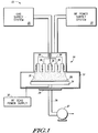
- FIG. 1 Shown in FIG. 1 is an ICP reactor 10.
- Inductively coupled plasma reactor 10 includes a processing chamber 12 housing a chuck 14.
- a plasma source 16 resides in an upper portion of processing chamber 12 in opposed spatial relationship to chuck 14.
- Processing chamber 12 is supplied with RF power from an RF power supply system 18.
- RF power supply system 18 contains a plurality of independent RF power supply generators each capable of operating at an independent power level and frequency.
- Processing chamber 12 is also supplied with processing gases from a gas supply system 20.
- gas supply system 20 is capable of supplying processing gas to processing chamber 12 in multiple independent gas feed lines. Vacuum pressure within processing chamber 12 is controlled by vacuum system 22.
- Reaction products and processing gases are withdrawn from processing chamber 12 through vacuum panel 24, which in a preferred arrangement, resides in processing chamber 12 below chuck 14 and coupled to vacuum line 26.
- vacuum panel 24 which in a preferred arrangement, resides in processing chamber 12 below chuck 14 and coupled to vacuum line 26.
- temperature control of chuck 14 can be provided by a cooling system (not shown). Either liquid or gas coolant can be transported through cooling channels embedded in chuck 14.
- plasma source 16 contains numerous channels with each channel supplied by independent gas feed lines 34, 35, and 36.
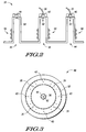
- FIG. 2 illustrates a portion of plasma source 16 in exploded cross-sectional view.
- Gas feed line 36 supplies central channel 38 through an inner gas plenum 40.
- a gas orifice 42 provides communication between central channel 38 and inner gas plenum 40.
- gas feed line 35 supplies processing gases to first channel 44 through an outer gas plenum 46.
- Plenum cap 50 houses inner gas plenum 40 distributing gas to central channel 38.
- plenum cap 52 distributes gas to outer gas plenum 46.
- Gas feed line 36 is attached to plenum cap 50 in a central portion thereof.
- Gas feed line 35 can be attached to plenum cap 52 at numerous sites, as illustrated in FIG. 3.
- gas orifice 43 is provided at numerous locations around the circular geometry of first channel 44.
- a central RF coil 54 surrounds central channel 38. Additionally, a first RF coil 56 surrounds first channel 44. Both central RF coil 54 and first RF coil 56 are independently controlled by RF power supply system 18. Each RF coil can supply an independent power level and RF frequency to the processing gases within the enclosed channel. RF coils 54 and 56 are separated from the processing gases within each channel by a dielectric housing 58. Electrical current traversing the RF coils inductively couples with processing gas species to ignite a plasma within each channel. Those skilled in the art will recognize that by independently powering each RF coil and by independently supplying each channel with processing gases that the plasma density and composition can be independently adjusted in each channel within plasma source 16.
- FIGs. 4 and 5 additional embodiments of an ICP reactor designed in accordance with the invention are illustrated in FIGs. 4 and 5.
- the plasma conditions experienced by semiconductor wafer 28 can be further controlled by varying the separation distance between portions of plasma source 16 and the surface of semiconductor wafer 28.
- central channel 38 is in close proximity to semiconductor wafer 28, while first channel 44 is vertically separated from semiconductor wafer 28.
- central channel 38 is vertically separated from semiconductor wafer 28 a greater distance than first channel 44.
- first channel 44 By varying the vertical separation distance between components of plasma source 16 and the semiconductor wafer being etched, an additional degree of control is provided for varying the plasma conditions across the surface of the semiconductor wafer.
- variable plasma conditions can be combined with varying degrees of RF bias applied to chuck 14 to enable even more precise control of ion bombardment upon semiconductor wafer 28.
- RF shields are positioned outside of each coil in plasma source 16. As illustrated in FIG. 5, a central RF shield 60 surrounds central RF coil 54, and a first RF shield 62 surrounds first RF coil 56. RF shields 60 and 62 minimize the RF interference between the independently powered coils in plasma source 16.
- the RF shields can be constructed from a conductive material such as aluminum, or alternatively a high-permeability, ferromagnetic material, such as a ferrite material.
- RF shields 60 and 62 can enhance the magnetic field within each channel by confining the magnetic field to the immediate region of the RF coils that they surround.
- shields 60 and 62 are depicted in the particular ICP reactor embodiment illustrated in FIG. 5, those skilled in the art will appreciate that shields 60 and 62 can be similarly incorporated into any of the plasma source configurations contemplated by the present invention.
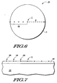
- FIG. 6 Shown in FIG. 6, in top view, is a generalized depiction of semiconductor wafer 28.
- Semiconductor wafer 28 has a generally circular geometry characterized by a radius "R" and by a perimeter "P.”
- Semiconductor wafer 28 can be further characterized by a plurality of locations 64 positioned on the surface of semiconductor wafer 28 and specified by a radial distance. The radial distance varies from zero to the radial distance of perimeter P.
- FIG. 7 illustrates, in cross-section, a portion of semiconductor wafer 28.
- a material layer 66 overlies the surface of semiconductor wafer 28.
- the process of the present invention contemplates, the removal of many different kinds of materials commonly used in the fabrication of integrated circuit devices.
- material layer 66 can be a semiconductor material, such as polycrystalline silicon, or a refractory metal silicide, or the like.
- material layer 66 can be a conductive material, such as aluminum, aluminum alloyed with silicon, aluminum alloyed with silicon and copper, elemental copper, and the like.
- material layer 66 can be a dielectric material, such as silicon dioxide, silicon nitride, silicon oxynitride, boron oxynitride, and the like.
- semiconductor wafer 28 is positioned on chuck 14 of ICP reactor 10 in such a manner that the center point, denoted "C" in FIGs. 6 and 7, is approximately vertically aligned with central channel 38 in plasma source 16.
- the localized etch rate at location 64 across semiconductor substrate 28 can be independently controlled by the spatially variant plasma conditions generated by plasma source 16. In this manner, radial control of the etch rate of material layer 66 is attained, such that material layer 66 in proximity to the perimeter P is etched simultaneously with portions of material layer 66 at center point C, and at the various location 64 across semiconductor wafer 28.
- semiconductor wafer 28 is positioned on chuck 14 of ICP reactor 10 in such a manner that the center point, denoted "C" in FIGs. 6 and 7, is approximately vertically aligned with central channel 38 in plasma source 16.
- the localized deposition rate at locations 64 across semiconductor substrate 28 can be independently controlled by the spatially variant plasma conditions generated by plasma source 16. In this manner, radial control of the deposition rate of material layer 66 is attained, such that portions of material layer 66 in proximity to the perimeter P are formed simultaneously with portions of material layer 66 at center point C, and at the various location 64 across semiconductor wafer 28.
- Semiconductor substrate 28 is first subjected to a chemical vapor deposition process to deposit a material layer 66 thereon. Semiconductor substrate 28 is then placed on chuck 14 in ICP reactor 10. Processing gas is selected depending upon the composition of the material layer to be etched. For example, where material layer 66 is polycrystalline silicon, halogen gases, such as chlorine, and hydrogenated halogen gases, such as hydrogen chloride and hydrogen bromide, are introduced together with an inert gas diluent. The total gas flow from gas supply system 20 is adjusted to a value of between 40 and 200 sccm and vacuum system 22 is adjusted to achieve a processing pressure of about 1 to 10 millitorr in processing chamber 12.
- halogen gases such as chlorine
- hydrogenated halogen gases such as hydrogen chloride and hydrogen bromide
- Semiconductor substrate 28 is placed on chuck 14 in ICP reactor 10.
- Processing gas is selected depending upon the composition of the material layer to deposited. For example, where material layer 66 is epitaxial silicon, hydrogen and silane are introduced in processing chamber 12 at about a 3:1 flow ratio.
- the total gas flow from gas supply system 20 is adjusted to a value of about 40 sccm and vacuum system 22 is adjusted to achieve a processing pressure of about 1 to 25 millitorr in processing chamber 12.
- RF power is then applied from RF power supply system 18 to RF coils 54 and 56 in plasma source 16.
- about 500 to 1500 watts RF is applied to RF coils 54 and 56 at a frequency of about 13.56MHz.
- about 0 to -60 volts DC is applied to chuck 14 while maintaining chuck 14 at a temperature of about 400 to 700°C.
- the plasma deposition of the material layer is then carried out to completion.
- the invention contemplates the use of many different kinds of chemical agents for the deposition or etching of a wide variety of materials used to form thin-film layers in semiconductor devices. It is therefore intended to include within the invention all such variations and modifications as fall within the scope of the appended claims and equivalents thereof.
Landscapes
- Chemical & Material Sciences (AREA)
- Engineering & Computer Science (AREA)
- Physics & Mathematics (AREA)
- Plasma & Fusion (AREA)
- Analytical Chemistry (AREA)
- Chemical Kinetics & Catalysis (AREA)
- General Chemical & Material Sciences (AREA)
- Materials Engineering (AREA)
- Mechanical Engineering (AREA)
- Metallurgy (AREA)
- Organic Chemistry (AREA)
- Plasma Technology (AREA)
- Drying Of Semiconductors (AREA)
- Chemical Vapour Deposition (AREA)
- ing And Chemical Polishing (AREA)
Applications Claiming Priority (2)
| Application Number | Priority Date | Filing Date | Title |
|---|---|---|---|
| US08/605,697 US5683548A (en) | 1996-02-22 | 1996-02-22 | Inductively coupled plasma reactor and process |
| US605697 | 1996-02-22 |
Publications (3)
| Publication Number | Publication Date |
|---|---|
| EP0792947A2 true EP0792947A2 (de) | 1997-09-03 |
| EP0792947A3 EP0792947A3 (de) | 1999-04-14 |
| EP0792947B1 EP0792947B1 (de) | 2005-11-16 |
Family
ID=24424805
Family Applications (1)
| Application Number | Title | Priority Date | Filing Date |
|---|---|---|---|
| EP97102279A Expired - Lifetime EP0792947B1 (de) | 1996-02-22 | 1997-02-13 | Verfahren mit einem induktiv gekoppelten Plasmareaktor |
Country Status (8)
| Country | Link |
|---|---|
| US (1) | US5683548A (de) |
| EP (1) | EP0792947B1 (de) |
| JP (1) | JP3959145B2 (de) |
| KR (1) | KR100386388B1 (de) |
| DE (1) | DE69734619T2 (de) |
| MX (1) | MX9700586A (de) |
| SG (1) | SG63686A1 (de) |
| TW (1) | TW373226B (de) |
Cited By (9)
| Publication number | Priority date | Publication date | Assignee | Title |
|---|---|---|---|---|
| WO1999048130A1 (en) * | 1998-03-14 | 1999-09-23 | Applied Materials, Inc. | Distributed inductively-coupled plasma source |
| DE19960092A1 (de) * | 1999-12-14 | 2001-07-12 | Bosch Gmbh Robert | Beschichtungsverfahren |
| WO2002003415A3 (en) * | 2000-06-30 | 2002-05-23 | Lam Res Corp | Switched uniformity control |
| WO2002059934A3 (en) * | 2001-01-23 | 2002-11-21 | Wafermasters Inc | Plasma generation apparatus and method |
| KR100469890B1 (ko) * | 2002-10-24 | 2005-02-02 | 주식회사 아이피에스 | 건식식각용 반도체 제조장치 |
| KR100532365B1 (ko) * | 2003-04-10 | 2005-11-30 | 주식회사 아이피에스 | 균일한 플라즈마를 제공하는 유도 결합형 다중 코일플라즈마 소스 |
| EP1168415A3 (de) * | 2000-06-23 | 2007-02-21 | Mitsubishi Heavy Industries, Ltd. | Antenne und Verfahren zu ihrer Spannungsversorgung |
| US11195705B2 (en) | 2017-03-29 | 2021-12-07 | Semes Co., Ltd. | Plasma generating unit and substrate treating apparatus comprising the same |
| TWI801915B (zh) * | 2020-09-16 | 2023-05-11 | 日商鎧俠股份有限公司 | 半導體製造裝置 |
Families Citing this family (113)
| Publication number | Priority date | Publication date | Assignee | Title |
|---|---|---|---|---|
| US6165311A (en) * | 1991-06-27 | 2000-12-26 | Applied Materials, Inc. | Inductively coupled RF plasma reactor having an overhead solenoidal antenna |
| US5653811A (en) * | 1995-07-19 | 1997-08-05 | Chan; Chung | System for the plasma treatment of large area substrates |
| JP4654176B2 (ja) * | 1996-02-22 | 2011-03-16 | 住友精密工業株式会社 | 誘導結合プラズマ・リアクタ |
| JPH1027762A (ja) * | 1996-03-18 | 1998-01-27 | Hyundai Electron Ind Co Ltd | 誘導結合形プラズマcvd方法及びこれを用いて生成された非晶質シリコン薄膜,及び、窒化シリコン膜,非晶質薄膜トランジスタ |
| JPH09251935A (ja) * | 1996-03-18 | 1997-09-22 | Applied Materials Inc | プラズマ点火装置、プラズマを用いる半導体製造装置及び半導体装置のプラズマ点火方法 |
| DE69719108D1 (de) * | 1996-05-02 | 2003-03-27 | Tokyo Electron Ltd | Plasmabehandlungsgerät |
| US5846883A (en) * | 1996-07-10 | 1998-12-08 | Cvc, Inc. | Method for multi-zone high-density inductively-coupled plasma generation |
| JP3640478B2 (ja) * | 1996-09-20 | 2005-04-20 | アネルバ株式会社 | プラズマ処理装置 |
| EP1324371B1 (de) * | 1996-09-27 | 2006-06-07 | Surface Technology Systems Plc | Plasmabearbeitungsvorrichtung |
| DE19643865C2 (de) * | 1996-10-30 | 1999-04-08 | Schott Glas | Plasmaunterstütztes chemisches Abscheidungsverfahren (CVD) mit entfernter Anregung eines Anregungsgases (Remote-Plasma-CVD-Verfahren) zur Beschichtung oder zur Behandlung großflächiger Substrate und Vorrichtung zur Durchführung desselben |
| US5981899A (en) * | 1997-01-17 | 1999-11-09 | Balzers Aktiengesellschaft | Capacitively coupled RF-plasma reactor |
| US6267074B1 (en) * | 1997-02-24 | 2001-07-31 | Foi Corporation | Plasma treatment systems |
| JP3483725B2 (ja) * | 1997-04-02 | 2004-01-06 | 株式会社日立製作所 | プラズマ処理装置及び処理方法 |
| US6158384A (en) * | 1997-06-05 | 2000-12-12 | Applied Materials, Inc. | Plasma reactor with multiple small internal inductive antennas |
| US5982100A (en) * | 1997-07-28 | 1999-11-09 | Pars, Inc. | Inductively coupled plasma reactor |
| JP3814813B2 (ja) * | 1997-09-01 | 2006-08-30 | 株式会社エフオーアイ | プラズマ発生装置 |
| US6028395A (en) * | 1997-09-16 | 2000-02-22 | Lam Research Corporation | Vacuum plasma processor having coil with added conducting segments to its peripheral part |
| JP4104193B2 (ja) * | 1997-11-14 | 2008-06-18 | 株式会社エフオーアイ | プラズマ処理装置 |
| US6028285A (en) * | 1997-11-19 | 2000-02-22 | Board Of Regents, The University Of Texas System | High density plasma source for semiconductor processing |
| US6136165A (en) * | 1997-11-26 | 2000-10-24 | Cvc Products, Inc. | Apparatus for inductively-coupled-plasma-enhanced ionized physical-vapor deposition |
| US6274459B1 (en) | 1998-02-17 | 2001-08-14 | Silicon Genesis Corporation | Method for non mass selected ion implant profile control |
| JP3868620B2 (ja) * | 1998-03-02 | 2007-01-17 | 株式会社エフオーアイ | プラズマ発生装置 |
| JP4001355B2 (ja) * | 1998-03-02 | 2007-10-31 | 株式会社エフオーアイ | プラズマ発生装置 |
| US5980686A (en) * | 1998-04-15 | 1999-11-09 | Applied Komatsu Technology, Inc. | System and method for gas distribution in a dry etch process |
| JP3567736B2 (ja) * | 1998-05-25 | 2004-09-22 | 株式会社日立製作所 | プラズマ処理装置 |
| US6204607B1 (en) * | 1998-05-28 | 2001-03-20 | Applied Komatsu Technology, Inc. | Plasma source with multiple magnetic flux sources each having a ferromagnetic core |
| US6211092B1 (en) * | 1998-07-09 | 2001-04-03 | Applied Materials, Inc. | Counterbore dielectric plasma etch process particularly useful for dual damascene |
| US6218640B1 (en) * | 1999-07-19 | 2001-04-17 | Timedomain Cvd, Inc. | Atmospheric pressure inductive plasma apparatus |
| JP4046207B2 (ja) * | 1998-08-06 | 2008-02-13 | 株式会社エフオーアイ | プラズマ処理装置 |
| US6235640B1 (en) * | 1998-09-01 | 2001-05-22 | Lam Research Corporation | Techniques for forming contact holes through to a silicon layer of a substrate |
| JP4056144B2 (ja) * | 1998-09-10 | 2008-03-05 | 株式会社エフオーアイ | プラズマ処理装置 |
| US6218251B1 (en) | 1998-11-06 | 2001-04-17 | Advanced Micro Devices, Inc. | Asymmetrical IGFET devices with spacers formed by HDP techniques |
| KR100311234B1 (ko) * | 1999-01-18 | 2001-11-02 | 학교법인 인하학원 | 고품위 유도결합 플라즈마 리액터 |
| US6348389B1 (en) * | 1999-03-11 | 2002-02-19 | Taiwan Semiconductor Manufacturing Company | Method of forming and etching a resist protect oxide layer including end-point etch |
| US6165567A (en) * | 1999-04-12 | 2000-12-26 | Motorola, Inc. | Process of forming a semiconductor device |
| US6458723B1 (en) | 1999-06-24 | 2002-10-01 | Silicon Genesis Corporation | High temperature implant apparatus |
| JP3385528B2 (ja) | 1999-07-06 | 2003-03-10 | 日本電気株式会社 | ドライエッチング装置とドライエッチング方法 |
| US6368988B1 (en) * | 1999-07-16 | 2002-04-09 | Micron Technology, Inc. | Combined gate cap or digit line and spacer deposition using HDP |
| US6287643B1 (en) * | 1999-09-30 | 2001-09-11 | Novellus Systems, Inc. | Apparatus and method for injecting and modifying gas concentration of a meta-stable or atomic species in a downstream plasma reactor |
| WO2001037314A1 (en) * | 1999-11-15 | 2001-05-25 | Lam Research Corporation | Materials and gas chemistries for processing systems |
| DE10060002B4 (de) * | 1999-12-07 | 2016-01-28 | Komatsu Ltd. | Vorrichtung zur Oberflächenbehandlung |
| US6367412B1 (en) * | 2000-02-17 | 2002-04-09 | Applied Materials, Inc. | Porous ceramic liner for a plasma source |
| AU2001239906A1 (en) * | 2000-03-01 | 2001-09-12 | Tokyo Electron Limited | Electrically controlled plasma uniformity in a high density plasma source |
| JP2001267305A (ja) * | 2000-03-17 | 2001-09-28 | Hitachi Ltd | プラズマ処理装置 |
| US6459066B1 (en) | 2000-08-25 | 2002-10-01 | Board Of Regents, The University Of Texas System | Transmission line based inductively coupled plasma source with stable impedance |
| US6875700B2 (en) * | 2000-08-29 | 2005-04-05 | Board Of Regents, The University Of Texas System | Ion-Ion plasma processing with bias modulation synchronized to time-modulated discharges |
| JP2002100623A (ja) * | 2000-09-20 | 2002-04-05 | Fuji Daiichi Seisakusho:Kk | 薄膜半導体製造装置 |
| JP4120561B2 (ja) * | 2000-10-03 | 2008-07-16 | 松下電器産業株式会社 | プラズマ処理方法およびプラズマ処理装置 |
| US6471830B1 (en) | 2000-10-03 | 2002-10-29 | Veeco/Cvc, Inc. | Inductively-coupled-plasma ionized physical-vapor deposition apparatus, method and system |
| US6534423B1 (en) * | 2000-12-27 | 2003-03-18 | Novellus Systems, Inc. | Use of inductively-coupled plasma in plasma-enhanced chemical vapor deposition reactor to improve film-to-wall adhesion following in-situ plasma clean |
| US7510664B2 (en) * | 2001-01-30 | 2009-03-31 | Rapt Industries, Inc. | Apparatus and method for atmospheric pressure reactive atom plasma processing for shaping of damage free surfaces |
| US7591957B2 (en) * | 2001-01-30 | 2009-09-22 | Rapt Industries, Inc. | Method for atmospheric pressure reactive atom plasma processing for surface modification |
| JP4471514B2 (ja) * | 2001-02-26 | 2010-06-02 | 株式会社エフオーアイ | プラズマ処理装置 |
| US6652711B2 (en) | 2001-06-06 | 2003-11-25 | Tokyo Electron Limited | Inductively-coupled plasma processing system |
| US6893971B2 (en) * | 2001-07-19 | 2005-05-17 | Matsushita Electric Industrial Co., Ltd. | Dry etching method and apparatus |
| KR200253559Y1 (ko) * | 2001-07-30 | 2001-11-22 | 주식회사 플라즈마트 | 회전방향으로 균일한 플라즈마 밀도를 발생시키는유도결합형 플라즈마 발생장치의 안테나구조 |
| US6676760B2 (en) | 2001-08-16 | 2004-01-13 | Appiled Materials, Inc. | Process chamber having multiple gas distributors and method |
| US6660177B2 (en) * | 2001-11-07 | 2003-12-09 | Rapt Industries Inc. | Apparatus and method for reactive atom plasma processing for material deposition |
| US6887341B2 (en) * | 2001-11-13 | 2005-05-03 | Tokyo Electron Limited | Plasma processing apparatus for spatial control of dissociation and ionization |
| US6913652B2 (en) * | 2002-06-17 | 2005-07-05 | Applied Materials, Inc. | Gas flow division in a wafer processing system having multiple chambers |
| KR100481311B1 (ko) * | 2002-09-19 | 2005-04-07 | 최대규 | 플라즈마 프로세스 챔버 |
| KR100500852B1 (ko) * | 2002-10-10 | 2005-07-12 | 최대규 | 원격 플라즈마 발생기 |
| DE10247913A1 (de) * | 2002-10-14 | 2004-04-22 | Robert Bosch Gmbh | Plasmaanlage und Verfahren zum anisotropen Einätzen von Strukturen in ein Substrat |
| KR100488348B1 (ko) * | 2002-11-14 | 2005-05-10 | 최대규 | 플라즈마 프로세스 챔버 및 시스템 |
| JP4753276B2 (ja) * | 2002-11-26 | 2011-08-24 | 東京エレクトロン株式会社 | プラズマ処理方法及びプラズマ処理装置 |
| US7371992B2 (en) * | 2003-03-07 | 2008-05-13 | Rapt Industries, Inc. | Method for non-contact cleaning of a surface |
| US7304263B2 (en) * | 2003-08-14 | 2007-12-04 | Rapt Industries, Inc. | Systems and methods utilizing an aperture with a reactive atom plasma torch |
| US7297892B2 (en) * | 2003-08-14 | 2007-11-20 | Rapt Industries, Inc. | Systems and methods for laser-assisted plasma processing |
| US6829056B1 (en) | 2003-08-21 | 2004-12-07 | Michael Barnes | Monitoring dimensions of features at different locations in the processing of substrates |
| US20050255245A1 (en) * | 2004-01-13 | 2005-11-17 | Fanton Mark A | Method and apparatus for the chemical vapor deposition of materials |
| KR100661350B1 (ko) * | 2004-12-27 | 2006-12-27 | 삼성전자주식회사 | Mems 소자 패키지 및 그 제조방법 |
| JP4961111B2 (ja) * | 2005-02-28 | 2012-06-27 | 富士フイルム株式会社 | 光電変換膜積層型固体撮像素子とその製造方法 |
| KR100709354B1 (ko) * | 2005-06-17 | 2007-04-20 | 삼성전자주식회사 | 다채널 플라즈마 가속장치 |
| KR100689848B1 (ko) * | 2005-07-22 | 2007-03-08 | 삼성전자주식회사 | 기판처리장치 |
| JP4593413B2 (ja) | 2005-09-15 | 2010-12-08 | 株式会社日立ハイテクノロジーズ | プラズマ処理方法及び処理装置 |
| JP4405973B2 (ja) * | 2006-01-17 | 2010-01-27 | キヤノンアネルバ株式会社 | 薄膜作製装置 |
| KR101501426B1 (ko) * | 2006-06-02 | 2015-03-11 | 어플라이드 머티어리얼스, 인코포레이티드 | 차압 측정들에 의한 가스 유동 제어 |
| US7879184B2 (en) * | 2006-06-20 | 2011-02-01 | Lam Research Corporation | Apparatuses, systems and methods for rapid cleaning of plasma confinement rings with minimal erosion of other chamber parts |
| JP4094040B2 (ja) * | 2006-08-18 | 2008-06-04 | 株式会社エフオーアイ | プラズマ発生装置 |
| US7829815B2 (en) * | 2006-09-22 | 2010-11-09 | Taiwan Semiconductor Manufacturing Co., Ltd. | Adjustable electrodes and coils for plasma density distribution control |
| JP2008091750A (ja) * | 2006-10-04 | 2008-04-17 | Hitachi Kokusai Electric Inc | アッシング装置 |
| EP2109878A4 (de) * | 2007-02-15 | 2012-03-14 | Applied Materials Inc | System und verfahren zur steuerung eines chemischen aufdampfungsprozesses |
| EP2121816A1 (de) * | 2007-02-15 | 2009-11-25 | Applied Materials, Inc. | Lokalisiertes mikrowellenquellenarraypumpen zur steuerung des lokalisierten partialdrucks bei flachen und dreidimensionalen pecvd-beschichtungen |
| JP4932857B2 (ja) * | 2007-02-16 | 2012-05-16 | ラム リサーチ コーポレーション | 誘導コイル、プラズマ発生装置およびプラズマ発生方法 |
| US20080236491A1 (en) * | 2007-03-30 | 2008-10-02 | Tokyo Electron Limited | Multiflow integrated icp source |
| US7976674B2 (en) * | 2007-06-13 | 2011-07-12 | Tokyo Electron Limited | Embedded multi-inductive large area plasma source |
| US8528498B2 (en) * | 2007-06-29 | 2013-09-10 | Lam Research Corporation | Integrated steerability array arrangement for minimizing non-uniformity |
| US9105449B2 (en) * | 2007-06-29 | 2015-08-11 | Lam Research Corporation | Distributed power arrangements for localizing power delivery |
| GB0713821D0 (en) | 2007-07-17 | 2007-08-29 | P2I Ltd | A plasma deposition apparatus |
| US8021487B2 (en) * | 2007-12-12 | 2011-09-20 | Veeco Instruments Inc. | Wafer carrier with hub |
| JP5297048B2 (ja) * | 2008-01-28 | 2013-09-25 | 三菱重工業株式会社 | プラズマ処理方法及びプラズマ処理装置 |
| JP5262206B2 (ja) | 2008-03-12 | 2013-08-14 | 豊田合成株式会社 | Iii族窒化物半導体層の製造方法及びiii族窒化物半導体発光素子の製造方法 |
| US7994724B2 (en) * | 2009-03-27 | 2011-08-09 | Ecole Polytechnique | Inductive plasma applicator |
| FI124414B (fi) * | 2010-04-30 | 2014-08-29 | Beneq Oy | Lähde ja järjestely substraatin käsittelemiseksi |
| US20110278260A1 (en) * | 2010-05-14 | 2011-11-17 | Applied Materials, Inc. | Inductive plasma source with metallic shower head using b-field concentrator |
| JP5735232B2 (ja) * | 2010-08-02 | 2015-06-17 | 株式会社イー・エム・ディー | プラズマ処理装置 |
| US9793126B2 (en) * | 2010-08-04 | 2017-10-17 | Lam Research Corporation | Ion to neutral control for wafer processing with dual plasma source reactor |
| US20130059092A1 (en) * | 2011-09-07 | 2013-03-07 | Applied Materials, Inc. | Method and apparatus for gas distribution and plasma application in a linear deposition chamber |
| US10271416B2 (en) * | 2011-10-28 | 2019-04-23 | Applied Materials, Inc. | High efficiency triple-coil inductively coupled plasma source with phase control |
| DE102012017453A1 (de) | 2012-09-04 | 2014-03-06 | Manz Ag | Plasmabehandlungseinrichtung und Verfahren zur Behandlung zumindest eines Substrats |
| CN103906338B (zh) * | 2012-12-31 | 2016-06-08 | 北京北方微电子基地设备工艺研究中心有限责任公司 | 一种等离子体装置 |
| US9245761B2 (en) | 2013-04-05 | 2016-01-26 | Lam Research Corporation | Internal plasma grid for semiconductor fabrication |
| GB201309583D0 (en) * | 2013-05-29 | 2013-07-10 | Spts Technologies Ltd | Apparatus for processing a semiconductor workpiece |
| KR101526507B1 (ko) * | 2013-11-15 | 2015-06-09 | 피에스케이 주식회사 | 기판 처리 장치 및 방법 |
| US20170092470A1 (en) * | 2015-09-28 | 2017-03-30 | Applied Materials, Inc. | Plasma reactor for processing a workpiece with an array of plasma point sources |
| JP6857799B2 (ja) * | 2016-03-29 | 2021-04-14 | パナソニックIpマネジメント株式会社 | プラズマ処理装置及びプラズマ処理方法、電子デバイスの製造方法 |
| KR101932859B1 (ko) * | 2017-10-16 | 2019-03-20 | 성균관대학교산학협력단 | 플라즈마 소스 및 이를 이용한 플라즈마 발생장치 |
| US11177067B2 (en) * | 2018-07-25 | 2021-11-16 | Lam Research Corporation | Magnetic shielding for plasma sources |
| JP7169885B2 (ja) * | 2019-01-10 | 2022-11-11 | 東京エレクトロン株式会社 | 誘導結合プラズマ処理装置 |
| KR102189337B1 (ko) * | 2019-07-17 | 2020-12-09 | 주식회사 유진테크 | 플라즈마 처리 장치 |
| US11150120B2 (en) * | 2019-09-22 | 2021-10-19 | Applied Materials, Inc. | Low temperature thermal flow ratio controller |
| US20210098230A1 (en) * | 2019-09-27 | 2021-04-01 | Applied Materials, Inc. | Monolithic modular high-frequency plasma source |
| TWI714366B (zh) * | 2019-11-26 | 2020-12-21 | 聚昌科技股份有限公司 | 線圈垂直位置可動態調整之蝕刻機結構 |
Family Cites Families (8)
| Publication number | Priority date | Publication date | Assignee | Title |
|---|---|---|---|---|
| JPS59129772A (ja) * | 1983-01-18 | 1984-07-26 | Ushio Inc | 光化学蒸着装置 |
| DE3830249A1 (de) * | 1988-09-06 | 1990-03-15 | Schott Glaswerke | Plasmaverfahren zum beschichten ebener substrate |
| US5091049A (en) * | 1989-06-13 | 1992-02-25 | Plasma & Materials Technologies, Inc. | High density plasma deposition and etching apparatus |
| US5134965A (en) * | 1989-06-16 | 1992-08-04 | Hitachi, Ltd. | Processing apparatus and method for plasma processing |
| US5269847A (en) * | 1990-08-23 | 1993-12-14 | Applied Materials, Inc. | Variable rate distribution gas flow reaction chamber |
| US5356515A (en) * | 1990-10-19 | 1994-10-18 | Tokyo Electron Limited | Dry etching method |
| US5241245A (en) * | 1992-05-06 | 1993-08-31 | International Business Machines Corporation | Optimized helical resonator for plasma processing |
| US5449432A (en) * | 1993-10-25 | 1995-09-12 | Applied Materials, Inc. | Method of treating a workpiece with a plasma and processing reactor having plasma igniter and inductive coupler for semiconductor fabrication |
-
1996
- 1996-02-22 US US08/605,697 patent/US5683548A/en not_active Expired - Lifetime
- 1996-12-19 TW TW085115688A patent/TW373226B/zh not_active IP Right Cessation
-
1997
- 1997-01-08 SG SG1997000029A patent/SG63686A1/en unknown
- 1997-01-22 MX MX9700586A patent/MX9700586A/es unknown
- 1997-02-13 EP EP97102279A patent/EP0792947B1/de not_active Expired - Lifetime
- 1997-02-13 DE DE69734619T patent/DE69734619T2/de not_active Expired - Lifetime
- 1997-02-18 JP JP04988897A patent/JP3959145B2/ja not_active Expired - Lifetime
- 1997-02-22 KR KR1019970005425A patent/KR100386388B1/ko not_active Expired - Lifetime
Non-Patent Citations (1)
| Title |
|---|
| None |
Cited By (15)
| Publication number | Priority date | Publication date | Assignee | Title |
|---|---|---|---|---|
| WO1999048130A1 (en) * | 1998-03-14 | 1999-09-23 | Applied Materials, Inc. | Distributed inductively-coupled plasma source |
| DE19960092A1 (de) * | 1999-12-14 | 2001-07-12 | Bosch Gmbh Robert | Beschichtungsverfahren |
| EP1912246A3 (de) * | 2000-06-23 | 2010-04-28 | Mitsubishi Heavy Industries, Ltd. | Energieversorgungsantenne und Energieversorgungsverfahren |
| US7520246B2 (en) | 2000-06-23 | 2009-04-21 | Mitsubishi Heavy Industries, Ltd. | Power supply antenna and power supply method |
| EP1168415A3 (de) * | 2000-06-23 | 2007-02-21 | Mitsubishi Heavy Industries, Ltd. | Antenne und Verfahren zu ihrer Spannungsversorgung |
| US7282454B2 (en) | 2000-06-30 | 2007-10-16 | Lam Research Corporation | Switched uniformity control |
| WO2002003415A3 (en) * | 2000-06-30 | 2002-05-23 | Lam Res Corp | Switched uniformity control |
| US6632322B1 (en) | 2000-06-30 | 2003-10-14 | Lam Research Corporation | Switched uniformity control |
| KR100865054B1 (ko) * | 2000-06-30 | 2008-10-23 | 램 리써치 코포레이션 | 스위칭 방식 균일성 제어 |
| WO2002059934A3 (en) * | 2001-01-23 | 2002-11-21 | Wafermasters Inc | Plasma generation apparatus and method |
| US6633132B2 (en) | 2001-01-23 | 2003-10-14 | Wafermasters Inc. | Plasma gereration apparatus and method |
| KR100469890B1 (ko) * | 2002-10-24 | 2005-02-02 | 주식회사 아이피에스 | 건식식각용 반도체 제조장치 |
| KR100532365B1 (ko) * | 2003-04-10 | 2005-11-30 | 주식회사 아이피에스 | 균일한 플라즈마를 제공하는 유도 결합형 다중 코일플라즈마 소스 |
| US11195705B2 (en) | 2017-03-29 | 2021-12-07 | Semes Co., Ltd. | Plasma generating unit and substrate treating apparatus comprising the same |
| TWI801915B (zh) * | 2020-09-16 | 2023-05-11 | 日商鎧俠股份有限公司 | 半導體製造裝置 |
Also Published As
| Publication number | Publication date |
|---|---|
| MX9700586A (es) | 1997-08-30 |
| DE69734619D1 (de) | 2005-12-22 |
| EP0792947A3 (de) | 1999-04-14 |
| EP0792947B1 (de) | 2005-11-16 |
| DE69734619T2 (de) | 2006-06-08 |
| KR970063563A (ko) | 1997-09-12 |
| TW373226B (en) | 1999-11-01 |
| JP3959145B2 (ja) | 2007-08-15 |
| US5683548A (en) | 1997-11-04 |
| KR100386388B1 (ko) | 2003-08-14 |
| SG63686A1 (en) | 1999-03-30 |
| JPH09237698A (ja) | 1997-09-09 |
Similar Documents
| Publication | Publication Date | Title |
|---|---|---|
| US5683548A (en) | Inductively coupled plasma reactor and process | |
| MXPA97000586A (es) | Reactor de plasma acoplado inductivamente yproceso para fabricar un dispositivo semiconductor | |
| EP1444717B1 (de) | Abstimmbares mehrzonen-gasinjektionssystem | |
| US5824605A (en) | Gas dispersion window for plasma apparatus and method of use thereof | |
| US6415736B1 (en) | Gas distribution apparatus for semiconductor processing | |
| US6499425B1 (en) | Quasi-remote plasma processing method and apparatus | |
| KR101494469B1 (ko) | 반도체 기판을 균일하게 에칭하기 위한 가스 주입 | |
| EP0839217B1 (de) | Plasmaunterstützter chemischer reaktor und verfahren | |
| US7955986B2 (en) | Capacitively coupled plasma reactor with magnetic plasma control | |
| US6887341B2 (en) | Plasma processing apparatus for spatial control of dissociation and ionization | |
| US20090056629A1 (en) | Cathode liner with wafer edge gas injection in a plasma reactor chamber | |
| CN115398602B (zh) | 等离子处理装置以及等离子处理方法 | |
| US6435197B2 (en) | Method of cleaning a semiconductor fabricating apparatus | |
| US20040163595A1 (en) | Plasma processing apparatus | |
| JP5250611B2 (ja) | 誘導結合プラズマ・リアクタ | |
| US6027662A (en) | Materials processing by separately generated process medium constituents | |
| JPH11340146A (ja) | プラズマ処理装置 |
Legal Events
| Date | Code | Title | Description |
|---|---|---|---|
| PUAI | Public reference made under article 153(3) epc to a published international application that has entered the european phase |
Free format text: ORIGINAL CODE: 0009012 |
|
| AK | Designated contracting states |
Kind code of ref document: A2 Designated state(s): DE FR GB IE IT |
|
| RIN1 | Information on inventor provided before grant (corrected) |
Inventor name: ARNOLD, JOHN C. Inventor name: HARTIG, MICHAEL J. |
|
| PUAL | Search report despatched |
Free format text: ORIGINAL CODE: 0009013 |
|
| AK | Designated contracting states |
Kind code of ref document: A3 Designated state(s): DE FR GB IE IT |
|
| 17P | Request for examination filed |
Effective date: 19991014 |
|
| 17Q | First examination report despatched |
Effective date: 19991217 |
|
| RAP1 | Party data changed (applicant data changed or rights of an application transferred) |
Owner name: FREESCALE SEMICONDUCTOR, INC. |
|
| GRAP | Despatch of communication of intention to grant a patent |
Free format text: ORIGINAL CODE: EPIDOSNIGR1 |
|
| GRAS | Grant fee paid |
Free format text: ORIGINAL CODE: EPIDOSNIGR3 |
|
| GRAA | (expected) grant |
Free format text: ORIGINAL CODE: 0009210 |
|
| AK | Designated contracting states |
Kind code of ref document: B1 Designated state(s): DE FR GB IE IT |
|
| REG | Reference to a national code |
Ref country code: GB Ref legal event code: FG4D |
|
| REG | Reference to a national code |
Ref country code: IE Ref legal event code: FG4D |
|
| REF | Corresponds to: |
Ref document number: 69734619 Country of ref document: DE Date of ref document: 20051222 Kind code of ref document: P |
|
| ET | Fr: translation filed | ||
| PLBE | No opposition filed within time limit |
Free format text: ORIGINAL CODE: 0009261 |
|
| STAA | Information on the status of an ep patent application or granted ep patent |
Free format text: STATUS: NO OPPOSITION FILED WITHIN TIME LIMIT |
|
| 26N | No opposition filed |
Effective date: 20060817 |
|
| REG | Reference to a national code |
Ref country code: GB Ref legal event code: 732E Free format text: REGISTERED BETWEEN 20100729 AND 20100804 |
|
| REG | Reference to a national code |
Ref country code: FR Ref legal event code: TP |
|
| REG | Reference to a national code |
Ref country code: DE Ref legal event code: R082 Ref document number: 69734619 Country of ref document: DE Representative=s name: KRAMER - BARSKE - SCHMIDTCHEN, DE Effective date: 20120308 Ref country code: DE Ref legal event code: R082 Ref document number: 69734619 Country of ref document: DE Representative=s name: KRAMER BARSKE SCHMIDTCHEN PATENTANWAELTE PARTG, DE Effective date: 20120308 Ref country code: DE Ref legal event code: R081 Ref document number: 69734619 Country of ref document: DE Owner name: SPP PROCESS TECHNOLOGY SYSTEMS UK LTD., NEWPOR, GB Free format text: FORMER OWNER: SUMITOMO PRECISION PRODUCTS CO. LTD., AMAGASAKI, HYOGO, JP Effective date: 20120308 |
|
| REG | Reference to a national code |
Ref country code: FR Ref legal event code: PLFP Year of fee payment: 20 |
|
| PGFP | Annual fee paid to national office [announced via postgrant information from national office to epo] |
Ref country code: IE Payment date: 20160222 Year of fee payment: 20 Ref country code: DE Payment date: 20160223 Year of fee payment: 20 Ref country code: IT Payment date: 20160222 Year of fee payment: 20 |
|
| PGFP | Annual fee paid to national office [announced via postgrant information from national office to epo] |
Ref country code: FR Payment date: 20160222 Year of fee payment: 20 Ref country code: GB Payment date: 20160222 Year of fee payment: 20 |
|
| REG | Reference to a national code |
Ref country code: DE Ref legal event code: R071 Ref document number: 69734619 Country of ref document: DE |
|
| REG | Reference to a national code |
Ref country code: GB Ref legal event code: PE20 Expiry date: 20170212 |
|
| REG | Reference to a national code |
Ref country code: IE Ref legal event code: MK9A |
|
| PG25 | Lapsed in a contracting state [announced via postgrant information from national office to epo] |
Ref country code: GB Free format text: LAPSE BECAUSE OF EXPIRATION OF PROTECTION Effective date: 20170212 Ref country code: IE Free format text: LAPSE BECAUSE OF EXPIRATION OF PROTECTION Effective date: 20170213 |