EP0793016A2 - Electrode pour supprimer les ondes électriques de bruit parasite et procédé de fabrication de celle-ci - Google Patents
Electrode pour supprimer les ondes électriques de bruit parasite et procédé de fabrication de celle-ci Download PDFInfo
- Publication number
- EP0793016A2 EP0793016A2 EP97106728A EP97106728A EP0793016A2 EP 0793016 A2 EP0793016 A2 EP 0793016A2 EP 97106728 A EP97106728 A EP 97106728A EP 97106728 A EP97106728 A EP 97106728A EP 0793016 A2 EP0793016 A2 EP 0793016A2
- Authority
- EP
- European Patent Office
- Prior art keywords
- layer
- electrode
- electric wave
- substrate
- noise electric
- Prior art date
- Legal status (The legal status is an assumption and is not a legal conclusion. Google has not performed a legal analysis and makes no representation as to the accuracy of the status listed.)
- Granted
Links
Images






Classifications
-
- F—MECHANICAL ENGINEERING; LIGHTING; HEATING; WEAPONS; BLASTING
- F02—COMBUSTION ENGINES; HOT-GAS OR COMBUSTION-PRODUCT ENGINE PLANTS
- F02P—IGNITION, OTHER THAN COMPRESSION IGNITION, FOR INTERNAL-COMBUSTION ENGINES; TESTING OF IGNITION TIMING IN COMPRESSION-IGNITION ENGINES
- F02P7/00—Arrangements of distributors, circuit-makers or -breakers, e.g. of distributor and circuit-breaker combinations or pick-up devices
- F02P7/02—Arrangements of distributors, circuit-makers or -breakers, e.g. of distributor and circuit-breaker combinations or pick-up devices of distributors
-
- H—ELECTRICITY
- H01—ELECTRIC ELEMENTS
- H01R—ELECTRICALLY-CONDUCTIVE CONNECTIONS; STRUCTURAL ASSOCIATIONS OF A PLURALITY OF MUTUALLY-INSULATED ELECTRICAL CONNECTING ELEMENTS; COUPLING DEVICES; CURRENT COLLECTORS
- H01R39/00—Rotary current collectors, distributors or interrupters
- H01R39/60—Devices for interrupted current collection, e.g. commutating device, distributor, interrupter
-
- F—MECHANICAL ENGINEERING; LIGHTING; HEATING; WEAPONS; BLASTING
- F02—COMBUSTION ENGINES; HOT-GAS OR COMBUSTION-PRODUCT ENGINE PLANTS
- F02P—IGNITION, OTHER THAN COMPRESSION IGNITION, FOR INTERNAL-COMBUSTION ENGINES; TESTING OF IGNITION TIMING IN COMPRESSION-IGNITION ENGINES
- F02P7/00—Arrangements of distributors, circuit-makers or -breakers, e.g. of distributor and circuit-breaker combinations or pick-up devices
- F02P7/02—Arrangements of distributors, circuit-makers or -breakers, e.g. of distributor and circuit-breaker combinations or pick-up devices of distributors
- F02P7/021—Mechanical distributors
- F02P7/025—Mechanical distributors with noise suppression means specially adapted for the distributor
-
- Y—GENERAL TAGGING OF NEW TECHNOLOGICAL DEVELOPMENTS; GENERAL TAGGING OF CROSS-SECTIONAL TECHNOLOGIES SPANNING OVER SEVERAL SECTIONS OF THE IPC; TECHNICAL SUBJECTS COVERED BY FORMER USPC CROSS-REFERENCE ART COLLECTIONS [XRACs] AND DIGESTS
- Y10—TECHNICAL SUBJECTS COVERED BY FORMER USPC
- Y10S—TECHNICAL SUBJECTS COVERED BY FORMER USPC CROSS-REFERENCE ART COLLECTIONS [XRACs] AND DIGESTS
- Y10S428/00—Stock material or miscellaneous articles
- Y10S428/901—Printed circuit
-
- Y—GENERAL TAGGING OF NEW TECHNOLOGICAL DEVELOPMENTS; GENERAL TAGGING OF CROSS-SECTIONAL TECHNOLOGIES SPANNING OVER SEVERAL SECTIONS OF THE IPC; TECHNICAL SUBJECTS COVERED BY FORMER USPC CROSS-REFERENCE ART COLLECTIONS [XRACs] AND DIGESTS
- Y10—TECHNICAL SUBJECTS COVERED BY FORMER USPC
- Y10T—TECHNICAL SUBJECTS COVERED BY FORMER US CLASSIFICATION
- Y10T428/00—Stock material or miscellaneous articles
- Y10T428/24—Structurally defined web or sheet [e.g., overall dimension, etc.]
- Y10T428/24802—Discontinuous or differential coating, impregnation or bond [e.g., artwork, printing, retouched photograph, etc.]
- Y10T428/24917—Discontinuous or differential coating, impregnation or bond [e.g., artwork, printing, retouched photograph, etc.] including metal layer
-
- Y—GENERAL TAGGING OF NEW TECHNOLOGICAL DEVELOPMENTS; GENERAL TAGGING OF CROSS-SECTIONAL TECHNOLOGIES SPANNING OVER SEVERAL SECTIONS OF THE IPC; TECHNICAL SUBJECTS COVERED BY FORMER USPC CROSS-REFERENCE ART COLLECTIONS [XRACs] AND DIGESTS
- Y10—TECHNICAL SUBJECTS COVERED BY FORMER USPC
- Y10T—TECHNICAL SUBJECTS COVERED BY FORMER US CLASSIFICATION
- Y10T428/00—Stock material or miscellaneous articles
- Y10T428/24—Structurally defined web or sheet [e.g., overall dimension, etc.]
- Y10T428/24802—Discontinuous or differential coating, impregnation or bond [e.g., artwork, printing, retouched photograph, etc.]
- Y10T428/24926—Discontinuous or differential coating, impregnation or bond [e.g., artwork, printing, retouched photograph, etc.] including ceramic, glass, porcelain or quartz layer
Definitions
- This invention relates to an electrode for preventing noise electric wave and a method thereof which prevents the generation of noise electric wave, especially, the generation of noise electric wave for the radio which is loaded on automobiles and the like.
- the electrode according to the present invention is used as a rotor electrode of distributor of automobiles.
- a rotor electrode rotates to intermittently oppose a side-fixed electrode having a small clearance between them.
- the rotor electrode and the side-fixed electrode discharge between them so that they feed a number of ignition plugs.
- noise electric wave ignition noise
- the noise electric wave has wide and high frequency band, it causes hindrance on radiocommunication such as TV or radio, electronic equipments loaded on automobiles and the like; for example, EFI (electronical controlled fuel injection apparatus), ESC (electronic skid control apparatus), EAT (electronic control automatic transmission).
- the above spark discharge current comprises capacity discharge current and induction discharge current.
- the capacity discharge current is high-frequency current which flows for 10 micron seconds from the beginning of discharge at the initial discharge stage due to rapid build-up.
- the induction discharge current is low-frequency current (about 10 to 100mA) which continuously flows for 500 to 1500 micron seconds soon after the capacity discharge current flows.
- Ignition energy supplied for the ignition plug is proportionated with the product of the induction discharge current and its discharge duration.
- Concerning the induction discharge current since the absolute value level of the current value is low, it has little influence on the noise electric wave. Therefore, in order to effectively prevent the noise electric wave without decreasing the ignition energy, it is important that the starting voltage and the capacity discharge current are firmly decreased.
- Japanese Patent Registration No. 858984 discloses that high electrical resistance substance is formed on the surface of the discharge electrode in order to prevent the generation of noise electric wave caused by discharge gap. However, in this method, only 5 to 6dB of noise can be decreased so that required performance cannot be achieved.
- Japanese Unexamined Patent Publication No. 50735/1979 discloses the technique in which the discharge electrode which is one element of ignition distributor of internal combustion is performed by surface treatment so that the starting voltage and the capacity discharge current are decreased, thereby preventing noise electric wave.
- mixed powder comprising CuO (cupric oxide) and Al 2 O 3 (alumina) is thermal sprayed on the surface of the discharge electrode to form the layer for preventing noise electric wave.
- the layer for prevention of noise electric wave is formed on the surface of the discharge electrode which is faced to an opposite electrode.
- preliminary micro discharge is generated between CuO as oxide resistor and Al 2 O 3 as oxide dielectric substance, so main discharge voltage generated between CuO and the opposite electrode is reduced, thereby decreasing the capacity discharge current.
- the effect of the preliminary micro discharge is called as Malter effect, and the method for preventing noise electric wave which makes use of Malter effect is recently noticed.
- Japanese Examined Patent Publication No. 22472/1989 discloses one example of the electrode for preventing noise electric wave which makes use of Malter effect.
- This electrode comprises an electrode substrate and a resistive material layer coated on the surface of the electrode substrate which is faced to the opposite electrode.
- the resistive material layer is made of semi-conductive alumina-ceramics material.
- the resistive material layer is formed on the surface of the electrode substrate because titania (TiO 2 ) is added to oxide ceramics mainly comprising alumina (Al 2 O 3 ), and reducing treatment is performed in reducing atmosphere.
- the radio loaded on automobiles has PNL (Pulse Noise Limiter) function in order to control noise generation due to ignition noise.
- the PNL function is the function in which ignition noise in sound signal is absorbed by shutting the gate for a predetermined time (about 20 micron seconds) when the pulse noise above the predetermined level is input through antenna.
- rotor electrodes There are two kinds of rotor electrodes: one is the rotor electrode in which the layer (thermal sprayed layer) for preventing noise electric wave is formed on the surface of the rotor electrode faced to the opposite electrode by use of the normal thermal spraying method that thermal spraying is performed in the direction perpendicular to the surface, and the other is the rotor electrode without the layer.
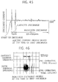
- Figure 46 shows the difference of electric wave form between them at the time of induction discharge. Al 2 O 3 + 60wt%CuO is used as thermal spraying material.
- the thermal sprayed layer has the porous part, much amount of micro discharge is generated between thermal spraying materials at the time of discharge, and relatively large induction discharge current continuously flows for a long time.
- the pulse noise caused by induction discharge current is input into the radio, and the PNL function repeats ON/OFF action of the gate for a long time. Therefore, the pulse noise input from the antenna of the radio is cut off, but the radio noise due to the repeated ON/OFF action of the gate in PNL circuit is generated.
- the PNL function repeats ON/OFF action of the gate about 50 times to firmly generate the radio noise.
- the porous part in the thermal sprayed layer results from the method for thermal spraying. Namely, in the process for thermal spraying on the surface of the rotor electrode faced to the opposite electrode, thermal spraying is performed in the direction perpendicular to the surface. At this time, the thermal spraying materials are adhered to the surface which is perpendicular to the thermal spraying direction, and also to the surface which is horizontal to the thermal spraying direction. Therefore, thick thermal spraying layer is formed on the surface which is perpendicular to the thermal spraying direction, and the porous thermal spraying layer is formed on the surface which is horizontal to the thermal spraying direction.
- the electrode substrate When discharge is generated at the portion of the electrode substrate which is near the boundary portion between the electrode substrate and the resistive material layer, the electrode substrate is fused by heat at the time of discharge since the electrode substrate comprises metal materials having lower fusing point than that of ceramics. Inventors have found that the temperature at the time of discharge reaches about 1300 to 1500°C sectionally. As a result, when the electrode had been used for a long time, a concave portion is formed at the portion of the electrode substrate which is near the boundary portion between the electrode substrate and the resistive material layer due to fused loss, and discharge is generated at the bottom of the concave portion. Then, discharge is hard to occur, or micro discharge is frequently occurred and relatively large induction discharge current continuously flows since the discharge passage becomes complicated. Therefore, noise electric is increased.
- a first object of the present invention is to further prevent noise electric wave by means of improvement of electrode.
- a second object of the present invention is to decrease the radio noise caused by the existence of the porous portion at the layer (thermal sprayed layer) for preventing noise electric wave of the electrode.
- a third object of the present invention is to prevent the formation of the concave portion at the portion of the electrode substrate which is near the boundary portion between the electrode substrate and the resistive material layer to effectively prevent the noise electric wave after the electrode had been used for a long time.
- the electrode for preventing noise electric wave and for solving the above first and second objects according to claim 1 comprises an electrode substrate; and a layer for preventing noise electric wave comprising thermal sprayed layer, being coated on the surface of the electrode substrate faced to an opposite electrode, and having the porosity of not more than 20%.
- the layer for preventing noise electric wave are not especially restricted, and high electric resistive material or electric insulating material can be used alone or in combinations.
- semi-conductive material can be used.
- the high electric resistive materials include CuO, Cr 2 O 3 , NiO, ZnO and so on;
- the electric insulating materials include Al 2 O 3 , SiO 2 , ZrO 2 , MgO and so on;
- the semi-conductive materials include FeO, Fe 2 O 3 , TiO 2 , ferrite and so on. It is preferable that oxides are used as materials of the layer for preventing noise electric wave in order to prevent oxidation deterioration due to discharge in the atmosphere.
- the electrode for preventing noise electric wave according to claim 1 can be manufactured by the following methods.
- the first method for producing the electrode according to claim 8 comprises a process for forming a layer for preventing noise electric wave comprising the thermal sprayed layer which is formed on one surface of the electrode substrate, and in which thermal spraying is performed in the direction perpendicular to the surface, and which has the porosity of not more than 20%; and a process for removing the thermal sprayed layer in which thermal spraying is performed on the other surface of the electrode substrate, and which has the porosity of more than 20%.
- the means for removing the thermal sprayed layer in which thermal spraying is performed on the other surface of the electrode substrate, and which has the porosity of more than 20% is not especially restricted.
- a grinding processing by means of grinder can be used.
- the second method for producing the electrode according to claim 9 comprises a process for laminating a number of electrode substrates; a process for forming the layer for preventing noise electric wave comprising the thermal sprayed layer which is formed on each edge surface of each electrode substrate, and in which thermal spraying is performed in the direction perpendicular to each edge surface, and which has the porosity of not more than 20%; and a process for separating the layer for preventing noise electric wave along a dividing line of each electrode substrate.
- the third method for producing the electrode according to claim 10 comprises a process for laminating a number of electrode substrates having a spacer therebetween in which edge portion of each spacer is projected from the edge surface of each electrode substrate by the predetermined length; a process for forming the layer for preventing noise electric wave comprising the thermal sprayed layer which is formed on each edge surface of each electrode substrate, and in which thermal spraying is performed in the direction perpendicular to each edge surface in such a manner that the thickness of the thermal sprayed layer is thinner than the above predetermined length, and which has the porosity of not more than 20%; and a process for removing the layer for preventing noise electric wave from each spacer.
- the fourth method for producing the electrode according to claim 11 comprises a process for laminating a number of electrode substrates; a process for forming the substrate thermal sprayed layer which is formed on each edge surface of each electrode substrate, and in which thermal spraying is performed in the direction perpendicular to each edge surface; a process for separating the substrate thermal sprayed layer along a dividing line of each electrode substrate; a process for re-laminating each electrode substrate coated with the substrate thermal sprayed layer; a process for forming the layer for preventing noise electric wave comprising the thermal sprayed layer which is coated on the substrate thermal sprayed layer formed on each edge surface of each electrode substrate, and in which thermal spraying is performed in the direction perpendicular to each edge surface of re-laminating electrode substrate, and which has the porosity of not more than 20%; and a process for separating the layer for preventing noise electric wave along a dividing line of each electrode substrate.
- the layer for preventing noise electric wave is made a notch by cutter or grinder for cutter to be separated.
- the fifth method for producing electrode according to claim 12 comprises a process for laminating a number of electrode substrates; a process for forming the layer for preventing noise electric wave comprising the thermal sprayed layer which is formed on each edge surface of each electrode substrate, and in which thermal spraying is performed in the direction perpendicular to each edge surface in such a manner that the electrode substrate is swung in order to repeat relative displacement between the two edge surfaces of two neighboring electrode substrates, and which has the porosity of not more than 20%.
- a number of electrode substrates are laminated in such a manner that each edge surface of each electrode substrate faced to the opposite electrode is exposed on the same surface because it is necessary to form the layer for preventing noise electric wave on the edge surface of the electrode substrate faced to the opposite electrode.
- the electrode substrates having wide area are laminated with each other since the thermal spraying materials are not adhered to the surface of the electrode substrate which is horizontal to the thermal spraying direction.
- the edge surface of the electrode substrates is rectangular form, it is preferable that the electrode substrates are laminated with each other in such a manner that the surface having long edge is overlapped with the other surface having long edge. It is more preferable that the electrode substrate is laminated with each other not only in one direction but also in two crossing directions in order that the thermal spraying materials are not adhered to the surface which is horizontal to the thermal spraying direction.
- the sixth method for producing the electrode according to claim 13 comprises a process for forming the layer for preventing noise electric wave comprising the thermal sprayed layer which is formed on one surface of long-shaped electrode substrate, and in which thermal spraying is performed in the direction perpendicular to the surface and which has the porosity of not more than 20%; and a process for separating the long-shaped electrode substrates into many pieces.
- the porous thermal sprayed layer in which the thermal spraying materials are adhered to the surface which is horizontal to the thermal spraying direction is removed by grinding processing or fused by high density energy to be densified as mentioned thereafter.
- the seventh method for producing the electrode according to claim 14 comprises a process for forming a layer for preventing noise electric wave comprising the thermal sprayed layer which is formed on one surface of the electrode substrate, and in which thermal spraying is performed in the direction perpendicular to the surface, and which has the porosity of not more than 20%; and a process for fusing the thermal sprayed layer in which thermal spraying is performed on the other surface of the electrode substrate, and which has the porosity of more than 20% by means of high density energy to be densified.
- the thermal spraying condition is not especially restricted if only the porosity of the thermal sprayed layer is not more than 20%.
- the electrode for preventing noise electric wave for solving the above first and third objects according to claim 2 preferably comprises a high-fusing conductive material layer which is formed on the surface of the substrate faced to the opposite electrode, and which has the resistivity of not more than 10 4 ohm centimeters, the fusing point of not less than 2000°C, and the thickness of not more than 30 micron seconds; and not less than one resisting material layer which is coated on the surface of the high-fusing conductive material layer faced to the opposite electrode.
- the discharge portion is moved to the side of the substrate.
- the concave portion is generated at the portion of the substrate which is near the boundary portion between the substrate and the high-fusing conductive material layer due to fused loss so that the performance is deteriorated. It is defined that the resistivity is always measured at the temperature of 20°C.
- the fusing point of the high-fusing conductive material layer is less than 2000°C, it is possible that the performance is deteriorated due to fused loss of the high-fusing conductive material layer itself. Furthermore, when the thickness of the high-fusing conductive material layer is less than 30 microns, the effect of the high-fusing conductive material layer cannot be obtained, and the heat from the discharge portion is moved to the substrate. Therefore, the concave portion is generated at the portion of the substrate which is near the boundary portion between the substrate and the high-fusing conductive material layer due to fused loss.
- the high-fusing conductive material layer comprises not less than one kind of materials consisting of Mo (having the resistivity of 5.7 x 10 -6 ohm centimeters, and the fusing point of 2622°C), Ta (having the resistivity of 13.5 x 10 -6 ohm centimeters and the fusing point of 2850°C), W (having the resistivity of 5.5 x 10 -6 ohm centimeters and the fusing point of 3382°C), Cr 2 O 3 (having the resistivity of 10 to 10 2 ohm centimeters and the fusing point of 2270°C) and CeO 2 (having the resistivity of 10 3 ohm centimeters and the fusing point of 2660°C).
- Mo having the resistivity of 5.7 x 10 -6 ohm centimeters, and the fusing point of 2622°C
- Ta having the resistivity of 13.5 x 10 -6 ohm centimeters and the
- the substrate comprises copper or copper alloy.
- the substrate comprises copper or copper alloy having high heat conductivity so that outgoing radiation is promoted, thereby preventing the substrate from being fused and damaged.
- the resisting material layer comprises an insulator of Al 2 O 3 , SiO 2 , ZrO 2 , MgO and the like, or a mixture of the insulator and a resistor of CuO, Cr 2 O 3 , NiO, ZnO, TiO 2 and the like.
- the electrode for preventing noise electric wave for solving the above first and third objects according to claim 5 preferably comprises a resisting material layer which is coated on the surface of the substrate faced to the opposite electrode.
- the substrate has a covering portion which is covered on the outer periphery of the resisting material layer and is located at the connecting portion between the substrate and the resisting material layer.
- the shape of the covering portion of the substrate is circular form in order to cover the whole periphery of the resisting material layer.
- the sectional form of the electrode is rectangular form in which the length of the long edge is remarkably longer than the length of the short edge, the covering portion can cover only the surfaces having wide area of the outer periphery of the resisting material layer.
- the thickness of the covering portion of the substrate is not more than 0.34mm.
- the thickness of the covering portion is more than 0.34mm, the covering portion is fused and damaged by the heat at the time of discharge. At the same time, the concave portion generated at the covering portion becomes deep, and noise electric wave becomes increasing.
- the length of the covering portion of the substrate is determined in accordance with the endurance travel distance, but it is preferable that the length of the covering portion is not less than 0.1mm.
- the length of the covering portion is shorter than 0.1mm, the covering portion is fused and damaged to be small. As a result, the discharge portion is generated from the substrate except the covering portion at the earlier stage so that the required performance cannot be obtained.
- the material of the resisting material layer is the same as those of the resisting material layer in the electrode for preventing noise electric wave according to claim 2.
- the layer for preventing noise electric wave comprising thermal sprayed layer is coated on the surface of the electrode substrate faced to the opposite electrode and has the porosity of not more than 20%. Therefore, the generation of the micro discharge at the porous portion of the thermal sprayed layer, which induces the induction discharge current having comparatively high absolute value level of the current value at the time of discharge to flow for a long time, can be controlled.
- the layer for preventing noise electric wave comprising the thermal sprayed layer and having the porosity of not more than 20% is confirmly formed only on the surface of the electrode substrate faced to the opposite electrode, it is possible to provide the electrode for preventing noise electric wave which can firmly prevent the generation of the micro discharge at the porous portion of the thermal sprayed layer.
- the second to fifth methods for producing the electrode according to the present invention since thermal spraying is performed at each edge surface of a number of laminated electrode substrates, it is possible to prevent the formation of the porous thermal sprayed layer at least on the overlapping surface made by two neighboring electrode substrates. At the same time, it is possible to manufacture many electrodes productively.
- the edge portion of each spacer located between laminated electrode substrates is projected from the edge surface of each electrode substrate by the predetermined length, and at the same time, thermal spraying is performed in such a manner that the thickness of the thermal sprayed layer is thinner than the above predetermined length.
- the substrate thermal spraying layer formed on the edge surface of each of the laminated electrode substrate is separated along a dividing line of electrode substrate, and then each electrode substrate is re-laminated. After that, the layer for preventing noise electric wave is formed on the separated substrate thermal spraying layer.
- a breaking portion of the substrate thermal spraying layer is the stress concentration point. Therefore, the layer for preventing noise electric wave is easily and firmly separated by the breaking portion.
- the fifth method for producing the electrode according to the present invention thermal spraying is performed, and at the same time, the electrode substrate is swung in order to repeat relative displacement between two edge surfaces of two neighboring electrode substrates.
- the layer for preventing noise electric wave formed on each electrode substrate is not adhered to each other. Therefore, it is possible to omit the process for separating the layer for preventing noise electric wave, and to prevent coming-off of the layer in the process for separating the layer.
- the layer for preventing noise electric wave is formed on one surface of long-shaped electrode substrate, and then the layer for preventing noise electric wave is cut into many pieces. Therefore, it is possible to prevent the formation of the porous thermal sprayed layer at least on the cut surface of each electrode substrate, and to manufacture many electrodes productively. Furthermore, it is possible to prevent coming-off or slippage of the layer since the layer for preventing noise electric wave is cut by machining.
- the porous thermal sprayed layer formed on the surface of the electrode substrate which is horizontal to the thermal spraying direction is fused by high density energy to be densified, and the porous portion of the thermal sprayed layer is firmly omitted. Therefore, it is possible to provide the electrode for preventing noise electric wave which can firmly prevent the generation of the micro discharge at the porous portion of the thermal sprayed layer.
- the high-fusing conductive material layer having special resistivity, fusing point and thickness exists between the substrate and the resisting material layer.
- the substrate having comparatively low fusing point is hardly fused and damaged by the heat at the time of discharge. Therefore, it is possible to prevent the formation of the concave portion which causes the increase in noise electric wave on the surface of the substrate.
- the high-fusing conductive material layer has high fusing point, the high-fusing conductive material is hardly fused and damaged by the heat, and the concave portion is hardly formed on the high-fusing conductive material layer.
- the substrate comprises copper or copper alloy having high heat conductivity
- the radiation effect from the substrate can be obtained since copper or copper alloy has high heat conductivity. Therefore, it is possible to control the concentration of the high density energy due to discharge at the high-fusing conductive material layer, and to decrease the possibility that the high-fusing conductive material layer is fused and damaged.
- the substrate has the covering portion which is covered on the outer periphery of the resisting material layer and is located at the connecting portion between the substrate and the resisting material layer.
- the covering portion At the portion of the covering portion which is near a boundary portion between the tip portion of the covering portion and the resisting material layer, discharge is generated.
- the covering portion is fused and damaged by the heat at the time of discharge, but the resisting material layer located at the lower surface of the covering portion is less fused and damaged since the resisting material has higher fusing point than that of the base material. Therefore, the damage of fused loss which causes the increase in noise electric wave is checked by the thickness of the covering portion, and the concave portion is hardly formed at the resisting material layer.
- the coating portion of the substrate is not less than 0.1mm, it is possible to extend the period that discharge is generated from the substrate except the coating portion which becomes gradually small. Therefore, it is possible to improve the durability.
- FIG. 2 is a whole schematic diagram of this electrode.
- the distributor comprises a rotor 1 which is rotatable at high speed, a rotor electrode 2 which is installed on the rotor 1 and a side electrode 3 which is opposite to the tip of the rotor electrode 2 with the clearance therebetween.
- FIG. 1 is a cross-sectional view for showing the rotor electrode 2 according to the Embodiment 1.
- the rotor electrode 2 comprises a substrate 20 made of brass, a substrate layer 21 formed on the surface of the substrate 20, a first layer 22 formed and coated on the surface of the substrate layer 21 and a second layer 23 formed and coated on the surface of the first layer 22.
- the substrate layer 21 is formed in such a manner that the first layer 22 is firmly adhered to the substrate 20 by thermal spraying.
- the substrate layer 21 is made of Ni-5%Al alloy and has the thickness of 100 microns.
- the substrate layer 21 is formed by plasma spraying method.
- the first layer 22 is made of CuO as oxide resistor and has the thickness of 200 microns.
- the resistivity value R 1 of the first layer 22 is in the range of 10 3 to 10 4 ohm centimeters.
- the second layer 23 is made of BaO as oxide resistor and has the thickness of 200 microns.
- the resistivity value R 2 of the second layer 23 is in the range of 10 9 to 10 10 ohm centimeters. Therefore, R 2 is larger than R 1 .
- Both the first layer 22 and the second layer 23 are formed by plasma spraying method.
- An electrode according to Comparative Example 1 comprises only a substrate 20.
- An electrode according to Comparative Example 2 has the same construction as that of the Embodiment 1 except that the second layer 23 is not existed.
- An electrode according to Comparative Example 3 has the same construction as that of the Embodiment 1 except that the first layer 22 formed on the surface of the substrate layer 21 is made of BaO and has the thickness of 200 microns, and that the second layer 23 is not existed.
- An electrode according to Comparative Example 4 has the same construction as that of the Embodiment 1 except that the first layer 22 formed on the surface of the substrate layer 21 is made of BaO and has the thickness of 200 microns, and that the second layer 23 is made of CuO and has the thickness of 200 microns. In this case, the resistivity value R 2 of the second layer 23 is smaller than the resistivity value R 1 of the first layer 22.
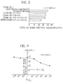
- Figure 3 shows the result of measuring the level of noise electric wave at the time of discharge concerning each electrode.
- the electrode according to the Embodiment 1 shows the most excellent effect for preventing noise electric wave.
- Comparative Example 4 when the first layer 22 and the second layer 23 in the Embodiment 1 are exchanged with each other, there is no effect for preventing noise electric wave.
- Figure 4 shows the change of the level of noise electric wave when the ratio of R 2 to R 1 (R 2 / R 1 ) is variously changed. As seen from Figure 4, when R 1 is larger than or equal to R 2 , there is no effect for preventing noise electric wave. Furthermore, when R 2 is larger than R 1 , there is remarkable effect for preventing noise electric wave.
- An electrode according to the Embodiment 2 has the same construction as that of the Embodiment 1 except that the construction of the first layer 22 and the second layer 23 is different.
- the first layer 22 is made of the mixture comprising Al 2 O 3 as oxide dielectric substance and CuO as oxide resistor, and the weight ratio of Al 2 O 3 to CuO is 4 : 6.
- the first layer 22 has the thickness of 400 microns, and the resistivity value is in the range of 10 4 to 10 6 ohm centimeters.
- the second layer 23 is made of only Al 2 O 3 as oxide dielectric substance.
- the second layer 23 has the thickness of 50 microns, and the resistivity value is 10 14 ohm centimeters.
- the second layer 23 has the larger resistivity than that of the first layer 22.
- Both the first layer 22 and the second layer 23 are formed by plasma spraying method which is the same method as that in the Embodiment 1.
- An electrode according to Comparative Example 1 comprises only a substrate 20.
- An electrode according to Comparative Example 5 has the same construction as that of the Embodiment 2 except that the second layer 23 is not existed.
- An electrode according to Comparative Example 6 has the same construction as that of the Embodiment 1 except that an insulation layer is formed on the surface of the substrate layer 21 in order to propagate electric power by use of creeping discharge.
- the insulation layer is made of Al 2 O 3 and has the thickness of 400 microns.
- both the discharge voltage and noise electric current of the Embodiment 2 are controlled to be low. As a result, noise electric field intensity is remarkably decreased. As compared with Comparative Examples 5 and 6, the electrode of the Embodiment 2 has about 2.5 to 3 times effect for decreasing noise electric wave.
- an electrode according to the Embodiment 3 has the same construction as that of the Embodiment 1 except that the first layer 22 is made of electromelting grinding material such as Al 2 O 3 -13%TiO 2 (in case of not more than 44%TiO 2 , it exists as Al 2 TiO 5 and Al 2 O 3 ) and has the thickness of 20 microns, and that the second layer is made of Al 2 O 3 and has the thickness of 50 microns.
- the first layer 22 is made of electromelting grinding material such as Al 2 O 3 -13%TiO 2 (in case of not more than 44%TiO 2 , it exists as Al 2 TiO 5 and Al 2 O 3 ) and has the thickness of 20 microns
- the second layer is made of Al 2 O 3 and has the thickness of 50 microns.
- the electromelting grinding material comprising Al 2 O 3 -13%TiO 2 is now put on the market, and it is excellent in its uniformity of dispersion and the cost.
- the electromelting grinding material is used as the first layer, it is possible to manufacture the electrode for preventing noise electric wave having excellent performance inexpensively.
- An electrode according to the Embodiment 4 has the same construction as that of the Embodiment 3 except that the thickness of the first layer 22 is 70 microns.
- An electrode according to the Embodiment 5 has the same construction as that of the Embodiment 3 except that the thickness of the first layer 22 is 100 microns.
- An electrode according to the Embodiment 6 has the same construction as that of the Embodiment 3 except that the thickness of the first layer 22 is 200 microns.
- An electrode according to the Embodiment 7 has the same construction as that of the Embodiment 3 except that the thickness of the first layer 22 is 800 microns.
- An electrode according to the Embodiment 8 has the same construction as that of the Embodiment 3 except that the thickness of the first layer 22 is 400 microns, and that the thickness of the second layer 23 is 20 microns.
- An electrode according to the Embodiment 9 has the same construction as that of the Embodiment 3 except that the thickness of the first layer 22 is 400 microns.
- An electrode according to the Embodiment 10 has the same construction as that of the Embodiment 3 except that the thickness of the first layer 22 is 400 microns, and that the thickness of the second layer 23 is 100 microns.
- An electrode according to the Embodiment 11 has the same construction as that of the Embodiment 3 except that the thickness of the first layer 22 is 400 microns, and that the thickness of the second layer 23 is 200 microns.
- An electrode according to the Embodiment 12 has the same construction as that of the Embodiment 3 except that the thickness of the first layer 22 is 400 microns, and that the thickness of the second layer 23 is 400 microns.
- An electrode according to Comparative Example 1 comprises only a substrate 20.
- An electrode according to the Embodiment 13 has the same construction as that of the Embodiment 3 except that the first layer 22 is made of the mixture comprising Al 2 O 3 and CuO (the weight ratio of Al 2 O 3 to CuO being 4 to 6) and has the thickness of 400 microns, and that the thickness of the second layer 23 is 100 microns.
- An electrode according to the Embodiment 14 has the same construction as that of the Embodiment 3 except that the first layer 22 is made of the mixture comprising Al 2 O 3 and CuO (the weight ratio of Al 2 O 3 to CuO being 4 to 6) and has the thickness of 400 microns, and that the thickness of the second layer 23 is 200 microns.
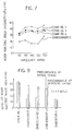
- the electrode according to the Embodiment 3 shows the low level of noise electric wave at the initial stage and at 24 hours later.
- the electrode according to the Embodiments 2 and 13 shows low level of noise electric wave at the initial stage, but noise electric wave becomes increasing at 24 hours later. This is caused by the generation of pin hole.
- the second layer 23 is made of only Al 2 O 3 as oxide dielectric substance, pin hole is generated under the condition that CuO having comparatively low fusing point is included in the first layer 22.
- the thickness of the first layer 22 is preferably not less than 0.1 mm, more preferably, not less than 0.2mm.
- the thickness of the second layer 23 is preferably not more than 0.1mm, more preferably, not more than 0.05mm.
- An electrode according to the Embodiment 15 has the same construction as that of the Embodiment 2 except that the second layer 23 is made of electromelting grinding material (Al 2 O 3 -2.3%TiO 2 ) as semi-conductive alumina and has the thickness of 50 microns.
- the second layer 23 is made of electromelting grinding material (Al 2 O 3 -2.3%TiO 2 ) as semi-conductive alumina and has the thickness of 50 microns.
- An electrode according to the Embodiment 16 has the same construction as that of the Embodiment 15 except that the amount of TiO 2 in the second layer 23 is 5%.
- An electrode according to the Embodiment 17 has the same construction as that of the Embodiment 15 except that the thickness of the first layer 22 is 20 microns, and that the amount of TiO 2 in the second layer 23 is 13%.
- An electrode according to the Embodiment 18 has the same construction as that of the Embodiment 15 except that the thickness of the first layer 22 is 70 microns, and that the amount of TiO 2 in the second layer 23 is 13%.
- An electrode according to the Embodiment 19 has the same construction as that of the Embodiment 15 except that the thickness of the first layer 22 is 100 microns, and that the amount of TiO 2 in the second layer 23 is 13%.
- An electrode according to the Embodiment 20 has the same construction as that of the Embodiment 15 except that the amount of TiO 2 in the second layer 23 is 13%.
- An electrode according to the Embodiment 21 has the same construction as that of the Embodiment 15 except that the thickness of the first layer 22 is 800 microns, and that the amount of TiO 2 in the second layer 23 is 13%.
- An electrode according to the Embodiment 22 has the same construction as that of the Embodiment 15 except that the amount of TiO 2 in the second layer 23 is 30%.
- An electrode according to the Embodiment 23 has the same construction as that of the Embodiment 15 except that the amount of TiO 2 in the second layer 23 is 44%.
- An electrode according to Comparative Example 7 has the same construction as that of the Embodiment 15 except that the second layer is made of 99%TiO 2 .
- An electrode according to Comparative Example 1 comprises only a substrate 20.
- An electrode according to the Embodiment 2 has the same construction as that of the Embodiment 1 except that the construction of the first layer 22 and the second layer 23 is different.
- the first layer 22 is made of the mixture comprising Al 2 O 3 as oxide dielectric substance and CuO as oxide resistor, and the weight ratio of Al 2 O 3 to CuO is 4 : 6.
- the first layer 22 has the thickness of 400 microns, and the direct current resistance value is in the range of 10 4 to 10 6 ohm centimeters.
- the second layer 23 is made of only Al 2 O 3 as oxide dielectric substance.
- the second layer 23 has the thickness of 50 microns, and the direct current resistance value is 10 14 ohm centimeters.
- the direct current resistance value is measured instead of the resistivity, but the second layer 23 has the larger resistivity than that of the first layer 22.
- An electrode according to the Embodiment 13 has the same construction as that of the Embodiment 2 except that the thickness of the second layer 23 is 100 microns.
- An electrode according to the Embodiment 14 has the same construction as that of the Embodiment 2 except that the thickness of the second layer 23 is 200 microns.
- An electrode according to the Embodiment 25 has the same construction as that of the Embodiment 2 except that the thickness of the second layer 23 is 20 microns.
- the electrode according to the Embodiment 20 shows the low level of noise electric wave at the initial stage and at 24 hours later.
- the electrode according to the Embodiments 2, 13 and 25 shows low level of noise electric wave at the initial stage, but noise electric wave becomes increasing at 24 hours later. This is caused by the generation of pin hole.
- the first layer 22 includes CuO having comparatively low fusing point, pin hole is hardly generated when the second layer 23 is made of Al 2 O 3 as oxide dielectric substance and TiO 2 as oxide resistor.
- the Embodiment 14 no pin hole is generated and noise electric wave shows the same level at the initial stage and at 24 hours later. However, the level of noise electric wave is high since the thickness of the second layer 23 is thick. As seen from Figures 13 and 14, there is an appropriate thickness of the first layer 22 and an appropriate added amount of TiO 2 for preventing noise electric wave.
- the added amount of TiO 2 is preferably in the range of 5 to 44%, more preferably, in the range of 5 to 22%.
- the thickness of the first layer is not less than 0.1mm, more preferably, not less than 0.4mm.
- the distributor according to the Fifth Preferred Embodiment comprises a rotor 1 which is rotatable at high speed, a T-shaped and planar rotor electrode 2 which is disposed at the rotor 1, and a side electrode 3 which is faced to the tip of the rotor electrode 2 with the clearance therebetween.
- a layer 2a for preventing noise electric wave comprising a thermal sprayed layer which is coated by thermal spraying is formed on the edge surface of the rotor electrode 2 which is faced to the side electrode 3.
- a rotor electrode 2 as the electrode for preventing noise electric wave is manufactured by the first method according to claim 7.
- the rotor electrode 2 according to the Embodiment 26 is made of brass having the thickness of 1.6mm.
- the rotor electrode 2 comprises an electrode substrate 20 which has two stepped portions 20a and 20a having each depth of about 1.2mm and an edge surface 24, and a layer 2a for preventing noise electric wave comprising a thermal sprayed layer which is coated on the edge surface 24 by thermal spraying.
- the layer 2a for preventing noise electric wave comprises 60wt% of CuO and 40wt% of Al 2 O 3 , and it has the porosity of 5% and the thickness of 400 microns.
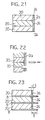
- the rotor electrode 2 is manufactured as follows. As shown in Figure 17, a number of the above electrode substrates 20 are laminated in such a manner that the edge surface 24 is uniform surface, and the laminated electrode substrates 20 are set in a tool (not shown). The tool covers the right and left side surfaces of each laminated electrode substrate 20, the upper surface of the electrode substrate 20 at the top and the lower surface of the electrode substrate 20 at the bottom. Then, Al 2 O 3 -60wt%CuO material is thermal sprayed by plasma method in the direction which is perpendicular to the edge surface 24 of each electrode 20.
- the thermal spraying by plasma method is performed under the condition that the porosity is set to be 5%, the voltage is 500V, the current is 75A, the thermal spraying distance is 100mm and the amount of powder supply is 40g/minute.
- the thermal sprayed layer formed on the stepped portion 20a of each electrode substrate 20 is not brought into contact with each other.
- the tool is removed and each electrode substrate is disassembled.
- a grinding machining is performed in such a manner that a grinder is brought into contact with the stepped portion 20a of each electrode substrate 20.
- the thermal sprayed layer formed on the stepped portion 20a is removed and the rotor electrode 2 according to the Embodiment 26 is completed.
- the layer 2a for preventing noise electric wave comprising the thermal sprayed layer having the porosity of not more than 20% is firmly formed only on the edge surface 24 of the electrode substrate 20. Therefore, it is possible to provide the electrode for preventing noise electric wave which can firmly prevent the generation of micro discharge at the porous portion of the thermal sprayed layer.
- the thermal spraying distance at the time of thermal spraying by plasma method is changed, and the porosity of the layer 2a for preventing noise electric wave is variously changed in the range of 5 to 50%, thereby manufacturing each rotor electrode.
- Concerning these rotor electrodes and the above completed rotor electrode 2 were measured.
- the PNL operating time was measured by the turbulent time which is caused by that the positive magnetic wave is introduced from the radio antenna.
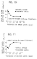
- the radiation electric field intensity was measured by vehicles. The result is shown in Figure 18.
- the PNL operating time becomes short as the porosity of the layer 2a for preventing noise electric wave is decreased.
- the decreasing rate becomes almost constant.
- the radiation electric field intensity maintains a certain value without receiving the influence of the porosity of the layer 2a for preventing noise electric wave.
- the PNL operating time is drastically decreased. Therefore, it is possible to decrease the radio noise without decreasing the effect for preventing noise electric wave.
- the amount of grinding of the grinding machining is controlled, and the thickness l of the thermal sprayed layer formed on the stepped portion 20a of the electrode substrate 20 is variously changed in the range of 0 to 200 microns, thereby manufacturing each rotor electrode. Concerning these rotor electrodes and the above completed rotor electrode 2, PNL operating time and radiation electric field intensity were measured. The result is shown in Figure 19. As shown in Figure 20, the thickness l of the thermal sprayed layer formed on the stepped portion 20a of the electrode substrate 20 is the maximum thickness, and the porosity of the thermal sprayed layer is about 50%. The thermal sprayed layer formed on the edge surface 24 of the electrode substrate has the thickness L of 400 microns, and the porosity of about 5%.
- the PNL operating time becomes short as the thickness of the porous thermal sprayed layer is decreased.
- the PNL operating time becomes the shortest.
- the radiation electric field intensity maintains a certain value without receiving the influence of thickness of the porous thermal sprayed layer.
- the PNL operating time is decreased. Therefore, it is possible to decrease the radio noise without decreasing the effect for preventing noise electric wave.
- a rotor electrode 2 as the electrode for preventing noise electric wave is manufactured by the second method according to claim 8.
- the materials for the electrode substrate 20 and the layer 2a for preventing noise electric wave are the same as those of the Embodiment 26, and the layer 2a for preventing noise electric wave has the porosity of 5% and the thickness of 400 microns.
- a number of the electrode substrates 20 having the same thickness (1.6mm) each other are laminated in such a manner that the edge surface 24 is uniform surface, and the laminated electrode substrates 20 are set in a tool (not shown). Then, Al 2 O 3 -60wt%CuO material is thermal sprayed by plasma method in the direction which is perpendicular to the edge surface 24 of each electrode 20. The thermal spraying by plasma method is performed under the same condition as that of the Embodiment 26. After the tool is removed, the layer 2a for preventing noise electric wave is separated along a dividing line of each electrode substrate 20. Thus, the rotor electrode 2 according to the Embodiment 27 is completed.
- the thermal spraying is performed to each edge surface 24 of many laminated electrode substrates 20. Therefore, it is possible to prevent the formation of the porous thermal sprayed layer at least on the overlapping surface of the neighboring electrode substrates 20. Furthermore, it is possible to manufacture many electrodes productively.
- the thickness of the layer 2a is not more than 500 microns.
- a rotor electrode 2 is manufactured by the same method and same manners as those of the Embodiment 27 except the following.
- the layer 2a for preventing noise electric wave and the electrode substrate 20 are made a notch along the overlapped portion of the electrode substrate 20 by grinder for cutter (the thickness of 0.5mm).
- the depth of the notch is twice as much as the thickness of the layer 2a for preventing noise electric wave. Therefore, it is possible to easily and firmly separate the layer 2a for preventing noise electric wave.
- a rotor electrode 2 as the electrode for preventing noise electric wave is manufactured by the third method according to claim 9.
- the materials for the electrode substrate 20 and the layer 2a for preventing noise electric wave are the same as those of the Embodiment 26, and the layer 2a for preventing noise electric wave has the porosity of 5% and the thickness of 400 microns.
- a planar spacer 8 made of steel material having the thickness of 0.1mm is prepared. As shown in Figure 23, a number of the electrode substrates 20 having the same thickness (1.6mm) each other and a number of spacers 8 are laminated in such a manner that the edge surface 24 is uniform surface and that the tip of each spacer 8 is projected from the edge surface 24 of the electrode substrate 20 by 1.0mm, and the laminated electrode substrates 20 are set in a tool (not shown). The spacer 8 is disposed at the top and bottom edges in the laminated direction. Then, Al 2 O 3 -60wt%CuO material is thermal sprayed by plasma method in the direction which is perpendicular to the edge surface 24 of each electrode 20.
- the thermal spraying by plasma method is performed under the same condition as that of the Embodiment 26. After the tool is removed, the layer 2a for preventing noise electric wave is tore off from each spacer 8. Thus, the rotor electrode 2 according to the Embodiment 29 is completed.
- the layer 2a for preventing noise electric wave formed at the edge surface 24 of each electrode substrate 20 is previously separated by each spacer 8. Therefore, it is possible to control the coming-off of the layer at the time of separating the layer 2a for preventing noise electric wave.
- the thickness of the spacer 8 is not especially restricted. However, it is necessary that the length T of the spacer 8 projected from the edge surface 24 is longer than at least the thickness t of the layer 2a for preventing noise electric wave. It is preferable that the material of the spacer 8 is excellent in coming-off from the thermal sprayed material.
- a rotor electrode 2 as the electrode for preventing noise electric wave is manufactured by the fourth method according to claim 10.
- the materials for the electrode substrate 20 and the layer 2a for preventing noise electric wave are the same as those of the Embodiment 26, and the layer 2a for preventing noise electric wave has the porosity of 5% and the thickness of 400 microns.
- a number of the electrode substrates 20 having the same thickness (1.6mm) each other are laminated in such a manner that the edge surface 24 is uniform surface, and the laminated electrode substrates 20 are set in a tool (not shown). Then, Ni-5%Al alloy as the thermal spraying material is thermal sprayed in the direction which is perpendicular to the edge surface 24 of each electrode 20 to form a substrate thermal sprayed layer 2b having the thickness of 100 microns. After the tool is removed, the substrate thermal sprayed layer 2b is separated along a dividing line of each electrode substrate 20. Each electrode substrate 20 on which the substrate thermal sprayed layer 2b is formed is re-laminated, and the re-laminated electrode substrates 20 are set in the tool.
- Al 2 O 3 -60wt%CuO material is thermal sprayed by plasma method in the direction which is perpendicular to the edge surface 24 of each electrode 20.
- the thermal spraying by plasma method is performed under the same condition as that of the Embodiment 26.
- the layer 2a for preventing noise electric wave is separated along a dividing line of each electrode substrate 20.
- the rotor electrode 2 according to the Embodiment 30 is completed.
- a breaking portion of the substrate thermal sprayed layer 2b is stress concentration point. Since the breaking portion is determined as the starting point, it is possible to easily and firmly separate the layer 2a for preventing noise electric wave. Furthermore, the adhesion of the layer 2a for preventing noise electric wave to the electrode substrate 20 is improved by the substrate thermal sprayed layer 2b. Therefore, it is possible to control the coming-off of the layer at the time of separating the layer 2a for preventing noise electric wave.
- a rotor electrode 2 as the electrode for preventing noise electric wave is manufactured by the fifth method according to claim 11.
- the materials for the electrode substrate 20 and the layer 2a for preventing noise electric wave are the same as those of the Embodiment 26, and the layer 2a for preventing noise electric wave has the porosity of 5% and the thickness of 400 microns.
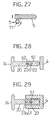
- an electrode substrate 20 having a key hole 23 with a key engaging portion 23a is prepared.
- a number of the electrode substrates 20 having the same thickness (1.6mm) each other are laminated, and set in a swing apparatus which mainly comprises a fixed tool 4, a swing tool 5, a motor 6 and a cam shaft 7 as follows.
- the swing tool 5 is brought into contact with a cam portion 71 of the cam shaft 7 which is connected with the motor 6, and it is swingable in the right and left directions (namely, in the direction vertical to the paper in Figure 26; or in the up and down directions in Figure 27) by the rotation of the cam shaft 7.
- the swing tool 5 has a bar portion 51 and a number of key portions 52.
- the bar portion 51 is inserted through the key hole 23 of each laminated electrode substrate 20, and the key portion 52 is engaged with the key engaging portion 23a of the key hole 23 of every other laminated electrode substrate 20.
- the right and left side surfaces is restricted their movement in the right and left directions by a regulated wall surface 41 of the fixed tool 4. Furthermore, concerning the laminated electrode substrates 20, the upper surface of the electrode substrate 20 at the top and the lower surface of the electrode substrate 20 at the bottom are respectively covered by an upper wall surface 42 and a lower wall surface of the fixed tool 4.
- the cam shaft 7 is rotated by driving the motor 6, and the swing tool 5 is swung. Then, Al 2 O 3 -60wt%CuO material is thermal sprayed by plasma method in the direction which is perpendicular to the edge surface 24 of each electrode 20 while swinging only the electrode substrate 20 in which the key portion 52 is engaged with the key engaging portion 23a of the key hole 23.
- the thermal spraying by plasma method is performed under the same condition as that of the Embodiment 26.
- the swing is performed under the condition that the swing frequency is 5Hz, and the swing amplitude is 700 microns.
- the formation speed of the thermal sprayed layer is 100 microns per second, the thickness of the thermal sprayed layer which is formed during 1 cycle of swing is 20 microns.
- the average particle diameter of the thermal spraying material powder is 22 microns. After the thermal spraying material is thermal sprayed, it becomes flat and the average particle diameter is 70 microns. Therefore, the value of s (the swing amplitude) to d (the particle diameter after thermal spraying) is 10.
- the swing apparatus is removed from each electrode substrate 20, and the rotor electrode 2 according to the Embodiment 31 is completed.
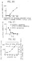
- the relationship between the swing speed and the fraction defective of the thermal sprayed layer is examined under the above condition.
- the fraction defective is defined as the coming-off of the thermal sprayed layer or the crack in the layer due to swing.
- the thickness of the thermal sprayed layer which is formed during 1 cycle of swing is used to judge whether the condition of the swing speed is good or not. The result is shown in Figure 30.
- a rotor electrode 2 as the electrode for preventing noise electric wave is manufactured by the sixth method according to claim 12.
- the materials for the electrode substrate 20 and the layer 2a for preventing noise electric wave are the same as those of the Embodiment 26, and the layer 2a for preventing noise electric wave has the porosity of 5% and the thickness of 400 microns.
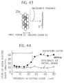
- a long-shaped electrode raw material having the same cross-sectional shape as that of the electrode substrate 20 is prepared. Then, Al 2 O 3 -60wt%CuO material is thermal sprayed by plasma method to one surface of the electrode raw material in the perpendicular direction. The thermal spraying by plasma method is performed under the same condition as that of the Embodiment 26. After that, the thermal sprayed electrode raw material is cut in the direction perpendicular to the thermal sprayed surface by grinder for cutter to be the electrode substrate 20 having a certain thickness. Thus, the rotor electrode 2 according to the Embodiment 32 is completed.
- Embodiment 32 it is possible to prevent the formation of the porous thermal sprayed layer at least on the cut surface of the separated electrode substrate 20. Furthermore, it is possible to manufacture many electrodes productively. Moreover, the layer 2a for preventing noise electric wave is separated by machining at the time of cutting. Therefore, it is possible to control the coming-off of the layer 2a or slippage at the cut surface.
- a rotor electrode 2 as the electrode for preventing noise electric wave is manufactured by the seventh method according to claim 13.
- the materials for the electrode substrate 20 and the layer 2a for preventing noise electric wave are the same as those of the Embodiment 26, and the layer 2a for preventing noise electric wave has the porosity of 5% and the thickness of 400 microns.
- a number of the electrode substrates 20 which has the same shape as that of the Embodiment 26 are laminated in such a manner that the edge surface 24 is uniform surface, and the laminated electrode substrates 20 are set in a tool (not shown).
- the tool maintains the base edge side of each laminated electrode substrate 20.
- the right and left side surfaces of each laminated electrode substrate 20, the upper surface of the electrode substrate 20 at the top and the lower surface of the electrode substrate 20 at the bottom are exposed at the tip side of each electrode substrate 20, namely, at the edge surface 24 on which thermal spraying is performed.
- Al 2 O 3 -60wt%CuO material is thermal sprayed by plasma method in the direction which is perpendicular to the edge surface 24 of each electrode 20.
- the thermal spraying by plasma method is performed under the same condition as that of the Embodiment 26. After that, the tool is removed and each electrode substrate is disassembled. The thermal sprayed layer formed on the surface of each electrode substrate 20 which is horizontal to the thermal spraying direction (the upper and lower surfaces and the right and left side surfaces of the stepped portion 20a) is fused and densified by laser irradiation. Thus, the rotor electrode 2 according to the Embodiment 33 is completed.
- the laser irradiation is performed under the condition that the laser output is 100W, the laser pulse is 10msec/pulse and 20pulse/second, and the irradiation traverse speed is 1cm/second.
- the porosity of the thermal sprayed layer before laser irradiation is about 50%, and the porosity of the thermal sprayed layer after laser irradiation is about 10%.
- the porous thermal sprayed layer formed on the surface of the electrode substrate 20 which is horizontal to the thermal spraying direction is densified by laser irradiation, and the porous portion of the thermal sprayed layer is firmly omitted. Therefore, it is possible to provide the electrode for preventing noise electric wave which can firmly prevent the generation of the micro discharge at the porous portion of the thermal sprayed layer.
- the laser output and the time for irradiation are changed, and the porosity of the thermal sprayed layer formed on the surface of the electrode substrate which is horizontal to the thermal spraying direction is variously changed, thereby manufacturing each rotor electrode.
- the PNL operating time becomes short as the porosity of the above thermal sprayed layer is decreased.
- the decreasing rate becomes almost constant.
- the radiation electric field intensity maintains a certain value without receiving the influence of the porosity of the thermal sprayed layer.
- the PNL operating time is drastically decreased. Therefore, it is possible to decrease the radio noise without decreasing the effect for preventing noise electric wave.
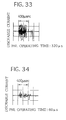
- Figure 33 shows the result of examining PNL operating time and the induced discharge wave form before the porous thermal sprayed layer is fused.
- Figure 34 shows the result of examining PNL operating time and the induced discharge wave form after the porous thermal sprayed layer is fused. As shown in Figures 33 and 34, it is possible to drastically decrease the PNL operating time and the radio noise.
- Embodiment 33 not only the laser irradiation but also the electron beam is used as the means for fusing the thermal sprayed layer which is formed on the surface of the electrode substrate which is horizontal to the thermal spraying direction.
- an electrode for preventing noise electric wave according to claim 14 is use as a rotor electrode 2.
- the rotor electrode 2 according to the Embodiment 34 comprises an electrode substrate 20 made of brass having the thickness of 1.6mm, a high-fusing conductive material layer 25 which is coated by thermal spraying on the surface of the electrode substrate 20 faced to a side electrode 3, a first resisting material layer 26 which is coated by thermal spraying on the surface of the high-fusing conductive material layer 25, and a second resisting material layer 27 which is coated by thermal spraying on the surface of the first resisting material layer 26.
- the high-fusing conductive material layer 25 is made of Mo having the resistivity of 5.7 x 10 -6 ohm centimeters and the fusing point of 2622°C.
- the thickness of the high-fusing conductive material layer 25 is 100 microns.
- the first resisting material layer 26 is made of Al 2 O 3 -13%TiO 2 .
- the thickness of the first resisting material layer 26 is 400 microns.
- the second resisting material layer 27 is made of Al 2 O 3 .
- the thickness of the second resisting material layer is 50 microns.
- the high-fusing conductive material layer 25, the first resisting material layer 26 and the second resisting material layer 27 are formed by Plasma thermal spraying method. After thermal spraying, the upper and lower surfaces of the electrode substrate 20 are ground, and the porous thermal sprayed layer formed on the upper and lower surfaces of the electrode substrate 20 is removed.
- the rotor electrode comprises an electrode substrate which is made of brass; a first resisting material layer (first layer) which is made of Al 2 O 3 -13%TiO 2 , and which is coated by thermal spraying on the surface of the electrode substrate, and which has the thickness of 400 microns; and a second resisting material layer (second layer) which is made of Al 2 O 3 , and which is coated by thermal spraying on the surface of the electrode substrate, and which has the thickness of 50 microns.
- first layer which is made of Al 2 O 3 -13%TiO 2
- second layer which is made of Al 2 O 3
- a rotor electrode is prepared.
- the rotor electrode is the same as that of the Embodiment 9 except that the electrode substrate is made of Mo.
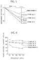
- the rotor electrode of the Embodiment 35 in which the electrode substrate is made of Mo having higher fusing point than that of brass has lower decreasing speed in performance for preventing noise electric wave than that of the Embodiment 9 in which the electrode substrate is made of brass.
- both of these rotor electrodes show the same deteriorated performance at last.
- the thickness of the high-fusing conductive material layer 25 for improving the durability of the performance for preventing noise electric wave.
- the thickness of the high-fusing conductive material layer 25 is less than 30 microns, the effect for improving the durability due to the high-fusing conductive material layer 25 cannot be satisfactorily achieved. Therefore, it is necessary that the thickness of the high-fusing conductive material layer 25 is not less than 30 microns, preferably, not less than 70 microns.
- the thickness is not more than 200 microns since coming-off of the layer is generated.
- an electrode for preventing noise electric wave according to claim 17 is use as a rotor electrode 2.
- the rotor electrode 2 according to the Embodiment 36 comprises an electrode substrate 20 made of brass, a first resisting material layer 26 which is coated by thermal spraying on the surface of the electrode substrate 20 faced to a side electrode, and a second resisting material layer 27 which is coated by thermal spraying on the surface of the first resisting material layer 26.
- the electrode substrate 20 has a covering portion 28 which is covered on the upper and lower surfaces of the first resisting material layer 26, and which is located at the connecting portion between the electrode substrate and the first resisting material layer 26.
- the thickness a of the covering portion is 0.2mm, and the length b of the covering portion is 0.5mm.
- the first resisting material layer 26 is made of Al 2 O 3 -13%TiO 2 .
- the thickness of the first resisting material layer 26 from the edge surface of the covering portion 28 is 400 microns.
- the second resisting material layer 27 is made of Al 2 O 3 .
- the thickness of the second resisting material layer 27 is 50 microns.
- the first resisting material layer 26 and the second resisting material layer 27 are formed by Plasma thermal spraying method on the electrode substrate 20 on which the covering portion 28 is previously formed. After thermal spraying, the upper and lower surfaces of the electrode substrate 20 are ground, and the porous thermal sprayed layer formed on the upper and lower surfaces of the electrode substrate 20 is removed. Therefore, the thickness of the electrode substrate 20 is 1.0mm.
- the rotor electrode comprises an electrode substrate with no covering portion 28 which is made of brass; a first resisting material layer (first layer) which is made of Al 2 O 3 -13%TiO 2 , and which is coated by thermal spraying on the surface of the electrode substrate, and which has the thickness of 400 microns; and a second resisting material layer (second layer) which is made of Al 2 O 3 , and which is coated by thermal spraying on the surface of the electrode substrate, and which has the thickness of 50 microns.
- first layer which is made of Al 2 O 3 -13%TiO 2
- second layer which is made of Al 2 O 3
- the performance for preventing noise electric wave becomes deteriorated to some extent until 100 hours. After that, it is possible to maintain almost constant performance, and this is acceptable as compared with the law regulating level. On the contrary, concerning the rotor electrode according to the Embodiment 9 with no covering portion 28, the performance for preventing noise electric wave becomes deteriorated to show the higher level than the law regulating level until 100 hours, and is further deteriorated until 400 hours.
- the thickness a of the covering portion 28 is not more than 0.34mm, more preferably, not more than 0.25mm.
- the thickness a of the covering portion 28 becomes too thin, it is preferable that the thickness is not less than 0.1mm since the speed for progressing fused loss becomes high.
- the length b of the covering portion 28 is not less than 0.1mm per 50000km of the travel distance of an automobile. Therefore, it is preferable that the length b of the covering portion 28 is not less than 0.1mm, more preferably, not less than 0.6mm.
- an electrode for preventing noise electric wave according to claim 5 is use as a rotor electrode 2.
- the rotor electrode 2 according to the Embodiment 37 comprises a substrate 20 made of brass, a substrate layer 21 formed on the surface of the substrate 20, a first layer 22 formed and coated on the surface of the substrate layer 21 and a second layer 23 formed on the surface of the first layer 22.
- the substrate layer 21 is formed in such a manner that the first layer 22 is firmly adhered to the substrate 20 by thermal spraying.
- the substrate layer 21 is made of Ni-5%Al alloy and has the thickness of 50 microns.
- the substrate layer 21 is formed by plasma spraying method.
- the first layer 22 is made of Al 2 TiO 5 -70wt%Al 2 O 3 and has the thickness of 400 microns.
- the first layer 22 is formed by plasma spraying method.
- the direct current resistance value R 1 of the first layer 22 is in the range of 10 9 ohm.
- the second layer 23 is formed by performing heat-oxidation treatment due to plasma flame on the surface of the first layer 22.
- the second layer 23 has the thickness of about 10 microns.
- the direct current resistance value R 2 of the second layer 23 is in the range of 10 10 ohm.
- Al 2 TiO 5 is changed from insulating material to resisting material since oxygen defect is generated by plasma spraying. After that, Al 2 TiO 5 is changed from resisting material to insulating material again because oxygen is supplied by oxidation treatment.
- the first layer 22 is coated on the surface of the substrate 20, and the second layer 23 is formed on the surface of the first layer 22 by performing oxidation treatment on the surface of the first layer 22. After that, the upper and lower surfaces of the electrode are polished, and a porous thermal sprayed layer formed on the upper and lower surfaces is removed. Thus, the rotor electrode 2 is completed.
- a first layer 22 is coated and formed on the surface of a substrate layer 21 of a substrate 20 by plasma spraying method in the same manner as that of the Embodiment 37.
- a second layer 23 is coated and formed on the surface of the first layer 22 by plasma spraying method.
- the second layer 23 is made of Al 2 O 3 and has the thickness of about 10 microns.
- a rotor electrode 2 is manufactured by the same method according to the Embodiment 38 except that the first layer 22 is made of TiO 2 -70wt%Al 2 O 3 and has the thickness of 400 microns.
- a rotor electrode 2 is manufactured by the same method according to the Embodiment 38 except that the first layer 22 is made of TiO 2 -15wt%Al 2 TiO 5 -70wt%Al 2 O 3 and has the thickness of 400 microns.
- a rotor electrode 2 according to Comparative Example 1 comprises only a substrate which is made of brass.
- a rotor electrode 2 is manufactured by the same method according to the Embodiment 37 except that only an insulation layer is formed on the surface of the substrate layer 21.
- the insulating layer is made of Al 2 O 3 (99.7%) and has the thickness of 400 microns.
- a rotor electrode 2 is manufactured by the same method according to the Embodiment 37 except that the first layer 22 is made of CuO-40wt%Al 2 O 3 and has the thickness of 400 microns, and the second layer 23 is not formed.
- a rotor electrode 2 is manufactured by the same method according to the Embodiment 39 except that the second layer 23 is not formed.
- a rotor electrode 2 is manufactured by the same method according to the Embodiment 40 except that the second layer 23 is not formed.
- each electrode according to the Embodiments 37 and 38 show the excellent effect for preventing noise electric wave not only at the initial stage but also at 500 hours later.
- discharge is generated from the boundary portion between the substrate 20 and the first layer 22.
- the discharge passage is extended toward the opposite electrode (cathode) 3 along the upper and lower surfaces and the tip surface of the electrode, and creeping discharge can be observed.
- metal oxide in the first layer 22 exists as composite oxide such as Al 2 TiO 5 , and it contributes to the effect for preventing noise electric wave.
- the component elements of Al 2 TiO 5 such as Ti and 0 exist as TiO 2 having low electric resistance
- the second layer 23 is broken, thereby generating discharge.
- the second layer 23 is fused and damaged. After that, discharge is generated from the tip surface of the second layer 23, and the effect for preventing noise electric wave is deteriorated.
- metal oxide in the first layer 22 exists as composite oxide such as Al 2 TiO 5
- the above discharge passage and the effect for preventing noise electric wave can be obtained since Al 2 TiO 5 shows higher electric resistance than that of TiO 2 .
- the second layer 23 exists as an insulation layer.
- a thermal sprayed layer is formed on the tip surface of the substrate 20 by plasma spraying method.
- the substrate 20 is made of brass, and the thermal sprayed layer is made of Al 2 TiO 5 and has the thickness of 0.4mm.
- the direct current resistance value of Al 2 TiO 5 was measured by an ammeter when the voltage of 100V was acted on a boundary portion between the upper surface of the substrate 20 and the tip surface of the thermal sprayed layer. As a result, the direct current resistance value was in the range of 1 x 10 6 to 1 x 10 7 ohm.
- the direct current resistance value of TiO 2 was 10 ohm
- Al 2 O 3 was 1 x 10 12 ohm.
- the thickness of the second layer 23 is more than 25 microns, there is no problem on the initial noise characteristics. However, the level of noise is radically increased at 500 hours later. The reason of this is as follows. When the thickness of the second layer 23 is more than 25 microns, impedance of whole electrode becomes high. So, heating energy becomes high at the place for generating discharge, and the local place is fused and damaged. Therefore, it is preferable that the thickness of the second layer 23 is not more than 25 microns. Since the second layer 23 is used for preventing the outflow of electron from oxide resistor of the first layer 22, it is no problem that the second layer 23 is thin.
- each electrode for preventing noise electric wave it is possible to prevent noise electric wave for a long time. As a result, other step for preventing noise electric wave such as a bonding wire is not required, so it is possible to decrease the cost and the manhour. Furthermore, since each electrode has the same noise level as that of a ceramic rotor electrode which is expensive, it is possible to use each electrode as a substitution for the ceramic rotor electrode. Therefore, it is possible to lower the cost remarkably.
- each electrode for preventing noise electric wave according to the present invention, the generation of relatively large induction discharge current which is caused by the micro discharge at the porous portion of the thermal sprayed layer can be controlled. As a result, it is possible to prevent the radio noise which is caused by the induction discharge current.
- the layer for preventing noise electric wave which comprises only a thermal sprayed layer having the porosity of not more than 20%.
- the second to fifth methods for producing the electrode according to the present invention since thermal spraying is performed at each edge surface of a number of laminated electrode substrates, it is possible to prevent the formation of the porous thermal sprayed layer at least on the overlapping surface made by two neighboring electrode substrates. At the same time, it is possible to manufacture many electrodes productively, and to lower the cost.
- each layer for preventing noise electric wave formed on each electrode substrate is previously separated by each spacer. Therefore, it is possible to control coming-off of the layer at the time of separating the layer for preventing noise electric wave, and to improve the quality.
- the fourth method for producing the electrode according to the present invention when the layer for preventing noise electric wave is separated along a dividing line of each electrode substrate, a breaking portion of a substrate thermal sprayed layer is used as a starting point. Therefore, it is possible to easily and firmly separate the layer for preventing noise electric wave, and to improve the quality.
- the layer for preventing noise electric wave formed on each electrode substrate is not adhered to each other.
- the layer for preventing noise electric wave is formed on one surface of long-shaped electrode substrate, and then the long-shaped electrode substrate is cut into many pieces. Therefore, it is possible to prevent the formation of the porous thermal sprayed layer at least on the cut surface of each electrode substrate, and to manufacture many electrodes productively, and to lower the cost. Furthermore, it is possible to prevent coming-off or slippage of the layer since the layer for preventing noise electric wave is separated by machining at the time of cutting.
- the portion for the discharge generation is moved from the substrate to the high-fusing conductive material layer. Therefore, it is possible to prevent the generation of fused loss which causes increase in noise electric wave.
- the substrate comprises copper or copper alloy having high heat conductivity.
- the substrate preferably has the covering portion which is covered on the resisting material layer. Therefore, the damage of fused loss which causes the increase in noise electric wave is checked by the thickness of the covering portion, and it is possible to improve the durability.
- each electrode for preventing noise electric wave since the above covering portion preferably has a certain dimension, it is possible to further improve the durability.
- the layer for preventing noise electric wave has the porosity of not more than 20%, it is possible to prevent the radio noise.
- the electrode for preventing noise electric wave according to the present invention in which the high-fusing conductive material layer exists between the substrate and the resisting material layer, it is possible to prevent the formation of the concave portion.
Landscapes
- Engineering & Computer Science (AREA)
- Chemical & Material Sciences (AREA)
- Combustion & Propulsion (AREA)
- Mechanical Engineering (AREA)
- General Engineering & Computer Science (AREA)
- Ignition Installations For Internal Combustion Engines (AREA)
- Shielding Devices Or Components To Electric Or Magnetic Fields (AREA)
- Coating By Spraying Or Casting (AREA)
- Surface Acoustic Wave Elements And Circuit Networks Thereof (AREA)
- Thermistors And Varistors (AREA)
Applications Claiming Priority (13)
| Application Number | Priority Date | Filing Date | Title |
|---|---|---|---|
| JP202662/93 | 1993-07-22 | ||
| JP20266293 | 1993-07-22 | ||
| JP20266293 | 1993-07-22 | ||
| JP29083593 | 1993-11-19 | ||
| JP29083593 | 1993-11-19 | ||
| JP290835/93 | 1993-11-19 | ||
| JP3126294 | 1994-03-01 | ||
| JP3126294 | 1994-03-01 | ||
| JP31262/94 | 1994-03-01 | ||
| JP15385794A JP3152068B2 (ja) | 1993-07-22 | 1994-07-05 | 雑音電波防止用電極及びその製造方法 |
| JP15385794 | 1994-07-05 | ||
| JP153857/94 | 1994-07-05 | ||
| EP94111444A EP0635637B1 (fr) | 1993-07-22 | 1994-07-21 | Electrode pour supprimer les ondes électriques de bruit parasite et procédé de fabrication de celle-ci |
Related Parent Applications (2)
| Application Number | Title | Priority Date | Filing Date |
|---|---|---|---|
| EP94111444.9 Division | 1994-07-21 | ||
| EP94111444A Division EP0635637B1 (fr) | 1993-07-22 | 1994-07-21 | Electrode pour supprimer les ondes électriques de bruit parasite et procédé de fabrication de celle-ci |
Publications (3)
| Publication Number | Publication Date |
|---|---|
| EP0793016A2 true EP0793016A2 (fr) | 1997-09-03 |
| EP0793016A3 EP0793016A3 (fr) | 1998-08-19 |
| EP0793016B1 EP0793016B1 (fr) | 2004-05-12 |
Family
ID=27459408
Family Applications (2)
| Application Number | Title | Priority Date | Filing Date |
|---|---|---|---|
| EP94111444A Expired - Lifetime EP0635637B1 (fr) | 1993-07-22 | 1994-07-21 | Electrode pour supprimer les ondes électriques de bruit parasite et procédé de fabrication de celle-ci |
| EP97106728A Expired - Lifetime EP0793016B1 (fr) | 1993-07-22 | 1994-07-21 | Electrode pour supprimer les ondes électriques de bruit parasite et procédé de fabrication de celle-ci |
Family Applications Before (1)
| Application Number | Title | Priority Date | Filing Date |
|---|---|---|---|
| EP94111444A Expired - Lifetime EP0635637B1 (fr) | 1993-07-22 | 1994-07-21 | Electrode pour supprimer les ondes électriques de bruit parasite et procédé de fabrication de celle-ci |
Country Status (7)
| Country | Link |
|---|---|
| US (1) | US5827606A (fr) |
| EP (2) | EP0635637B1 (fr) |
| JP (1) | JP3152068B2 (fr) |
| KR (1) | KR0135378B1 (fr) |
| CN (2) | CN1047656C (fr) |
| CA (1) | CA2128490C (fr) |
| DE (2) | DE69433778T2 (fr) |
Families Citing this family (7)
| Publication number | Priority date | Publication date | Assignee | Title |
|---|---|---|---|---|
| KR100567799B1 (ko) * | 2004-06-02 | 2006-04-05 | 심우중 | 포장재 구조 |
| JP5688880B2 (ja) * | 2008-02-28 | 2015-03-25 | 日本電気硝子株式会社 | 点火プラグ用抵抗体形成用ガラス組成物 |
| JP2014090038A (ja) * | 2012-10-30 | 2014-05-15 | Kyocera Corp | 吸着部材 |
| FR2998092B1 (fr) * | 2012-11-13 | 2014-11-07 | Commissariat Energie Atomique | Interposeur en graphene et procede de fabrication d'un tel interposeur |
| EP2793490A1 (fr) * | 2013-04-17 | 2014-10-22 | Abb Ag | Structure de communication pour adapter le confort au niveau d'un emplacement où une pluralité de personnes résident |
| CN112792740A (zh) * | 2021-02-09 | 2021-05-14 | 上海橄榄精密工具有限公司 | 一种电火花修整砂轮方法 |
| US20250290188A1 (en) * | 2024-03-18 | 2025-09-18 | General Electric Company | Methods of forming a bondcoat for a barrier coating |
Family Cites Families (15)
| Publication number | Priority date | Publication date | Assignee | Title |
|---|---|---|---|---|
| GB1512861A (en) * | 1974-06-26 | 1978-06-01 | Toyota Motor Co Ltd | Method for surface treatment of electrode in distributor of internal combustion engine for suppressing noise |
| US4091245A (en) * | 1974-06-26 | 1978-05-23 | Toyota Jidosha Kogyo Kabushiki Kaisha | Distributor electrode assembly having outer resistive layer for suppressing noise |
| US4217470A (en) * | 1977-07-06 | 1980-08-12 | Robert Bosch Gmbh | Ignition distributor with noise suppression electrodes |
| JPS5438446A (en) * | 1977-08-31 | 1979-03-23 | Nissan Motor Co Ltd | Distributor for internal combustion engine |
| JPS5450735A (en) * | 1977-09-30 | 1979-04-20 | Toyota Motor Corp | Noise wave preventive surface treatment for distributor |
| JPS5823278A (ja) * | 1981-08-03 | 1983-02-10 | Nissan Motor Co Ltd | 内燃機関用配電器 |
| US4419547A (en) * | 1981-02-25 | 1983-12-06 | Nissan Motor Company, Ltd. | Ignition distributor for internal combustion engine |
| JPS57140563A (en) * | 1981-02-25 | 1982-08-31 | Nissan Motor Co Ltd | Ignition distributor for internal combustion engine |
| JPS5923074A (ja) * | 1982-07-29 | 1984-02-06 | Nippon Denso Co Ltd | 内燃機関用点火配電器 |
| JPS6153461A (ja) * | 1984-08-22 | 1986-03-17 | Nippon Denso Co Ltd | 電波雑音抑止用点火配電器 |
| JPS63314133A (ja) * | 1987-06-16 | 1988-12-22 | Sharp Corp | 処理装置 |
| JPS6422472A (en) * | 1987-07-20 | 1989-01-25 | Hitachi Seiko Kk | Arc welding power source |
| KR960000440B1 (ko) * | 1989-05-15 | 1996-01-06 | 미쓰비시덴키 가부시키가이샤 | 내연기관용 배전기 및 그 제조방법 |
| US5102720A (en) * | 1989-09-22 | 1992-04-07 | Cornell Research Foundation, Inc. | Co-fired multilayer ceramic tapes that exhibit constrained sintering |
| JP3084799B2 (ja) * | 1991-07-19 | 2000-09-04 | 株式会社デンソー | 点火配電器 |
-
1994
- 1994-07-05 JP JP15385794A patent/JP3152068B2/ja not_active Expired - Fee Related
- 1994-07-20 CA CA002128490A patent/CA2128490C/fr not_active Expired - Fee Related
- 1994-07-21 DE DE69433778T patent/DE69433778T2/de not_active Expired - Fee Related
- 1994-07-21 DE DE69409588T patent/DE69409588T2/de not_active Expired - Fee Related
- 1994-07-21 EP EP94111444A patent/EP0635637B1/fr not_active Expired - Lifetime
- 1994-07-21 EP EP97106728A patent/EP0793016B1/fr not_active Expired - Lifetime
- 1994-07-22 KR KR1019940017739A patent/KR0135378B1/ko not_active Expired - Fee Related
- 1994-07-22 CN CN94108650A patent/CN1047656C/zh not_active Expired - Fee Related
-
1996
- 1996-03-01 US US08/610,975 patent/US5827606A/en not_active Expired - Fee Related
-
1997
- 1997-09-15 CN CN97118460A patent/CN1055987C/zh not_active Expired - Fee Related
Also Published As
| Publication number | Publication date |
|---|---|
| JP3152068B2 (ja) | 2001-04-03 |
| KR950003619A (ko) | 1995-02-17 |
| CN1190700A (zh) | 1998-08-19 |
| EP0793016A3 (fr) | 1998-08-19 |
| DE69433778T2 (de) | 2005-03-17 |
| JPH07293414A (ja) | 1995-11-07 |
| CN1055987C (zh) | 2000-08-30 |
| EP0793016B1 (fr) | 2004-05-12 |
| US5827606A (en) | 1998-10-27 |
| CA2128490A1 (fr) | 1995-01-23 |
| DE69409588T2 (de) | 1998-09-17 |
| CN1111721A (zh) | 1995-11-15 |
| CA2128490C (fr) | 2001-12-04 |
| EP0635637A1 (fr) | 1995-01-25 |
| DE69433778D1 (de) | 2004-06-17 |
| DE69409588D1 (de) | 1998-05-20 |
| KR0135378B1 (ko) | 1998-04-23 |
| EP0635637B1 (fr) | 1998-04-15 |
| CN1047656C (zh) | 1999-12-22 |
Similar Documents
| Publication | Publication Date | Title |
|---|---|---|
| JP3304828B2 (ja) | 電子部品の製造方法 | |
| EP2214273B1 (fr) | Bougie d'allumage | |
| EP0793016A2 (fr) | Electrode pour supprimer les ondes électriques de bruit parasite et procédé de fabrication de celle-ci | |
| CA1054785A (fr) | Dispositif a decharge electrique comprenant un isolant a couche semiconductrice | |
| CA1090857A (fr) | Distributeur avec dispositif d'antiparasitage | |
| CA1104005A (fr) | Traduction non-disponible | |
| US4091245A (en) | Distributor electrode assembly having outer resistive layer for suppressing noise | |
| US4625085A (en) | Material for high frequency suppression and distributor for combustion engine composed of the same material | |
| EP0924714B1 (fr) | Résistance non linéaire et procédé pour sa fabrication | |
| US5209195A (en) | Ignition distributor | |
| US4419547A (en) | Ignition distributor for internal combustion engine | |
| US12470103B2 (en) | Semiconductive member, stator coil, and rotating electric machine | |
| CA1243345A (fr) | Distributeur de moteur a combustion interne | |
| JPH0827893B2 (ja) | 磁気ヘッドの製造方法 | |
| US4165452A (en) | Ignition distributor electrode for suppressing radio frequency interference | |
| JPS61104580A (ja) | 点火プラグ | |
| KR960000440B1 (ko) | 내연기관용 배전기 및 그 제조방법 | |
| JPS6277461A (ja) | 高周波スパツタ電極のバツキングプレ−ト | |
| US6099919A (en) | Method for manufacturing dielectric filter | |
| JPH0821347A (ja) | 雑音電波防止用電極 | |
| DE102018217892B4 (de) | Elektroakustischer Resonator und Verfahren zu dessen Herstellung | |
| KR100188644B1 (ko) | 오존발생기 | |
| JPS61295290A (ja) | レ−ザ加工法 | |
| JPH033972A (ja) | 内燃機関用配電器 | |
| JP2000182808A (ja) | 非直線抵抗体 |
Legal Events
| Date | Code | Title | Description |
|---|---|---|---|
| PUAI | Public reference made under article 153(3) epc to a published international application that has entered the european phase |
Free format text: ORIGINAL CODE: 0009012 |
|
| AC | Divisional application: reference to earlier application |
Ref document number: 635637 Country of ref document: EP |
|
| AK | Designated contracting states |
Kind code of ref document: A2 Designated state(s): DE FR GB |
|
| PUAL | Search report despatched |
Free format text: ORIGINAL CODE: 0009013 |
|
| AK | Designated contracting states |
Kind code of ref document: A3 Designated state(s): DE FR GB |
|
| 17P | Request for examination filed |
Effective date: 19981102 |
|
| 17Q | First examination report despatched |
Effective date: 20020219 |
|
| GRAP | Despatch of communication of intention to grant a patent |
Free format text: ORIGINAL CODE: EPIDOSNIGR1 |
|
| RIN1 | Information on inventor provided before grant (corrected) |
Inventor name: ISHIHARA, NOBUYUKI Inventor name: MURATA, KIMITOSHI Inventor name: HIBINO, IWAO Inventor name: MORITA, HIROSHI Inventor name: ASAHI, TOSHIO Inventor name: TOJO, SATORU Inventor name: MIYAMOTO, TAISUKE Inventor name: MARUMOTO, IKUO |
|
| GRAS | Grant fee paid |
Free format text: ORIGINAL CODE: EPIDOSNIGR3 |
|
| GRAA | (expected) grant |
Free format text: ORIGINAL CODE: 0009210 |
|
| AC | Divisional application: reference to earlier application |
Ref document number: 0635637 Country of ref document: EP Kind code of ref document: P |
|
| AK | Designated contracting states |
Kind code of ref document: B1 Designated state(s): DE FR GB |
|
| REG | Reference to a national code |
Ref country code: GB Ref legal event code: FG4D |
|
| REF | Corresponds to: |
Ref document number: 69433778 Country of ref document: DE Date of ref document: 20040617 Kind code of ref document: P |
|
| PGFP | Annual fee paid to national office [announced via postgrant information from national office to epo] |
Ref country code: FR Payment date: 20040708 Year of fee payment: 11 |
|
| PGFP | Annual fee paid to national office [announced via postgrant information from national office to epo] |
Ref country code: GB Payment date: 20040721 Year of fee payment: 11 |
|
| PGFP | Annual fee paid to national office [announced via postgrant information from national office to epo] |
Ref country code: DE Payment date: 20040729 Year of fee payment: 11 |
|
| ET | Fr: translation filed | ||
| PLBE | No opposition filed within time limit |
Free format text: ORIGINAL CODE: 0009261 |
|
| STAA | Information on the status of an ep patent application or granted ep patent |
Free format text: STATUS: NO OPPOSITION FILED WITHIN TIME LIMIT |
|
| 26N | No opposition filed |
Effective date: 20050215 |
|
| PG25 | Lapsed in a contracting state [announced via postgrant information from national office to epo] |
Ref country code: GB Free format text: LAPSE BECAUSE OF NON-PAYMENT OF DUE FEES Effective date: 20050721 |
|
| PG25 | Lapsed in a contracting state [announced via postgrant information from national office to epo] |
Ref country code: DE Free format text: LAPSE BECAUSE OF NON-PAYMENT OF DUE FEES Effective date: 20060201 |
|
| GBPC | Gb: european patent ceased through non-payment of renewal fee |
Effective date: 20050721 |
|
| PG25 | Lapsed in a contracting state [announced via postgrant information from national office to epo] |
Ref country code: FR Free format text: LAPSE BECAUSE OF NON-PAYMENT OF DUE FEES Effective date: 20060331 |
|
| REG | Reference to a national code |
Ref country code: FR Ref legal event code: ST Effective date: 20060331 |