EP0793264A2 - Dotierter Halbleiter mit hoher Konzentration - Google Patents
Dotierter Halbleiter mit hoher Konzentration Download PDFInfo
- Publication number
- EP0793264A2 EP0793264A2 EP97103271A EP97103271A EP0793264A2 EP 0793264 A2 EP0793264 A2 EP 0793264A2 EP 97103271 A EP97103271 A EP 97103271A EP 97103271 A EP97103271 A EP 97103271A EP 0793264 A2 EP0793264 A2 EP 0793264A2
- Authority
- EP
- European Patent Office
- Prior art keywords
- semiconductor layer
- semiconductor
- type semiconductor
- layer
- concentration
- Prior art date
- Legal status (The legal status is an assumption and is not a legal conclusion. Google has not performed a legal analysis and makes no representation as to the accuracy of the status listed.)
- Ceased
Links
Images


Classifications
-
- H—ELECTRICITY
- H10—SEMICONDUCTOR DEVICES; ELECTRIC SOLID-STATE DEVICES NOT OTHERWISE PROVIDED FOR
- H10D—INORGANIC ELECTRIC SEMICONDUCTOR DEVICES
- H10D62/00—Semiconductor bodies, or regions thereof, of devices having potential barriers
- H10D62/80—Semiconductor bodies, or regions thereof, of devices having potential barriers characterised by the materials
- H10D62/82—Heterojunctions
- H10D62/824—Heterojunctions comprising only Group III-V materials heterojunctions, e.g. GaN/AlGaN heterojunctions
-
- H—ELECTRICITY
- H10—SEMICONDUCTOR DEVICES; ELECTRIC SOLID-STATE DEVICES NOT OTHERWISE PROVIDED FOR
- H10D—INORGANIC ELECTRIC SEMICONDUCTOR DEVICES
- H10D62/00—Semiconductor bodies, or regions thereof, of devices having potential barriers
- H10D62/60—Impurity distributions or concentrations
-
- H—ELECTRICITY
- H10—SEMICONDUCTOR DEVICES; ELECTRIC SOLID-STATE DEVICES NOT OTHERWISE PROVIDED FOR
- H10P—GENERIC PROCESSES OR APPARATUS FOR THE MANUFACTURE OR TREATMENT OF DEVICES COVERED BY CLASS H10
- H10P14/00—Formation of materials, e.g. in the shape of layers or pillars
- H10P14/20—Formation of materials, e.g. in the shape of layers or pillars of semiconductor materials
- H10P14/29—Formation of materials, e.g. in the shape of layers or pillars of semiconductor materials characterised by the substrates
- H10P14/2901—Materials
- H10P14/2907—Materials being Group IIIA-VA materials
- H10P14/2911—Arsenides
-
- H—ELECTRICITY
- H10—SEMICONDUCTOR DEVICES; ELECTRIC SOLID-STATE DEVICES NOT OTHERWISE PROVIDED FOR
- H10P—GENERIC PROCESSES OR APPARATUS FOR THE MANUFACTURE OR TREATMENT OF DEVICES COVERED BY CLASS H10
- H10P14/00—Formation of materials, e.g. in the shape of layers or pillars
- H10P14/20—Formation of materials, e.g. in the shape of layers or pillars of semiconductor materials
- H10P14/29—Formation of materials, e.g. in the shape of layers or pillars of semiconductor materials characterised by the substrates
- H10P14/2926—Crystal orientations
-
- H—ELECTRICITY
- H10—SEMICONDUCTOR DEVICES; ELECTRIC SOLID-STATE DEVICES NOT OTHERWISE PROVIDED FOR
- H10P—GENERIC PROCESSES OR APPARATUS FOR THE MANUFACTURE OR TREATMENT OF DEVICES COVERED BY CLASS H10
- H10P14/00—Formation of materials, e.g. in the shape of layers or pillars
- H10P14/20—Formation of materials, e.g. in the shape of layers or pillars of semiconductor materials
- H10P14/34—Deposited materials, e.g. layers
- H10P14/3402—Deposited materials, e.g. layers characterised by the chemical composition
- H10P14/3414—Deposited materials, e.g. layers characterised by the chemical composition being group IIIA-VIA materials
- H10P14/3421—Arsenides
-
- H—ELECTRICITY
- H10—SEMICONDUCTOR DEVICES; ELECTRIC SOLID-STATE DEVICES NOT OTHERWISE PROVIDED FOR
- H10P—GENERIC PROCESSES OR APPARATUS FOR THE MANUFACTURE OR TREATMENT OF DEVICES COVERED BY CLASS H10
- H10P14/00—Formation of materials, e.g. in the shape of layers or pillars
- H10P14/20—Formation of materials, e.g. in the shape of layers or pillars of semiconductor materials
- H10P14/34—Deposited materials, e.g. layers
- H10P14/3438—Doping during depositing
- H10P14/3441—Conductivity type
- H10P14/3442—N-type
-
- H—ELECTRICITY
- H10—SEMICONDUCTOR DEVICES; ELECTRIC SOLID-STATE DEVICES NOT OTHERWISE PROVIDED FOR
- H10P—GENERIC PROCESSES OR APPARATUS FOR THE MANUFACTURE OR TREATMENT OF DEVICES COVERED BY CLASS H10
- H10P14/00—Formation of materials, e.g. in the shape of layers or pillars
- H10P14/20—Formation of materials, e.g. in the shape of layers or pillars of semiconductor materials
- H10P14/34—Deposited materials, e.g. layers
- H10P14/3438—Doping during depositing
- H10P14/3441—Conductivity type
- H10P14/3444—P-type
-
- H—ELECTRICITY
- H10—SEMICONDUCTOR DEVICES; ELECTRIC SOLID-STATE DEVICES NOT OTHERWISE PROVIDED FOR
- H10P—GENERIC PROCESSES OR APPARATUS FOR THE MANUFACTURE OR TREATMENT OF DEVICES COVERED BY CLASS H10
- H10P14/00—Formation of materials, e.g. in the shape of layers or pillars
- H10P14/20—Formation of materials, e.g. in the shape of layers or pillars of semiconductor materials
- H10P14/36—Formation of materials, e.g. in the shape of layers or pillars of semiconductor materials characterised by treatments done before the formation of the materials
- H10P14/3602—In-situ cleaning
Definitions
- the present invention relates to a semiconductor doped with impurities, and more in particular to a semiconductor doped with impurities with high concentration and a method for fabricating such a semiconductor.
- the high-concentration doping of impurities is an important technique for semiconductor devices.
- Compounds such as GaAs and AlGaAs used for fabricating high-speed devices, for example, are doped to the extent of 3 to 5 x 10 18 /cm 3 using Si as n-type impurities small in diffusion coefficient and high in thermal stability.
- Such a high-concentration doped layer is used as an electrode lead-out layer (GaAs) for the field effect transistor or the bipolar transistor and also as an electron donative layer (AlGaAs) for the hetero-junction field effect transistor utilizing the modulation doped structure, and thus has contributed to an improved device performance.
- GaAs electrode lead-out layer
- AlGaAs electron donative layer
- the impurities doping has a metallurgical solution limit.
- the solution limit of impurities is exceeded in a semiconductor material providing a base, the impurity induced phase separation or extreme deterioration of crystallinity is caused.
- the solution limit of various impurities has been examined with comparative frequency for representative semiconductors.
- the Si impurities are dissolved in GaAs to the extent of 5 x 10 19 /cm 3 or more, for example, it is generally known that about 5 x 10 18/ cm 3 is an actual limit as an active donor.
- the Si concentration coincides with the electron density for less than the actual limit value.
- the electron concentration is known to saturate or assume a lower value in spite of an increased Si concentration.
- the vacancy or related defects are not generated and Si enters the donor site by adding acceptors and thus reducing the Fermi level at the same time. This substantiates the importance of the Fermi level for activation of Si as a donor.
- n/N c 2.7 x 10 3 exp(-5.5(E C - E FS ))
- p/N V 4.0 x 10 3 exp(-6.1(E FS - E V ))
- n the effective donor concentration (in cm -3 )
- p the acceptor concentration (in cm -3 )
- N c the effective density of states of the conduction band (in cm -3 )
- N V is the effective density of states of the valence band (in cm -3 )
- E C is the energy value (in eV) from the upper end of the valence band to the lower end of the conduction band
- E FS is the energy value (in eV) from the upper end of the valence band to the charge neutrality level.
- E FS -E V is given from Table 1 (p.2756) described in Physical Review Letters Vol.56, No.25, p.2775-2758 (1996), by J.Tersoff.
- E FS The value of E FS is known to be 0.5 eV for GaAs and 1.05 eV for AlAs, for example.
- the value of E FS can be calculated using Vegard's Rule from the values of semiconductors of various configurations and the composition ratio thereof.
- the impurities are readily diffused by heat treatment in these high-concentration doped crystals and their qualities are affected.
- the semiconductor is fabricated under a highly non-equilibrium condition, and therefore the semiconductor is not thermally stable.
- a thermally stable semiconductor doped with a concentration higher than the conventional limit there has been a demand for a thermally stable semiconductor doped with a concentration higher than the conventional limit.
- a high-concentration doped semiconductor that can be fabricated preferably at not lower than 550°C, or more preferably, at not lower than 600°C and a method of fabrication thereof have been sought after.
- the object of the present invention is to break through what has thus far been considered the basic limit of doping concentration in semiconductors and to provide a semiconductor doped with a doping concentration higher than specified in formulae (1) and (2) and a method of fabricating such a semiconductor, thereby making it possible to enhance the semiconductor design freedom and widen the range of semiconductor applications.
- the present inventors as a result of repeatedly studying the doping of semiconductors, have found that the electron concentration of a semiconductor used as a single unit is saturated at a predetermined limit as described above. In the case where the intended semiconductor is brought into contact with a semiconductor of different properties, however, a different phenomenon occurs in the neighborhood of the contact causing a change in the electron concentration limit.
- the inventors have found the following fact. Specifically, consider a semiconductor containing an n-type semiconductor. In the case where a second semiconductor having a large electron affinity as compared with the n-type semiconductor is junctioned with the n-type semiconductor, it has been found that the effective electron concentration of the n-type semiconductor can be increased beyond the conventionally-known saturation value in the neighborhood of the junction.
- Figure 1 is a sectional view showing a structure of a semiconductor according the present invention.
- Figure 2 is a sectional view showing a structure of a semiconductor according to the invention.
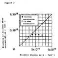
- Figure 3 is a diagram showing the relation between the electron concentration, the Si atom concentration and the silicon doping rate obtained in Example 1.
- Figure 4 is a sectional view of a hetero-junction crystal used in Example 1.
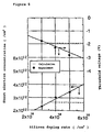
- Figure 5 is a diagram showing the relation between the the sheet carrier concentration, the sheet carrier concentration and the silicon doping rate for the hetero-junction crystal having the structure shown in Fig. 4 (where the solid lines represent calculated values, the dotted lines represent predicted values of Vt and Ns assuming an electron concentration saturation similar to that for the thick-film n-AlGaAs crystal, and the black circles represent experimental values).
- Figure 6 is a sectional view of a hetero-junction crystal used in Example 2.
- Figure 7 is a diagram showing the relation between the sheet electron concentration (Ns), the threshold voltage (Vt) and the silicon doping rate for a hetero-junction crystal having the structure of Fig. 6 (where the solid lines represent calculated values, the dotted lines represent calculated values of Vt and Ns assuming an electron concentration saturation similar to that for the thick-film n-AlGaAs crystal, and the black circles represent experimental values.)
- Figure 8 is a sectional view of the hetero-junction crystal used in Example 3.
- the concentration of the donor impurities that can actively exist in an n-type semiconductor has been considered to have an upper limit determined according to the value expressed by equation (1) associated with the particular substance.
- the present inventors have found that in an n-type semiconductor in contact with a substance having a different upper limit of donor concentration, the upper limit of donor impurities concentration of a semiconductor lower in the upper limit of donor impurities concentration can be increased by the action of a semiconductor with a higher upper limit of donor impurities concentration within the range in which electron transfer takes place through the junction (within the depletion layer).
- the present inventors have found that when semiconductors having different Fermi levels are brought into contact with each other, the Fermi level is locally reduced in the semiconductor layer depleted by electron tarnsfer and the self-compensation is not caused by the generation of a defect due to the Fermi level saturation mechanism, so that the donor impurities are effectively activated.
- the method of fabricating a semiconductor having an n-type semiconductor layer 1 with donor impurities added thereto as shown in Fig. 1 according to the present invention is characterized in that a semiconductor layer 2 having an energy value from vacuum level to Fermi level larger than the energy value from vacuum level to the lower end of the conduction band of the n-type semiconductor 1 with the donor impurities added thereto is junctioned with the n-type semiconductor 1, and donor impurities are doped in the range of thickness of the depletion layer generated in the n-type semiconductor layer 1 in contact with the junction boundary.
- This fabrication method can realize that the donor impurities concentration (N d ) in the range of thickness of the depletion layer generated in the n-type semiconductor layer 1 in contact with the junction boundary is at least 2.7 x 10 3 exp ⁇ -5.5(E C - E FS ) ⁇ x N C (where each symbol is defined the same as mentioned above).
- the thickness of the depletion layer of the n-type semiconductor layer is defined by a value obtained by dividing the total amount of electrons that have transfered from the n-type semiconductor layer 1 to the semiconductor layer 2 by the concentration of impurities doped into the n-type semiconductor layer 1.
- This value is theoretically equivalent to the thickness of a portion in the semiconductor layer 1 in the neighborhood of the junction boundary with the semiconductor layer 2 where the electron density per unit of volume is preferably 10 12 /cm 3 or less, or more preferably 10 15 /cm 3 or less, or most preferably 10 17 /cm 3 or less in the electron density distribution obtained by solving Poisson's equation and the Schrodinger's wave equation self-consistently taking into consideration the conduction band structure, the layer thickness and the impurities distribution in the semiconductor layers 1 and 2.
- the method of fabricating a semiconductor according to the present invention is preferably such that in the method described above, the energy value from vacuum level to Fermi level is replaced by the energy value from vacuum level to the lower end of the conduction band.
- This fabrication method can realize that the donor impurities concentration (N d ) in the range of thickness of the depletion layer generated in the n-type semiconductor layer 1 in contact with the junction boundary is at least 2.7 x 10 3 exp ⁇ -5.5(E C - E FS ) ⁇ x N C (where each symbol is defined the same as mentioned above).
- the ambient temperature for doping the impurities is preferably 550°C or higher.
- the semiconductor comprising the n-type semiconductor 1 according to the present invention may include a compound semiconductor or an element semiconductor.
- the compound semiconductor may include a 3-5 group compound semiconductor or a 2-5 group compound semiconductor
- the element semiconductor may include a 4-group semiconductor or a mixed-crystal conductor thereof.
- the 4-group semiconductors specifically include diamond, Si and Ge.
- Al x Ga (1-x) As (0 ⁇ x ⁇ 1), In y Al z Ga (1-y-x )As (0 ⁇ y ⁇ 1, 0 ⁇ z ⁇ 1) or the like can be used as the semiconductor layer 1 according to the present invention.
- y Ga (1-y )As (0 ⁇ y ⁇ 1) or the like can be used as the semiconductor layer 2 or the semiconductor layer 2' according to the invention.
- the concentration of donor impurities in the n-type semiconductor layer is at least 2.7 x 10 3 exp ⁇ -5.5(E C - E FS ) ⁇ x N C .
- the concentration of at least 3.9 x 10 3 exp ⁇ -5.5(E C - E FS ) ⁇ x N C is preferable. More preferably, the concentration is 5.0 x 10 3 exp ⁇ -5.5(E C - E FS ) ⁇ x N C , and a most preferable concentration is 6.0 x 10 3 exp ⁇ -5.5(E C - E FS ) ⁇ x N C or more.
- a measure of the upper limit of electron density in the semiconductor layer 1 is provided by the maximum impurities concentration defined by equation (1) for the semiconductor layer 2 junctioned with the semiconductor layer 1.
- an upper limit of course is provided also by the metallurgical solution limit of the donor elements in the n-type semiconductor.
- the thickness of the n-type semiconductor layer permitting the doping beyond the concentration limit indicated by equation (1) is within the range of thickness of the depletion layer generated in the portion in contact with the boundary.
- the effective donor concentration is saturated at an upper limit similar to that for a single unit, and addition of a dopant of an amount equal to or more than the saturation value increases the inherent defects requiring compensation. This inherent defect adversely affects the quality of the semiconductor, and therefore the concentration of added impurities in the regions other than the depletion layer is preferably held at or less than the value given by equation (1).
- the gist of the present invention lies in that in doping a high-concentration n-type semiconductor, a semiconductor low in Fermi level is brought into contact with the n-type semiconductor, so that the Fermi level of the n-type semiconductor layer is locally reduced within the range of the boundary depletion layer thereby to suppress the generation of defects to be compensated.
- a high-concentration doping which would be impossible with the single-layer semiconductor is realized.
- the semiconductor layer brought into contact with the n-type semiconductor for realizing the desired high-concentration doping may be a semiconductor layer having a lower Fermi level lower than the high-concentration doped layer.
- Such a semiconductor layer may include the above-mentioned hetero-junction, a semiconductor layer with a low electron concentration, a semiconductor layer having a large amount of impurities or defects with an electron capture level deep in the forbidden gap, a surface of semiconductor layer having a surface level, or a p-type semiconductor layer.
- the n-type semiconductor layer has been referred to in all of the above descriptions. Also, for the p-type semiconductor, unlike in the case of the n-type semiconductor, a high-concentration doping is locally realizable equal to or higher than the upper doping limit given by equation (2) within the range of the depletion layer generated in the neighborhood of the surface or the junction plane by bringing the p-type semiconductor into contact with a system higher in Fermi level.
- a method of fabricating a semiconductor comprising a p-type semiconductor layer 3 with acceptor impurities added thereto as shown in Fig. 2, characterized in that a semiconductor layer 4 having an energy value from vacuum level to Fermi level smaller than the energy value from vacuum level to the upper end of the valence band of the p-type semiconductor layer 3 with the acceptor impurities added thereto is junctioned with the p-type semiconductor layer 3, and acceptor impurities are doped within the range of the thickness of the depletion layer generated in the p-type semiconductor layer 3 in contact with the junction boundary.
- the thickness of the depletion layer in the p-type semiconductor layer is defined as a value obtained by dividing the total amount of the holes that have transfered from the p-type semiconductor layer 3 to the semiconductor layer 4 by the concentration of the impurities doped into the p-type semiconductor layer 3.
- This value is theoretically equivalent to the thickness of a portion in the semiconductor layer 3 in the neighborhood of the junction boundary with the semiconductor layer 4, where the hole density per unit of volume is preferably 10 12 /cm 3 or less, more preferably 10 15 /cm 3 , or most preferably 10 17 /cm 3 or less, in the hole density distribution obtained by solving Poisson's equation and Schrodinger's wave equation self-consistently taking into consideration the valence band structure, the layer thickness and the impurities distribution of the semiconductor layers 3 and 4.
- a method of fabricating a semiconductor in which the energy value from vacuum level to Fermi level in the above-mentioned method is replaced by the energy value from vacuum level to the upper end of the valence band.
- This fabrication method can realize the concentration (N a ) of acceptor impurities of at least 4.0 x 10 3 exp ⁇ -6.1(E FS - E V ) ⁇ x N V (where each symbol is defined the same as mentioned above) within the range of thickness of the depletion layer generated in the p-type semiconductor layer 3 in contact with the junction boundary.
- the ambient temperature for doping the impurities is preferably 550°C or higher.
- a semiconductor comprising a p-type semiconductor layer according to the invention may include a semiconductor illustrated above with reference to a semiconductor having the n-type semiconductor layer 1.
- Al x Ga (1-x) As (0 ⁇ x ⁇ 1), In y Al z Ga (1-y-z) As(0 ⁇ y ⁇ 1, 0 ⁇ z ⁇ 1) or the like can be used as the semiconductor layer 3 according to the invention, and In y Ga (1-y) As (0 ⁇ y ⁇ 1) or the like can be used as the semiconductor layer 4 according to the invention.
- a plurality of dopants having different solution limits or different connection sites can be used at a time with equal effect.
- an n-type AlGaAs crystal was prepared in the manner described below by the metal organic CVD (MOCVD) with a semi-insulating GaAs single crystal as a substrate.
- MOCVD metal organic CVD
- a substrate made of a GaAs single crystal having a clean surface which has a plane inclined by 0.4° in the direction of ⁇ 0-11 ⁇ from (100) plane is thermally cleaned in a mixed gas ambience of hydrogen gas and arsine in an epitaxial growth furnace.
- the arsine concentration in the ambience was adjusted to 0.83 mol% at 650° , and 2.95 x 10 -3 mol% of trimethyl gallium was added to the ambience thereby to epitaxially grow a GaAs layer 50 nm thick. Further, 7.38 x 10 -4 mol% of trimethyl aluminum was added to epitaxially grow an Al 0.2 Ga 0.8 As layer in the thickness of 300 nm.
- an n-type Al 0.2 Ga 0.8 As layer 500 nm thick with 5.80 x 10 -7 mol% to 4.09 x 10 -5 mol% of disilane added thereto was epitaxially grown, after which a semiconductor crystal was retrieved from a cooled growth furnace.
- the flow rate of the hydrogen gas used as a carrier gas was 45 SLM, and the epitaxial growth rate of the Al 0.2 Ga 0.8 As layer was about 20 nm/min.
- 1 SLM (1 standard litter per minute) is defined as a gas flow rate of one litter per minute under the standard condition (0°C and one atmosphere).
- the crystal thus retrieved was cleaved into about a 5-mm square of rectangle. Indium dots were attached to the four corners of this rectangle, which was then annealed for five minutes at 350°C in the hydrogen environment thereby to form an ohmic electrode. Then, electron concentration were measured by the Hall measurement(Van Der Pauw method) and thus the electron concentration was determined.
- the abscissa represents the silicon doping rate which is represented by the disilane flow rate specified with the doping rate set to 2 x 10 18 /cm 3 for the electron concentration of 2 x 10 18 /cm 3 .
- the doping rate and the electron concentration are proportional to each other.
- the Si concentration based on SIMS continues to increase in proportion to the doping rate.
- the electron concentration is saturated and has been found unable to increase beyond about 3 x 10 18 /cm 3 .
- the maximum electron concentration predicted from equation (1) is 3.5 x 10 18 /cm 3 , which substantially coincides with the saturation value obtained experimentally.
- a hetero-junction crystal composed of a 3-5 group compound semiconductor having the structure shown in Fig. 4 was prepared.
- the procedure and conditions for crystal growth are similar to those for the n-type Al 0.2 Ga 0.8 As layer in Comparative Example 1 except for the fact that trimethyl indium was added as a raw material for epitaxial growth of the In 0.2 Ga 0.8 As layer and the growth temperature of In 0.2 Ga 0.8 As layer was set to 600°C.
- the silicon doping rate in the n-type Al 0.2 Ga 0.8 As layer shown in Fig. 4 was changed in the range of 3 to 6 x 10 18 /cm 3 under the same condition as in Comparative Example 1.
- the crystal thus obtained was subjected to Hall measurement in a manner similar to the n-type Al 0.2 Ga 0.8 As layer described above thereby to determine the sheet electron concentration. Also, a specimen was prepared for measuring the capacitance-voltage characteristic in the manner described below.
- a portion of the epitaxial crystal specimen was cleaved by about 1/4 and retrieved, and the entire surface thereof was vapor-deposited with about 200 nm of aluminum metal. Then, the aluminum metal was separated into a circular portion 800 ⁇ m in diameter and the remaining portion 50 ⁇ m apart from the circular portion by photolithography.
- a pseudo-Schottky diode was prepared with a Schottky electrode formed of the circular portion and the opposite electrode of the remaining portion.
- an electron concentration profile was determined by the capacitance-voltage method with a negative voltage applied to the Schottky electrode.
- the voltage value with the electron concentration reduced to 1 x 10 15 /cm 3 was determined as a threshold voltage (Vt).
- the theoretical electrical characteristic of the epitaxial crystal prepared in the above-mentioned manner was determined in the following way. Specifically, on the basis of the structure obtained, the electron distribution of the structure was determined by solving Shroedinger's wave equation and Poisson's equation self-consistently. In the process, the GaAs surface level was assumed to be 0.9 eV from the lower end of the conduction band.
- the sheet electron concentration Ns obtained by Hall measurement and the value Vt obtained by the capacitance-voltage method are shown in Fig. 5 (closed circles).
- the conditions for crystal growth of the n-Al 0.2 Ga 0.8 As crystal layer and the disilane doping rate are the same as those used for the thick film evaluation in Comparative Example 1.
- the Ns value and the Vt value experimentally obtained should be constant as shown by dotted lines in the drawing. Actually, however, the experimental value was found to be proportional to the doping rate and substantially coincide with the calculated value.
- a hetero-structured crystal composed of a 3-5 group compound semiconductor having the structure shown in Fig. 6 was prepared.
- the procedure and conditions for crystal growth are similar to those for Example 1.
- the crystal thus obtained was subjected to the Hall measurement in a manner similar to Example 1 to determine the sheet electron concentration (Ns).
- the threshold voltage (Vt) was determined by the capacitance-voltage method.
- the sheet electron concentration Ns obtained by the Hall measurement and the value Vt obtained by the capacitance-voltage method are shown in Fig. 7 (black circles). Also, the Ns value and the Vt value obtained by calculations are shown by solid lines.
- the conditions for doping silicon in the n-type Al 0.2 Ga 0.8 As are identical to those used for thick film evaluation in the comparative example. Assuming that the silicon doping concentration in the n-type Al 0.2 Ga 0.8 As is saturated at about 3 x 10 18 /cm 3 or thereabout as indicated by the result obtained with the thick film in the comparative example, the Ns value and the Vt value experimentally obtained should assume a constant value as indicated by dotted lines in Fig. 6. Actually, however, the experimental value has been found to increase substantially at the same rate as the calculated value with the increase in the doping rate.
- a hetero-structured crystal composed of a 3-5 group compound semiconductor having a structure shown in Fig. 8 was prepared.
- the procedure and conditions for crystal growth are similar to those for Examples 1 and 2.
- the crystal layer structure is composed of GaAs and In 0.2 Ga 0.8 As.
- the silicon doping concentration of the substrate-side GaAs layer was maintained constant at 3 x 10 18 /cm 3 , and the 12-nm thick In 0.2 Ga 0.8 As layer was not doped or doped with silicon at the rate of 3 x 10 19 /cm 3 or at the rate of 6 x 10 19 /cm 3 .
- the 10-nm thick n-type GaAs layer formed on this assembly was doped with silicon at the rate of 3 x 10 19 /cm 3 or at the rate of 6 x 10 19 /cm 3 .
- metal electrodes were mounted on the crystal thus prepared and the contact resistance was measured. Minutely, rectangular metal electrodes of 150 ⁇ m x 100 ⁇ m in size were formed by photolithography and vacuum evaporation of the metal on the surface of a specimen crystal at spatial inter-electrode intervals of 5, 10, 15, 20, 25 and 30 ⁇ m. From the current-voltage measurements obtained with a 1-mA current supplied between the electrodes, the contact resistance value was determined by the TLM (transmission line method). The area up to the semi-insulative substrate portion other than the electrodes and those portions with the specified range of inter-electrode distance of 5 to 30 ⁇ m was removed by mesa etching. Three types of metal electrodes including Al (400 nm), Ti (50 nm)/Au (300 nm) and AuGe (600 nm)/Ni (200 nm)/Au (300 nm) were employed.
- an n-GaAs crystal 500 nm thick doped with silicon at the rate of 5 x 10 18 /cm 3 was prepared as a reference specimen, so that metal electrodes were formed and the contact resistance measured in similar fashion. The measurement was conducted either immediately after forming the electrodes or after annealing for 90 seconds in a 380°C hydrogen environment.
- An annealed AuGe/Ni/Au electrode is widely used as an ohmic electrode for n-GaAs.
- the silicon doping concentration is generally known to saturate at about 5 to 6 x 10 19 /cm 3 .
- the boundary of the semiconductor electrodes has such a high resistance as to be not conductive or has a high contact resistance.
- a satisfactory contact resistance of 3.8 x 10⁻⁵ ⁇ cm 2 could be obtained for the AuGe/Ni/Au electrode by annealing.
- the GaAs is known to have a high-density surface states.
- a Schottky barrier is generally known to develop due to the depletion layer formed in the semiconductor by the effect of surface states regardless of the type of the metal used as an electrode.
- a thin boundary depletion layer is formed with high-concentration doping.
- the current flow is facilitated due to the tunnel effect, thereby effectively forming an ohmic contact.
- an ohmic contact can be produced in GaAs by doping at the rate of 2 x 10 19 /cm 3 or more.
- the Ge diffusion occurring in the annealing process is considered to cause the high-concentration doping in the neighborhood of the boundary thereby to form an ohmic contact.
- a high-concentration impurities doping with a concentration equal to or more than the conventionally-known concentration value is possible, thereby making applications possible to high-performance hetero-junction devices having a high-concentration doped layer, an ohmic contact layer, devices utilizing the tunnel junction and other various semiconductor devices of which the development has thus far been hampered by the difficulty of high-concentration doping.
- the industrial significance of the invention therefore, is very high.
Landscapes
- Recrystallisation Techniques (AREA)
- Physical Deposition Of Substances That Are Components Of Semiconductor Devices (AREA)
- Crystals, And After-Treatments Of Crystals (AREA)
- Junction Field-Effect Transistors (AREA)
- Photovoltaic Devices (AREA)
Applications Claiming Priority (2)
| Application Number | Priority Date | Filing Date | Title |
|---|---|---|---|
| JP4372596 | 1996-02-29 | ||
| JP43725/96 | 1996-02-29 |
Publications (2)
| Publication Number | Publication Date |
|---|---|
| EP0793264A2 true EP0793264A2 (de) | 1997-09-03 |
| EP0793264A3 EP0793264A3 (de) | 1997-11-26 |
Family
ID=12671774
Family Applications (1)
| Application Number | Title | Priority Date | Filing Date |
|---|---|---|---|
| EP97103271A Ceased EP0793264A3 (de) | 1996-02-29 | 1997-02-27 | Dotierter Halbleiter mit hoher Konzentration |
Country Status (4)
| Country | Link |
|---|---|
| US (1) | US5982024A (de) |
| EP (1) | EP0793264A3 (de) |
| KR (1) | KR100519896B1 (de) |
| TW (1) | TW334592B (de) |
Families Citing this family (4)
| Publication number | Priority date | Publication date | Assignee | Title |
|---|---|---|---|---|
| JP3866149B2 (ja) * | 2002-05-08 | 2007-01-10 | 富士通株式会社 | 半導体装置の製造方法 |
| US8030188B2 (en) * | 2008-12-05 | 2011-10-04 | Electronics And Telecommunications Research Institute | Methods of forming a compound semiconductor device including a diffusion region |
| WO2010116701A1 (ja) * | 2009-04-07 | 2010-10-14 | 住友化学株式会社 | 半導体基板の製造方法および半導体基板 |
| WO2010116700A1 (ja) | 2009-04-07 | 2010-10-14 | 住友化学株式会社 | 半導体基板、半導体基板の製造方法、および電子デバイス |
Citations (1)
| Publication number | Priority date | Publication date | Assignee | Title |
|---|---|---|---|---|
| EP0696053A1 (de) * | 1994-06-29 | 1996-02-07 | Laboratoires D'electronique Philips | Verfahren zur Herstellung eines Feldeffekttransistors mit vertieftem Kanal |
Family Cites Families (4)
| Publication number | Priority date | Publication date | Assignee | Title |
|---|---|---|---|---|
| JPS56124273A (en) * | 1980-03-04 | 1981-09-29 | Semiconductor Res Found | Semiconductor device |
| US4686550A (en) * | 1984-12-04 | 1987-08-11 | American Telephone And Telegraph Company, At&T Bell Laboratories | Heterojunction semiconductor devices having a doping interface dipole |
| EP0430595B1 (de) * | 1989-11-27 | 1997-04-02 | Kabushiki Kaisha Toshiba | Verbindungshalbleiteranordnung |
| US5266818A (en) * | 1989-11-27 | 1993-11-30 | Kabushiki Kaisha Toshiba | Compound semiconductor device having an emitter contact structure including an Inx Ga1 -x As graded-composition layer |
-
1997
- 1997-02-24 KR KR1019970005598A patent/KR100519896B1/ko not_active Expired - Fee Related
- 1997-02-27 EP EP97103271A patent/EP0793264A3/de not_active Ceased
- 1997-02-27 US US08/807,394 patent/US5982024A/en not_active Expired - Lifetime
- 1997-03-03 TW TW086102506A patent/TW334592B/zh not_active IP Right Cessation
Patent Citations (1)
| Publication number | Priority date | Publication date | Assignee | Title |
|---|---|---|---|---|
| EP0696053A1 (de) * | 1994-06-29 | 1996-02-07 | Laboratoires D'electronique Philips | Verfahren zur Herstellung eines Feldeffekttransistors mit vertieftem Kanal |
Also Published As
| Publication number | Publication date |
|---|---|
| KR970063777A (ko) | 1997-09-12 |
| TW334592B (en) | 1998-06-21 |
| EP0793264A3 (de) | 1997-11-26 |
| KR100519896B1 (ko) | 2006-04-28 |
| US5982024A (en) | 1999-11-09 |
Similar Documents
| Publication | Publication Date | Title |
|---|---|---|
| EP0457508B1 (de) | Diamant-Halbleiteranordnung | |
| US8610450B2 (en) | Method of measuring electrical characteristics of semiconductor wafer | |
| Martin et al. | Electrical properties of GaAs/GaN/GaAs semiconductor-insulator-semiconductor structures | |
| US8872231B2 (en) | Semiconductor wafer, method of producing semiconductor wafer, and electronic device | |
| US5952672A (en) | Semiconductor device and method for fabricating the same | |
| US6841435B2 (en) | Method for fabricating a GaInP epitaxial stacking structure | |
| US6982441B2 (en) | Semiconductor device with a super lattice buffer | |
| EP0045181A2 (de) | Halbleiterbauelement mit Heteroübergang und hoher Elektronenbeweglichkeit und Herstellungsverfahren | |
| US5982024A (en) | High concentration doped semiconductor | |
| US4297783A (en) | Method of fabricating GaAs devices utilizing a semi-insulating layer of AlGaAs in combination with an overlying masking layer | |
| US5024967A (en) | Doping procedures for semiconductor devices | |
| US6225200B1 (en) | Rare-earth element-doped III-V compound semiconductor schottky diodes and device formed thereby | |
| Rosztoczy et al. | Growth and evaluation of epitaxial GaAs for microwave devices | |
| Andre et al. | Growth of (Al, Ga) AsGaAs heterostructures for HEMT devices | |
| KR100944883B1 (ko) | Pn 접합을 갖는 박막 결정 웨이퍼 및 그 제조 공정 | |
| Houng | CBE growth of AlGaAs/GaAs heterostructures and their device applications | |
| US5426068A (en) | Method of manufacturing compound semiconductor wafer | |
| Eda et al. | photoluminescence in AlGaAs/GaAs heterojunction bipolar transistors | |
| JPH09293854A (ja) | 高濃度ドープ半導体およびその製造方法 | |
| Wang et al. | Structural and electrical properties of GaSb, AlGaSb and their heterostructures grown on GaAs by metalorganic chemical vapor deposition | |
| JPH0289325A (ja) | 化合物半導体の構造体及びその形成方法 | |
| Shao et al. | Low resistance ohmic contacts to p-Ge/sub 1-x/C x on Si | |
| Sandhu et al. | p+/N GaAs-AlGaAs heterostructures grown by gas source MBE using gaseous p-and n-type dopant sources | |
| Chen et al. | Electrical properties of Si1− x− yGexCy and Ge1− yCy alloys | |
| Rigo et al. | InP: Fe semi-insulating layers by chemical beam epitaxy |
Legal Events
| Date | Code | Title | Description |
|---|---|---|---|
| PUAI | Public reference made under article 153(3) epc to a published international application that has entered the european phase |
Free format text: ORIGINAL CODE: 0009012 |
|
| AK | Designated contracting states |
Kind code of ref document: A2 Designated state(s): DE FR GB |
|
| PUAL | Search report despatched |
Free format text: ORIGINAL CODE: 0009013 |
|
| AK | Designated contracting states |
Kind code of ref document: A3 Designated state(s): DE FR GB |
|
| 17P | Request for examination filed |
Effective date: 19980518 |
|
| 17Q | First examination report despatched |
Effective date: 20041018 |
|
| RAP1 | Party data changed (applicant data changed or rights of an application transferred) |
Owner name: SUMITOMO CHEMICAL COMPANY, LIMITED |
|
| 17Q | First examination report despatched |
Effective date: 20041018 |
|
| STAA | Information on the status of an ep patent application or granted ep patent |
Free format text: STATUS: THE APPLICATION HAS BEEN REFUSED |
|
| 18R | Application refused |
Effective date: 20110217 |