EP0796521B1 - Vorrichtung zur störsicheren modulation und demodulation von analogen signalen zur nachrichtenübertragung über die schirmungen von energieübertragungskabeln - Google Patents
Vorrichtung zur störsicheren modulation und demodulation von analogen signalen zur nachrichtenübertragung über die schirmungen von energieübertragungskabeln Download PDFInfo
- Publication number
- EP0796521B1 EP0796521B1 EP95941652A EP95941652A EP0796521B1 EP 0796521 B1 EP0796521 B1 EP 0796521B1 EP 95941652 A EP95941652 A EP 95941652A EP 95941652 A EP95941652 A EP 95941652A EP 0796521 B1 EP0796521 B1 EP 0796521B1
- Authority
- EP
- European Patent Office
- Prior art keywords
- digital
- frequency
- clock signal
- bandpass filter
- clocked
- Prior art date
- Legal status (The legal status is an assumption and is not a legal conclusion. Google has not performed a legal analysis and makes no representation as to the accuracy of the status listed.)
- Expired - Lifetime
Links
Images


Classifications
-
- H—ELECTRICITY
- H03—ELECTRONIC CIRCUITRY
- H03C—MODULATION
- H03C3/00—Angle modulation
-
- H—ELECTRICITY
- H02—GENERATION; CONVERSION OR DISTRIBUTION OF ELECTRIC POWER
- H02J—ELECTRIC POWER NETWORKS; CIRCUIT ARRANGEMENTS OR SYSTEMS FOR SUPPLYING OR DISTRIBUTING ELECTRIC POWER; SYSTEMS FOR STORING ELECTRIC ENERGY
- H02J13/00—Circuit arrangements for providing remote monitoring or remote control of equipment in a power distribution network
- H02J13/13—Circuit arrangements for providing remote monitoring or remote control of equipment in a power distribution network characterised by the transmission of data to equipment in the power network
- H02J13/1311—Circuit arrangements for providing remote monitoring or remote control of equipment in a power distribution network characterised by the transmission of data to equipment in the power network using the power network as support for the transmission
- H02J13/1313—Circuit arrangements for providing remote monitoring or remote control of equipment in a power distribution network characterised by the transmission of data to equipment in the power network using the power network as support for the transmission using pulsed signals
-
- Y—GENERAL TAGGING OF NEW TECHNOLOGICAL DEVELOPMENTS; GENERAL TAGGING OF CROSS-SECTIONAL TECHNOLOGIES SPANNING OVER SEVERAL SECTIONS OF THE IPC; TECHNICAL SUBJECTS COVERED BY FORMER USPC CROSS-REFERENCE ART COLLECTIONS [XRACs] AND DIGESTS
- Y02—TECHNOLOGIES OR APPLICATIONS FOR MITIGATION OR ADAPTATION AGAINST CLIMATE CHANGE
- Y02E—REDUCTION OF GREENHOUSE GAS [GHG] EMISSIONS, RELATED TO ENERGY GENERATION, TRANSMISSION OR DISTRIBUTION
- Y02E60/00—Enabling technologies; Technologies with a potential or indirect contribution to GHG emissions mitigation
-
- Y—GENERAL TAGGING OF NEW TECHNOLOGICAL DEVELOPMENTS; GENERAL TAGGING OF CROSS-SECTIONAL TECHNOLOGIES SPANNING OVER SEVERAL SECTIONS OF THE IPC; TECHNICAL SUBJECTS COVERED BY FORMER USPC CROSS-REFERENCE ART COLLECTIONS [XRACs] AND DIGESTS
- Y04—INFORMATION OR COMMUNICATION TECHNOLOGIES HAVING AN IMPACT ON OTHER TECHNOLOGY AREAS
- Y04S—SYSTEMS INTEGRATING TECHNOLOGIES RELATED TO POWER NETWORK OPERATION, COMMUNICATION OR INFORMATION TECHNOLOGIES FOR IMPROVING THE ELECTRICAL POWER GENERATION, TRANSMISSION, DISTRIBUTION, MANAGEMENT OR USAGE, i.e. SMART GRIDS
- Y04S40/00—Systems for electrical power generation, transmission, distribution or end-user application management characterised by the use of communication or information technologies, or communication or information technology specific aspects supporting them
- Y04S40/12—Systems for electrical power generation, transmission, distribution or end-user application management characterised by the use of communication or information technologies, or communication or information technology specific aspects supporting them characterised by data transport means between the monitoring, controlling or managing units and monitored, controlled or operated electrical equipment
- Y04S40/121—Systems for electrical power generation, transmission, distribution or end-user application management characterised by the use of communication or information technologies, or communication or information technology specific aspects supporting them characterised by data transport means between the monitoring, controlling or managing units and monitored, controlled or operated electrical equipment using the power network as support for the transmission
Definitions
- the invention relates to a circuit which interfaces between the shields serving as transmission links of power transmission cables and the facilities for Specification and processing of the respective messages in the Rule digital computer, for feeding or receiving the present in the form of analog, frequency-modulated signals News is needed.
- On the sending side of the Circuit serves to generate the signals from current digital default values, i.e. for so-called modulation.
- On the reception side of the circuit is used for recovery the digital default values from received analog signals, i.e. for so-called demodulation.
- Such a circuit is often referred to as a modem or a modem circuit.
- sinusoidal, analog signals with two different transmission frequencies formed which is called the upper and lower frequency can be.
- the high-frequency switching cycle between the transmission frequencies i.e. which is a frequency modulation representing key shift, is from the current bit pattern of the depending on the respective digital default value. It is the a transmission frequency is unique for each of the two binary values assigned.
- demodulating in the receiving section of a Modems are recognized, which of the two transmission frequencies is currently active Will be received. This then becomes the corresponding binary Assigned value. From the sequence of the resulting in this way binary values will eventually become the particular message representative digital default value reconstructed.
- the circuit according to the invention is used specifically in the so-called cable shield communication.
- the messages in the form of analog, frequency-modulated Signals via the shields, in particular for energy distribution serving high-voltage cables.
- Both Messages are usually control and status signals.
- Control signals are usually from one Central computers generate and serve to control network resources in the energy distribution network, e.g. of step transformers, Circuit breakers and the like.
- such messages can also signal status signals with what the current operating state of the energy distribution network through the network resources distributed therein be communicated to the central computer.
- the messages can be sent to the relay station being received be directed.
- the digitally reconstructed from this Default values can then e.g. point out as control signals which is the network resource located in the respective network point affect.
- control signals which from the central computer to an in network equipment located at another network point are, e.g. status signals, which of one located in a certain other network point Network resources are directed to the central computer.
- the analog, frequency modulated signals from each relay station from the direction of a power transmission cable received and demodulated. Only now is a detection of that to another relay station or addressing directed to the central computer in the local Digital computer of the respective modem possible.
- the cable screen network used for transmission therefore has one very special topology. This is particularly marked through those with relay stations and one integrated each Modem circuit occupied interfaces of the cable shields in the nodes of the energy transmission network. These represent breakpoints in the chain of cable shields existing transmission path. From this is why there are particularly high demands on quality the transmission of messages.
- the modulation and demodulation in the modem of each relay station must therefore be special be robust, i.e. insensitive to the coupling of interference when transmitting into any cable shield or can occur at one of the many nodes.
- the invention is based, as simple as possible Specify modem circuit with which a message in and decoupling into and out of the shields of power transmission cables nevertheless possible with high interference immunity is.
- EP 0560071A is a device for interference-free modulation and Demodulation known that a digital modulator and demodulator and means for Has generation of a central precision clock. On the receiving side of this known device, however, there is no clocked one Bandpass filter and Schmidt trigger available.
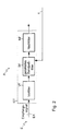
- Figure 1 shows the block diagram of the modem circuit according to the invention.
- a vertical one A-D dividing line and a horizontal dividing line E-S entered.
- the horizontal dividing line E-S the receiving section E and the transmitting section S of the modem circuit are delimited.
- S of the modem circuit additionally delimited one analog part A and one digital part D, i.e. each a part in which analog signal processing or digital Signal processing is carried out.
- the receiving part E of the circuit according to the invention analog, from another modem into the energy transmission network fed-in, frequency-shift-keyed signals as received signals EK from the shielding of the neighboring, local Power transmission cable removed and in Figure 1 on the fed left.
- These are in the analog part of the Receiving part E in a central precision cycle T timed bandpass filter GT processed and one Interface between analog and digital part of the Receiving part E forming Schmitt trigger ST supplied.
- This derives from the processed analog reception signals rectangular trigger signals TR, which a digital Demodulator DDM, also from the central precision clock T is operated as control signals are supplied.
- This demodulates the trigger signals TR by determining the current one Transmission frequency of the received signals, i.e.
- the resulting current demodulated Bits is in the form of a serial receive bit stream EBS fed to a local computer CPU at its data input. This finally decodes from the current one "Pattern" of the bitstream EBS the actual default values, i.e. the respective message content.
- the computer communicates CPU via an output data bus ADB usually with a Central computer KP. This organizes the message transmission and thus the control of an entire power transmission cable network.
- each one is in the power transmission cable network distributed relay stations a modem included according to the circuit of FIG. 1.
- the computer CPU communicates via the output data bus ADB with the control elements of the respective network equipment.
- the core of the modem circuit according to the invention is the control of the essential elements of the circuit both on the Receiving side E and on the transmitting side S via a central Precision control clock T as a common time base or reference.
- the modulation on the transmission side and the demodulation on the receiving side is a particularly precise modulation and demodulation of transmitted signals possible, i.e. a narrowband and thus interference-free transmission overall.
- the central precision control clock T can by a separate Precision clock PT are provided, as in the Example of Fig. 1 is shown. On the other hand, there is also the possibility that the precision clock in the computer CPU is generated with high precision.
- the central generation of a precision control clock according to the invention T for all essential elements of the modem circuit of Figure 1 has a number of advantages.
- the invention Design of the modem circuit thus comes Transmission quality of the entire message transmission over the Cable shields of the energy transmission cables are good. This causes in particular a lower sensitivity of the Circuit versus the coupling of disturbances, which are just when transmitting messages via the shields of energy transmission cables to a particularly strong extent may occur.
- the circuit concept according to the invention possible to realize a particularly narrow-band transmission.
- the circuit concept according to the invention is thus particularly suitable for the use of two narrow in value characteristic frequencies lying next to each other. Upper and lower frequency can only by an unusually small carrier frequency swing from e.g. about 0.5 kilo heart separated.
- the digital demodulator DDM and the digital Modulator DM via the central precision clock T can namely a particularly high frequency stability can be achieved. It is thus possible, even closely spaced top and To easily modulate underfrequencies on the transmission side and especially on the reception side simple and to demodulate again without interference.
- the suppression of interference which in the analog frequency modulated signals coupled onto the shields of the power transmission cables is particularly effective.
- the clocked bandpass filter GT in the analog part A of the receiving part E of the circuit according to the invention has at least the task of processing the analog received signals EK in such a way that contained disturbing high frequency components and disruptive low frequency components, which DC offset are similar, are filtered out.
- the frequency spectrum the filtered analog signals are thus cropped that only contain frequencies from one area are as close as possible to that between the modulation used values of upper and lower frequency.
- the center frequency of the clocked bandpass filter GT becomes According to the invention of the central precision clock PT Circuit derived. Because the center frequency is very precise and can be stably specified, the transmission can be advantageous be designed narrow-band.
- the filter center frequency then lies as precisely as possible in the middle of the upper and lower frequency, between those in modulation and demodulation is keyed. This increases the interference immunity of the data transmission significantly improved.
- the analogue processed by the clocked bandpass filter GT Receive signals EK are now a Schmitt trigger ST fed. This forms the interface between analog Part A and digital part D of the circuit according to the invention.
- the Schmitt trigger ST contains at least one comparator, with which the processed receive signals EK in at least one frequency-identical square wave signal TR are converted. This again serves to trigger the subsequent digital Demodulator DDM.
- the digital demodulator DDM's job is frequency of the analog received signals EK to be recorded and this possible clearly assign the upper and lower frequency value.
- the digital demodulator has at least one a reference counter to which the trigger signal TR from the Schmitt trigger ST is supplied. This counts the period of each vibration, i.e. the the distance of the trigger signals TR off, so that a frequency measurement results.
- the counting clock of the reference counter also becomes from the central precision clock T of the precision clock generator PT certainly.
- the precision cycle T is fulfilled again the function of a central time base for the entire modem circuit. This can be used for frequency detection set the necessary frequency marks precisely.
- the hub of the Carrier frequency can thus be small, so that this narrowband transmission reached a significant Improvement of the immunity to interference of the invention Modem circuit causes.
- Due to the digital version of the Demodulators DDM also have no tolerances, temperature drifts and age-related level shifts. The hardware expenditure is reduced by this design greatly reduced in demodulation accuracy.
- the digital one Demodulator can be used with simple digital components such as e.g. Realize gates, flip-flops, counters. In contrast in known demodulator circuits, e.g. at a Intermediate frequency demodulator, a quadrature decoder or one Phase locked loop demodulator significantly reduces the amount of hardware greater.
- the circuit according to the invention is specific to the Data transmission via the shields of high-voltage cables existing conditions optimally adapted.
- the above described modem circuit can despite reduced hardware expenditure a particularly high level of interference immunity during data transmission due to a narrow-band transmission spectrum reached.
- the clocked bandpass filter GT is advantageous in the form of a clocked capacitor filter realized.
- Such filters are also known as "Switched Capacitor Filters".
- Switchched Capacitor Filters At This clocked filter can help in determining the frequency characteristics to an external circuit with real Capacitors are dispensed with. These would have to be very precise be good temperature and aging behavior and would therefore be expensive.
- the location of the pole points of the filter is rather determined by the value of the central precision clock T and determined a simple, external resistor circuit. Despite the simple structure of such a filter this has a very high quality and reproducible filter properties.
- the clocked bandpass filter GT consists of a cascade of several sub-filters. For example, as a block of four universal switched capacitor sub-filters be constructed.
- the partial filters have good frequency selectivity can be achieved.
- a carrier frequency swing e.g. approximately
- the bandwidth of the clocked bandpass filter is 0.5 kilohertz preferably about 1.8 kHz.
- the clocked bandpass filter GT can advantageously be provided by an additional Pre-filter and, if necessary, an additional one Post-filters can be added.
- Such a filter chain GT is shown in the example of Figure 2 and insists on a Prefilter VF, the actual clocked bandpass filter BF and a post filter NF.
- Analog receive signals EK are advantageous in one the properties of a bandpass pre-filter VF subjected to a first processing.
- the Low pass characteristics of the pre-filter can disruptive frequency components to avoid looping them in right at the input of the modem circuit according to the invention be filtered out. This will reduce the sensitivity to interference the circuit improved.
- design and dimensioning the other elements in the receiving part of the circuit, in particular the clocked bandpass filter BF and the digital demodulator DDM considerably simplified.
- the high-pass characteristics of the pre-filter can be a so-called constant component, also called offset, in the lower Frequency range can be suppressed. This also creates design and dimensioning of the other circuit parts significantly simplified and in particular their mode of operation improved, because by avoiding a possible DC component maintain the input dynamics on subsequent filters can be.
- the pre-filter VF is advantageous in the form of an active, continuous Bandpass filter preferably carried out 1st order and e.g. with an operational amplifier and RC circuit realized.
- This can include advantageous as a so-called anti-aliasing filter for the following clocked bandpass filter Serve BF. Since the actual "filter work" from subsequent, clocked bandpass filter BF is performed, its filter center frequency via the central precision clock T exactly to the respective existing values of the upper and Underfrequency is tuned, the bandwidth or the Cutoff frequencies of the pre-filter VF are not exactly the same as for the Modulation and demodulation of existing frequency relationships be coordinated. Elaborate circuit measures for their Constant maintenance can thus advantageously be avoided. Even for the suppression of a DC component, there is only one approximate coordination is sufficient.
- the pre-filter VF advantageously also contains means for Gain adjustment. This allows the signal level of the received, analog input signals EK to the input voltage range the subsequent elements of the circuit, in particular of the bandpass filter. It will advantageous on the one hand for further signal processing required minimum value of the signal level ensured. On the other hand is avoided that by exceeding a maximum Signal level in the receiving part of the invention Modem circuit following elements are overridden.
- the Setting the gain in the pre-filter VF has the special advantage that no reinforcements in the further circuit need to be done more.
- the signal-to-noise ratio can hereby be considerable be improved.
- the analog input signals can be advantageous by an additional Postfilter NF following the clocked bandpass filter BF can be further processed.
- the clocked bandpass filter BF may be on as a switched capacitor filter whose output noise is attenuated, which also as a loop through or crosstalk of the bandpass clock referred to as.
- it can be used in the clocked Bandpass filter BF possibly occurring DC component can be suppressed so that the received signal is symmetrical
- the reference ground of the circuit remains. Noise-free and symmetrical Received signals favor their error-free conversion into square wave signals in the subsequent Schmitt trigger ST.
- the Postfilter NF can be advantageous as an active, continuous Bandpass filter preferred 1st order e.g. with an operational amplifier and RC wiring can be implemented. Due to the advantageous structure of the modem circuit according to the invention As with the pre-filter VF, there are none with the post-filter NF high demands on the adherence to exact values of bandwidth or corner frequencies.
- clocked bandpass filter BF and post-filter NF existing clocked bandpass filter GT prepares the analog Received signals EK such that disturbing high frequency components and low-frequency, DC-like Offset components are filtered out, and that the signals one to analog reference ground of the circuit symmetrical sinusoidal Have shape.
- the signal behavior of a preferred embodiment 3 is shown for a Schmitt trigger ST.
- This forms the interface between the analog and digital receiver E.
- a filtered via the clocked bandpass filter GT, sinusoidal and to the analog mass of the modem circuit symmetrical received signal EK is in the Schmitt trigger ST preferably by means of two comparators in two complementary, frequency-equivalent square wave signals / S and / R converted. This are a digitized image of the analog received signal EK.
- the square wave signals / S and / R represent this Execution of the output signal "TR" of the Schmitt trigger ST represents.
- the Schmitt trigger advantageously has additional means with which the comparators one above or below the reference mass the threshold voltage value of the modem circuit + Uh or -Uh can be specified.
- the Comparators not at the zero response of the sinusoidal receive signal Switch EK, but only when one is reached Threshold voltage + Uh or -Uh.
- the resulting Switching hysteresis causes one of the so-called background noise Independent, flutter-free switching of the Schmitt trigger. This advantageously reduces noise causes.
- the amount of the threshold voltage Uh is preferably adjustable. This allows the sensitivity of the Schmitt trigger ST on the current noise ratios on the as Coordinate cable shields serving the transmission route.
- the comparators in the Schmitt trigger in each Switch period in the same place the Amount of threshold voltage does not depend on the frequency of the square wave signals / S, / R off. Their frequency is preserved and thus their function as frequency-identical trigger signals for the digital demodulator DDM.
- the signal behavior at the input of a preferred embodiment of the digital demodulator DDM is an example of Fig.4 shown.
- the digital demodulator DDM instructs its input preferably has an RS flip-flop whose level-sensitive Set and reset inputs the trigger signals / S and / R of the Schmitt trigger ST are supplied. This will the complementary flip-flop outputs Q and / Q are set.
- a flip-flop with level-active set and reset inputs advantageous a possibly still existing vibration in the / S and / R signals, denoted by bouncing in FIG. 4, are suppressed.
- the positive edges of the / Q signal differentiated and from it generates an internal trigger signal TS. Its frequency corresponds to the frequency of an analog reception signal EK.
- a sequence control in the digital demodulator DDM is included every positive edge of the internal TS trigger signal is triggered.
- the time between the positive trigger edges can be with a reference counter driven by central precision clock T. measured or the meter reading can by a digital Window comparator can be evaluated.
- the counter reading of the reference counter is preferred with compared three comparison values, which three frequency marks correspond.
- One of the three frequency marks serves as a so-called Center frequency between the upper and lower frequency. This makes it possible in the demodulator to recognize whether a received instantaneous frequency higher or lower than the center frequency is, and thus either the upper frequency or the Underfrequency is to be assigned. To limit this double Frequency windows serve an additional upper frequency limit and an additional underfrequency limit. Now it’s in Demodulator also possible to detect whether an outside of the permissible value range lying, impermissible frequency was received, i.e. whether the current instantaneous frequency is greater than the upper frequency limit or less than the lower frequency limit is.
- the modulator contains advantageous a digital frequency generator that between is keyed the two characteristic frequencies. Because of the invention Circuit concept is the digital frequency generator very precise in frequency, because the respective values of upper and lower frequency in the modulator according to the invention the central precision cycle T are instructed.
- the digital one Frequency generator probes approximately without delay between the two characteristic frequencies.
- the so-called digital modulator DM is preferred Continuous phase frequency shift keying modulation method applied. It is between the upper frequency FL and lower frequency FH switched. After activation of the digital modulator DM via a control signal SP is corresponding to that respective logic level of the digital modulator DM from Computer CPU serially supplied transmit bit stream SBS the upper or. Underfrequency generated. In the example in Fig. 5, this indicates Current bit of the send bit stream SBS after the modulator has been released to a high level. For this time it becomes an example an analog signal is sent, which is the underfrequency FL has. In the second half of the release period of the Modulators assigns the current bit of the transmit bit stream SBS low level. An analogue will then be used for this time Signal sent, which has the upper frequency FH.
- the keying between upper and lower frequency FL and FH is 5 also in the course of the transmission bit stream SBS by a falling edge marked.
- Frequency shift keying is advantageously carried out when a Zero crossing in the respectively active high-frequency or under-frequency transmission signal. This is done by using a so-called phase coherent continuous phase frequency shift Keying modulation in the digital modulator DM causes. This is represented in FIG. 5 by sampling with the signal MOD. By the suppression of the phase jumps achieved a slight shift key delay is caused, which is also entered in Fig. 5. For suppression a simple logic is sufficient for the phase jumps.
- the digital version of the modulator has the advantage that no switching between two separate, in terms of frequency different, non-synchronizable oscillators necessary is.
- Such an embodiment would have a variety of Have disadvantages. This would be the case with frequency shift keying inevitably larger phase jumps occur. To compensate for them the bandwidth to be transmitted would have to be increased, which in turn would affect immunity to interference. Since there are no two analog oscillators for generating the both characteristic frequencies are used, neither occur Settling times, which are in the range of milliseconds can lie. Such settling times would be separated by two Oscillators are needed because they are the switch between have to settle again each time. Rather, the inventive concept is based on a digital one Modulator, the one, from the central precision clock T driven digital frequency generator. This can almost instantaneous between upper and lower frequency can be switched.
- the low-pass filter TP preferably additionally contains a trapezoidal generator.
- the transmission signal in converted a symmetrical trapezoidal waveform.
- Fig.6 is the transmission signal of an advantageous embodiment of a such low-pass filter TP at the output of the transmitting part S the shown modem circuit according to the invention.
- the low pass filter also represents the interface between the digital Part D and the analog part A. This has the advantage that the further processing of the now quasi-analog Transmitting signals, in particular filtering them on the receiving side another modem circuit, considerably easier becomes.
- This trapezoid generator in the low-pass filter can only be used implement an operational amplifier.
- a subsequent one simple 2nd order low-pass filter is sufficient for the harmonic To suppress vibrations in the upper area again.
- This 2nd order low-pass filter can also be used implement an operational amplifier with RC circuit.
- This circuit concept can be used with only two operational amplifiers from a square wave signal a frequency modulated Low harmonics and therefore easy to transmit and generate demodulable sine signal.
- Channel 7 finally shows a two-channel embodiment of the invention Modem circuit.
- Channel 1 on the reception side E consists of a clocked bandpass filter GT1, a Schmitt trigger ST1 and a digital demodulator DDM1.
- the clocked bandpass filter GT1 is again advantageous from a chain, which is a pre-filter VF1, a clocked Contains bandpass filter BF1 and a post filter NF1.
- Channel 2 on the receiving side E is the same Way from a clocked bandpass filter GT2, a Schmitt trigger ST2 and a digital demodulator DDM2.
- the clocked Bandpass filter GT2 in turn advantageously consists of a Chain, which is a pre-filter VF2, a clocked bandpass filter BF2 and a post filter NF2 contains.
- a Chain which is a pre-filter VF2
- a clocked bandpass filter BF2 and a post filter NF2 contains.
Landscapes
- Engineering & Computer Science (AREA)
- Power Engineering (AREA)
- Digital Transmission Methods That Use Modulated Carrier Waves (AREA)
- Noise Elimination (AREA)
- Transmitters (AREA)
Description
- Fig. 1 :
- ein Blockschaltbild der erfindungsgemäßen Modemschaltung für die Nachrichteneinspeisung in bzw. Auskopplung aus den Schirmungen von Energieübertragungskabeln,
- Fig.2 :
- eine vorteilhafte Ausführung eines getakteten Bandpaßfilters in der erfindungsgemäßen Modemschaltung,
- Fig.3 :
- das Signalverhalten einer vorteilhaften Ausführungsform eines Schmitt-Triggers im Empfangsteil der erfindungsgemäßen Modemschaltung,
- Fig.4 :
- das Signalverhalten am Eingang einer vorteilhaften Ausführungsform eines digitalen Demodulators im Empfangsteil der erfindungsgemäßen Modemschaltung,
- Fig.5 :
- das Signalverhalten einer vorteilhaften Ausführungsform eines digitalen Modulators im Sendeteil der erfindungsgemäßen Modemschaltung,
- Fig.6 :
- das Signalverhalten einer vorteilhaften Ausführungsform eines Tiefpaßfilters am Ausgang des Sendeteiles der erfindungsgemäßen Modemschaltung, und
- Fig.7 :
- das Beispiel einer zweikanaligen Ausführung der erfindungsgemäßen Modemschaltung.
Claims (13)
- Vorrichtung zur störsicheren Modulation und Demodulation von analogen Signalen, welche frequenzmoduliert über die Schirmungen von Energieübertragungskabeln übertragen werden, wobeia) auf einer Empfangsseite (E) zumindest eine Reihenschaltung aus einem getakteten Bandpaßfilter (GT), einem Schmitt-Trigger (ST) und einem digitalen Demodulator (DDM), und auf einer Sendeseite (S) zumindest einen digitalen Modulator (DM) vorhanden ist, undb) Mittel (PT;CPU) zur Erzeugung eines zentralen Präzisionstaktes (T) vorhanden sind, welcher zumindest dem getakteten Bandpaßfilter (GT) und dem digitalen Demodulator (DDM) auf der Empfangsseite (E), und dem digitalen Modulator (DM) auf der Sendeseite (S) als eine gemeinsame Zeitbasis zugeführt wird.
- Vorrichtung nach Anspruch 1, wobei der digitale Modulator (DM) auf der Sendeseite (S) mindestens einen vom zentralen Präzisionstaktes (T) getriebenen digitalen Frequenzgenerator enthält, der die Kennfrequenzen (FL,FH) für die Frequenzmodulation zu sendender Vorgabewerte hochgenau aus dem Präzisionstakt (T) ableitet.
- Vorrichtung nach Anspruch 2, wobei zu sendende digitale Vorgabewerte im digitalen Modulator (DM) durch modulationsgesteuerte Umtastung des digitalen Frequenzgenerators zwischen einer Ober- und einer Unterfrequenz als Kennfrequenzen einer FSK-Modulation unterzogen werden.
- Vorrichtung nach Anspruch 2 oder 3, wobei der digitale Frequenzgenerator im digitalen Modulator (DM) phasenkohärent nur bei Auftreten eines Nulldurchganges bei einer der Kennfrequenzen zwischen Ober- und Unterfrequenz umtastet.
- Vorrichtung nach einem der vorangegangenen Ansprüche, wobei dem digitalen Modulator (DM) auf der Sendeseite (S) ein Tiefpaßfilter (TP) nachgeschaltet ist.
- Vorrichtung nach Anspruch 5, wobei das Tiefpaßfilter (TP) einen Trapezgenerator enthält.
- Vorrichtung nach einem der vorangegangenen Ansprüche, wobei das getaktete Bandpaßfilter (GT) als getaktetes Kondensatorfilter ausgeführt ist und die Mittenfrequenz des Bandpaßfilters (GT) vom zentralen Präzisionstakt (T) bestimmt wird.
- Vorrichtung nach einem der vorangegangenen Ansprüche, wobei dem getakteten Bandpaßfilter (GT) ein Vorfilter (VF) vorgeschaltet ist, welches als aktives kontinuierliches Bandpaßfilter bevorzugt 1. Ordnung ausgeführt ist.
- Vorrichtung nach Anspruch 8, wobei das Vorfilter (VF) Mittel zur Einstellung der Verstärkung der Signalpegel aufweist.
- Vorrichtung nach einem der vorangegangenen Ansprüche, wobei dem getakteten Bandpaßfilter (GT) ein Nachfilter (VF) nachgeschaltet ist, welches als aktives kontinuierliches Bandpaßfilter bevorzugt 1. Ordnung ausgeführt ist.
- Vorrichtung nach einem der vorangegangenen Ansprüche, wobei der digitale Demodulator (DDM) einen Referenzzähler zur Auszählung der Periodendauern analoger Empfangssignale (EK) enthält, dessen Zähltakt vom zentralen Präzisionstakt (T) bestimmt wird.
- Vorrichtung nach Anspruch 11, wobei am Eingang des digitalen Demodulators (DDM) ein Flip-Flop mit pegelsensitiven Set- und Reset-Eingängen vorhanden ist.
- Vorrichtung nach einem der vorangegangenen Ansprüche, wobei der Schmitt-Trigger (ST) für die Erzeugung einer Schalthysterese Mittel zur Vorgabe einer Schwellspannung (± Uh) aufweist.
Priority Applications (1)
| Application Number | Priority Date | Filing Date | Title |
|---|---|---|---|
| EP95941652A EP0796521B1 (de) | 1994-12-08 | 1995-12-01 | Vorrichtung zur störsicheren modulation und demodulation von analogen signalen zur nachrichtenübertragung über die schirmungen von energieübertragungskabeln |
Applications Claiming Priority (4)
| Application Number | Priority Date | Filing Date | Title |
|---|---|---|---|
| EP94119418 | 1994-12-08 | ||
| EP94119418 | 1994-12-08 | ||
| PCT/EP1995/004751 WO1996018238A1 (de) | 1994-12-08 | 1995-12-01 | Vorrichtung zur störsicheren modulation und demodulation von analogen signalen zur nachrichtenübertragung über die schirmungen von energieübertragungskabeln |
| EP95941652A EP0796521B1 (de) | 1994-12-08 | 1995-12-01 | Vorrichtung zur störsicheren modulation und demodulation von analogen signalen zur nachrichtenübertragung über die schirmungen von energieübertragungskabeln |
Publications (2)
| Publication Number | Publication Date |
|---|---|
| EP0796521A1 EP0796521A1 (de) | 1997-09-24 |
| EP0796521B1 true EP0796521B1 (de) | 2001-03-14 |
Family
ID=8216514
Family Applications (1)
| Application Number | Title | Priority Date | Filing Date |
|---|---|---|---|
| EP95941652A Expired - Lifetime EP0796521B1 (de) | 1994-12-08 | 1995-12-01 | Vorrichtung zur störsicheren modulation und demodulation von analogen signalen zur nachrichtenübertragung über die schirmungen von energieübertragungskabeln |
Country Status (5)
| Country | Link |
|---|---|
| EP (1) | EP0796521B1 (de) |
| AT (1) | ATE199800T1 (de) |
| CZ (1) | CZ174097A3 (de) |
| DE (1) | DE59509098D1 (de) |
| WO (1) | WO1996018238A1 (de) |
Families Citing this family (1)
| Publication number | Priority date | Publication date | Assignee | Title |
|---|---|---|---|---|
| DE19957064B4 (de) | 1999-11-26 | 2020-06-18 | Sew-Eurodrive Gmbh & Co Kg | Deckel |
Family Cites Families (2)
| Publication number | Priority date | Publication date | Assignee | Title |
|---|---|---|---|---|
| AT396194B (de) * | 1988-07-27 | 1993-06-25 | Uher Ag | Verfahren und vorrichtung zum empfangen und filtern eines tonfrequenten eingangssignals mit mindestens einer steuerfrequenz |
| JPH06504888A (ja) * | 1990-06-05 | 1994-06-02 | コーヒーレント・アイピイ・ライツ・リミテッド | 電力線を介してデータを伝送する方法と装置 |
-
1995
- 1995-12-01 DE DE59509098T patent/DE59509098D1/de not_active Expired - Fee Related
- 1995-12-01 CZ CZ971740A patent/CZ174097A3/cs unknown
- 1995-12-01 EP EP95941652A patent/EP0796521B1/de not_active Expired - Lifetime
- 1995-12-01 AT AT95941652T patent/ATE199800T1/de not_active IP Right Cessation
- 1995-12-01 WO PCT/EP1995/004751 patent/WO1996018238A1/de not_active Ceased
Also Published As
| Publication number | Publication date |
|---|---|
| ATE199800T1 (de) | 2001-03-15 |
| EP0796521A1 (de) | 1997-09-24 |
| WO1996018238A1 (de) | 1996-06-13 |
| DE59509098D1 (de) | 2001-04-19 |
| CZ174097A3 (en) | 1997-10-15 |
Similar Documents
| Publication | Publication Date | Title |
|---|---|---|
| DE3313245C2 (de) | ||
| DE68918857T2 (de) | Digitaler Empfänger mit Unter-Nyquistabtastrate. | |
| DE3541031A1 (de) | Verfahren und vorrichtung zum demodulieren von hochfrequent modulierten signalen mittels digitaler filter und digitaler demodulatoren, sowie anwendung des verfahrens in einem fernsteuerempfaenger | |
| DE2727263B2 (de) | System zur Signalübertragung über Leitungen eines Wechselstrom-Verteilungsnetzes, Einrichtung dazu und Anwendung des Verfahrens | |
| DE19933333C1 (de) | Verfahren und Vorrichtung zur Ortung einer metallischen Leitung | |
| EP0566773A2 (de) | FSK-Modulationssystem | |
| EP0308520A1 (de) | Digitaler Demodulator | |
| EP0469622B1 (de) | Verfahren und Vorrichtung zur Demodulation eines biphasenmodulierten Signals | |
| EP0796521B1 (de) | Vorrichtung zur störsicheren modulation und demodulation von analogen signalen zur nachrichtenübertragung über die schirmungen von energieübertragungskabeln | |
| DE2613054C2 (de) | Schaltungsanordnung zum Entzerren der Dämpfungskurve einer Nachrichtenübertragungsstrecke | |
| DE2808316A1 (de) | Befehlssignalgenerator fuer eine selbsttaetige kanalauswahlanordnung in einem in bezug aus sendestationen bewegenden rundfunkempfaenger | |
| DE19503576C2 (de) | Digitaler Empfänger und Empfangsverfahren für frequenzmodulierte Signale | |
| EP0162943B1 (de) | Integrierte Schaltung zur Decodierung von Verkehrsfunk-Durchsagekennsignalen | |
| EP0338274A1 (de) | Datenübertragungssystem für eine kabellose Gefahrenmeldeanlage | |
| DE3505950A1 (de) | Integrierbare schaltungsanordnung zur identifizierung eines pilottones | |
| EP0505867A2 (de) | Verfahren zur Nachbarkanalunterdrückung beim Empfang frequenzmodulierter Sender | |
| EP1226655A2 (de) | Anordnung zur mehrkanaligen signalübertragung zwischen bewegten teilen | |
| DE69027934T2 (de) | System mit kompaktem spektrum | |
| DE2912854A1 (de) | Demodulationsverfahren fuer binaere frequenzmodulierte signale | |
| AT396194B (de) | Verfahren und vorrichtung zum empfangen und filtern eines tonfrequenten eingangssignals mit mindestens einer steuerfrequenz | |
| DE3311097A1 (de) | Fernwirksystem | |
| EP0474710B1 (de) | Verfahren zur analogen übertragung bzw. speicherung einer digitalen information | |
| DE19921959B4 (de) | System und Verfahren zur Radioübertragung | |
| DE3149956A1 (de) | Linienfunksystem | |
| DE2902020C3 (de) | Verfahren und Schaltungsanordnung zur Übertragung von Fehlerortungsbefehlen in digitalen Übertragungssystemen |
Legal Events
| Date | Code | Title | Description |
|---|---|---|---|
| PUAI | Public reference made under article 153(3) epc to a published international application that has entered the european phase |
Free format text: ORIGINAL CODE: 0009012 |
|
| 17P | Request for examination filed |
Effective date: 19970701 |
|
| AK | Designated contracting states |
Kind code of ref document: A1 Designated state(s): AT BE CH DE DK ES FR GB IT LI |
|
| GRAG | Despatch of communication of intention to grant |
Free format text: ORIGINAL CODE: EPIDOS AGRA |
|
| GRAG | Despatch of communication of intention to grant |
Free format text: ORIGINAL CODE: EPIDOS AGRA |
|
| GRAH | Despatch of communication of intention to grant a patent |
Free format text: ORIGINAL CODE: EPIDOS IGRA |
|
| 17Q | First examination report despatched |
Effective date: 20000725 |
|
| GRAH | Despatch of communication of intention to grant a patent |
Free format text: ORIGINAL CODE: EPIDOS IGRA |
|
| GRAA | (expected) grant |
Free format text: ORIGINAL CODE: 0009210 |
|
| AK | Designated contracting states |
Kind code of ref document: B1 Designated state(s): AT BE CH DE DK ES FR GB IT LI |
|
| REF | Corresponds to: |
Ref document number: 199800 Country of ref document: AT Date of ref document: 20010315 Kind code of ref document: T |
|
| REG | Reference to a national code |
Ref country code: CH Ref legal event code: EP |
|
| REG | Reference to a national code |
Ref country code: CH Ref legal event code: NV Representative=s name: SIEMENS SCHWEIZ AG |
|
| REF | Corresponds to: |
Ref document number: 59509098 Country of ref document: DE Date of ref document: 20010419 |
|
| ITF | It: translation for a ep patent filed | ||
| GBT | Gb: translation of ep patent filed (gb section 77(6)(a)/1977) |
Effective date: 20010515 |
|
| PG25 | Lapsed in a contracting state [announced via postgrant information from national office to epo] |
Ref country code: DK Free format text: LAPSE BECAUSE OF FAILURE TO SUBMIT A TRANSLATION OF THE DESCRIPTION OR TO PAY THE FEE WITHIN THE PRESCRIBED TIME-LIMIT Effective date: 20010614 |
|
| ET | Fr: translation filed | ||
| PG25 | Lapsed in a contracting state [announced via postgrant information from national office to epo] |
Ref country code: ES Free format text: LAPSE BECAUSE OF FAILURE TO SUBMIT A TRANSLATION OF THE DESCRIPTION OR TO PAY THE FEE WITHIN THE PRESCRIBED TIME-LIMIT Effective date: 20010927 |
|
| PGFP | Annual fee paid to national office [announced via postgrant information from national office to epo] |
Ref country code: AT Payment date: 20011121 Year of fee payment: 7 |
|
| PGFP | Annual fee paid to national office [announced via postgrant information from national office to epo] |
Ref country code: FR Payment date: 20011204 Year of fee payment: 7 |
|
| PGFP | Annual fee paid to national office [announced via postgrant information from national office to epo] |
Ref country code: GB Payment date: 20011206 Year of fee payment: 7 |
|
| PG25 | Lapsed in a contracting state [announced via postgrant information from national office to epo] |
Ref country code: LI Free format text: LAPSE BECAUSE OF NON-PAYMENT OF DUE FEES Effective date: 20011231 Ref country code: CH Free format text: LAPSE BECAUSE OF NON-PAYMENT OF DUE FEES Effective date: 20011231 Ref country code: BE Free format text: LAPSE BECAUSE OF NON-PAYMENT OF DUE FEES Effective date: 20011231 |
|
| REG | Reference to a national code |
Ref country code: GB Ref legal event code: IF02 |
|
| PLBE | No opposition filed within time limit |
Free format text: ORIGINAL CODE: 0009261 |
|
| STAA | Information on the status of an ep patent application or granted ep patent |
Free format text: STATUS: NO OPPOSITION FILED WITHIN TIME LIMIT |
|
| 26N | No opposition filed | ||
| BERE | Be: lapsed |
Owner name: SIEMENS A.G. Effective date: 20011231 |
|
| PG25 | Lapsed in a contracting state [announced via postgrant information from national office to epo] |
Ref country code: DE Free format text: LAPSE BECAUSE OF NON-PAYMENT OF DUE FEES Effective date: 20020702 |
|
| REG | Reference to a national code |
Ref country code: CH Ref legal event code: PL |
|
| PG25 | Lapsed in a contracting state [announced via postgrant information from national office to epo] |
Ref country code: GB Free format text: LAPSE BECAUSE OF NON-PAYMENT OF DUE FEES Effective date: 20021201 Ref country code: AT Free format text: LAPSE BECAUSE OF NON-PAYMENT OF DUE FEES Effective date: 20021201 |
|
| GBPC | Gb: european patent ceased through non-payment of renewal fee | ||
| PG25 | Lapsed in a contracting state [announced via postgrant information from national office to epo] |
Ref country code: FR Free format text: LAPSE BECAUSE OF NON-PAYMENT OF DUE FEES Effective date: 20030901 |
|
| REG | Reference to a national code |
Ref country code: FR Ref legal event code: ST |
|
| PG25 | Lapsed in a contracting state [announced via postgrant information from national office to epo] |
Ref country code: IT Free format text: LAPSE BECAUSE OF NON-PAYMENT OF DUE FEES;WARNING: LAPSES OF ITALIAN PATENTS WITH EFFECTIVE DATE BEFORE 2007 MAY HAVE OCCURRED AT ANY TIME BEFORE 2007. THE CORRECT EFFECTIVE DATE MAY BE DIFFERENT FROM THE ONE RECORDED. Effective date: 20051201 |