EP0797242A2 - Gravure des trous de contact à haut facteur de forme dans des composants à l'état solide - Google Patents
Gravure des trous de contact à haut facteur de forme dans des composants à l'état solide Download PDFInfo
- Publication number
- EP0797242A2 EP0797242A2 EP97103150A EP97103150A EP0797242A2 EP 0797242 A2 EP0797242 A2 EP 0797242A2 EP 97103150 A EP97103150 A EP 97103150A EP 97103150 A EP97103150 A EP 97103150A EP 0797242 A2 EP0797242 A2 EP 0797242A2
- Authority
- EP
- European Patent Office
- Prior art keywords
- layer
- polysilicon
- dielectric
- forming
- contact holes
- Prior art date
- Legal status (The legal status is an assumption and is not a legal conclusion. Google has not performed a legal analysis and makes no representation as to the accuracy of the status listed.)
- Ceased
Links
Images


Classifications
-
- H—ELECTRICITY
- H10—SEMICONDUCTOR DEVICES; ELECTRIC SOLID-STATE DEVICES NOT OTHERWISE PROVIDED FOR
- H10P—GENERIC PROCESSES OR APPARATUS FOR THE MANUFACTURE OR TREATMENT OF DEVICES COVERED BY CLASS H10
- H10P50/00—Etching of wafers, substrates or parts of devices
- H10P50/73—Etching of wafers, substrates or parts of devices using masks for insulating materials
-
- H—ELECTRICITY
- H10—SEMICONDUCTOR DEVICES; ELECTRIC SOLID-STATE DEVICES NOT OTHERWISE PROVIDED FOR
- H10P—GENERIC PROCESSES OR APPARATUS FOR THE MANUFACTURE OR TREATMENT OF DEVICES COVERED BY CLASS H10
- H10P50/00—Etching of wafers, substrates or parts of devices
- H10P50/20—Dry etching; Plasma etching; Reactive-ion etching
- H10P50/28—Dry etching; Plasma etching; Reactive-ion etching of insulating materials
- H10P50/282—Dry etching; Plasma etching; Reactive-ion etching of insulating materials of inorganic materials
- H10P50/283—Dry etching; Plasma etching; Reactive-ion etching of insulating materials of inorganic materials by chemical means
-
- H—ELECTRICITY
- H10—SEMICONDUCTOR DEVICES; ELECTRIC SOLID-STATE DEVICES NOT OTHERWISE PROVIDED FOR
- H10W—GENERIC PACKAGES, INTERCONNECTIONS, CONNECTORS OR OTHER CONSTRUCTIONAL DETAILS OF DEVICES COVERED BY CLASS H10
- H10W20/00—Interconnections in chips, wafers or substrates
- H10W20/01—Manufacture or treatment
- H10W20/071—Manufacture or treatment of dielectric parts thereof
- H10W20/081—Manufacture or treatment of dielectric parts thereof by forming openings in the dielectric parts
-
- H—ELECTRICITY
- H10—SEMICONDUCTOR DEVICES; ELECTRIC SOLID-STATE DEVICES NOT OTHERWISE PROVIDED FOR
- H10W—GENERIC PACKAGES, INTERCONNECTIONS, CONNECTORS OR OTHER CONSTRUCTIONAL DETAILS OF DEVICES COVERED BY CLASS H10
- H10W20/00—Interconnections in chips, wafers or substrates
- H10W20/01—Manufacture or treatment
- H10W20/071—Manufacture or treatment of dielectric parts thereof
- H10W20/081—Manufacture or treatment of dielectric parts thereof by forming openings in the dielectric parts
- H10W20/084—Manufacture or treatment of dielectric parts thereof by forming openings in the dielectric parts for dual-damascene structures
- H10W20/088—Manufacture or treatment of dielectric parts thereof by forming openings in the dielectric parts for dual-damascene structures involving partial etching of via holes
-
- Y—GENERAL TAGGING OF NEW TECHNOLOGICAL DEVELOPMENTS; GENERAL TAGGING OF CROSS-SECTIONAL TECHNOLOGIES SPANNING OVER SEVERAL SECTIONS OF THE IPC; TECHNICAL SUBJECTS COVERED BY FORMER USPC CROSS-REFERENCE ART COLLECTIONS [XRACs] AND DIGESTS
- Y10—TECHNICAL SUBJECTS COVERED BY FORMER USPC
- Y10S—TECHNICAL SUBJECTS COVERED BY FORMER USPC CROSS-REFERENCE ART COLLECTIONS [XRACs] AND DIGESTS
- Y10S438/00—Semiconductor device manufacturing: process
- Y10S438/942—Masking
- Y10S438/948—Radiation resist
- Y10S438/952—Utilizing antireflective layer
Definitions
- This invention is in the field of manufacturing solid state electrical devices.
- Elements of solid state devices are generally formed near the surface of a silicon substrate and covered with a layer of dielectric. Electrical connections to the elements are made by filling contact holes etched through the layer of dielectric with metal. Etching the contact holes by exposing the dielectric to appropriate gasses in a plasma through openings in a resist mask is sometimes uncontrollable because the carbon liberated from the resist mask forms a polymer in the contact holes that terminates the etching process before the contact holes reach a desired element.
- a layer of polysilicon has been formed on the dielectric layer and made into a mask having apertures therein by exposing it to etching gasses through openings in a resist mask that is formed on top of it.
- the resist mask is removed and the contact holes are etched into the dielectric by exposing it to suitable ionized gasses through the apertures in the polysilicon mask. Because the resist mask is not present during the latter process, less carbon is produced and less polymer formed. Examples of this process are described in: U.S. Patent No. 5,028,550 issued on 7/2/91 and entitled "Method of Manufacturing Semiconductor Device; U.S. Patent No.
- the silicon dioxide layer is then entirely removed except for the portion of it in contact with the inner edges of the apertures, which is referred to as a spacer, by a blanket etching process, but the polysilicon layer is not affected.
- Access holes are then etched in the dielectric by exposing it to etching gasses through the spacers that have a smaller diameter than the apertures in the polysilicon mask.
- contact holes having a diameter less than 0.25 um and an aspect ratio of greater than 8:1 are formed by a much simpler and therefore less expensive process than that of the U.S. Patent No. 5,279,989 described immediately above.
- a resist mask customarily has a thickness of 0.8 um to 1.5 um and the polysilicon mask customarily has a thickness of 3 um
- the thickness of the resist mask used in this invention is between 0.1 um and 0.6 um inclusive and preferably, the thickness of the polysilicon mask is between 0.02 um and 0.15 um inclusive.
- the apertures in the polysilicon mask are etched, for example, by exposing the polysilicon to ionized gasses such as HBr, HCl and SF 6 through the openings in the resist mask.
- the resist mask may then be removed, and the contact holes etched in the dielectric by exposing it through the apertures in the polysilicon mask to ionized gasses that etch the dielectric more rapidly than they etch polysilicon i.e. they selectively etch the dielectric with respect to the polysilicon.
- the gasses used for etching contact holes in a device having a dielectric comprised of a layer adjacent the substrate made of nitride and a layer on the nitride of silicon oxide include a mixture of C 4 F 8 , one of such gasses as Ar, He and Ne, CO, and one of CHF 3 , CF 4 and C 2 F 6 .
- Using these gasses produces an etching rate in the silicon oxide that is thirty times greater than the etching rate in nitride, thereby ensuring that the nitride is not etched so as to destroy the device before the contact hole is fully etched.
- These gasses also etch the silicon dioxide at a rate that is fifty times greater than the rate at which they etch the polysilicon mask, thereby ensuring that the apertures in the polysilicon mask are not enlarged significantly before the etching of the contact hole is completed. This is important because enlargement of the apertures in the polysilicon mask would increase the diameter of the contact holes.
- contact holes are etched into a device having a dielectric layer of nitride or oxide that is separated from the substrate by successive layers of sillicide and doped polysilicon in the following manner.
- successive layers of thin polysilicon and thin photo resist are formed over the dielectric layer, and the photo resist is formed onto a mask having openings where the contact holes are to be located. Apertures are formed in the polysilicon by exposing it to HBr, HCl or SF 6 chemicals through the openings in the resist mask.
- the portions of the contact holes in the dielectric layer are etched by exposing it to CHF 3 /CF 4 or C 4 F 8 /CF 4 ionized gas through the apertures in the polysilicon and the openings in the resist.
- the photo resist mask is stripped, and the etching with one of the aforesaid ionized gasses is resumed to etch the contact holes through the sillicide and doped polysilicon layers to the substrate.
- interconnections between transistors may be fabricated by filling the contact apertures with metal, polishing the surface of the metal, removing the extra metal as well as the poly mask, and finally stopping at the dielectric layer.
- Another device can be formed in the added dielectric and connected to the previous device by contact holes formed as described.
- Figs. 1A through 1F illustrate steps in a method for etching contact holes in a solid state device such as a DRAM that is comprised of a substrate 2, gate electrodes 4, 6 and 8 and two dielectric layers, 10, which is made of nitride, and 12, which is made of oxide. Like components are designated by the same number in these figures.
- Fig. 1A shows the addition of a thin polysilicon layer 14 that is between a 0.02 um and 0.15 um inclusive.
- a layer 16 of photo resist has been formed on top of the layer 14 of polysilicon, and in Fig. 1C openings 18 and 20 have been formed in the photo resist layer 16 by known lithographic procedure to form a resist mask. Note that the polysilicon layer 14 is not affected.
- Fig. 1D illustrates the formation of apertures 22 and 24 in the polysilicon layer 14 by exposing it to HBR, HCL or F chemicals through the respective openings 18 and 20 in the resist mask formed from the layer 16 of resist. Note that the oxide dielectric layer 12 is not affected.
- the resist mask formed from the resist layer 16 has been removed and the contact holes 26 and 28 have been etched through the oxide layer 12 to the nitride layer 10 to the substrate 2.
- the etching is performed by exposing the oxide layer 12 to one of the gas mixtures C 4 F 8 and one of Ar, He, He and CO and one of CHF 3 , CF 4 and C 2 F 6 . These mixtures etch the oxide layer 12 at a rate that is about thirty times as fast as they etch the nitride layer 10 so that the contact holes 26 and 28 are rapidly etched down to the oxide layer 10, as illustrated in Fig. 1E, without much affect in the nitride layer 10. Then, as shown in Fig.
- the contact holes 26 and 28 are etched farther so as to make contact with an appropriate element in a solid state device contained in the substrate 2 without damaging the device.
- such mixtures of gasses etch the oxide layer 12 at a rate that is fifty times as fast as they etch the polysilicon layer 14, thereby permitting the contact holes 26 and 28 to be completely etched without significant enlarging of the apertures 22 and 24 in the polysilicon mask formed from the polysilicon layer 14 and thus enlarging the diameter of the contact holes 26 and 28.
- the thin film interconnections are comprised of a first silicon layer 30 having spaced parallel conductors 32 and 34 embedded in one surface 36 thereof and a layer 38 of dielectric that is contiguous with the surface 36. It is desired to etch contact apertures through the dielectric layer 38. In accordance with the invention, this is done in a manner similar to that previously described in connection with the Figs. 1A through 1E.
- a thin layer 40 of polysilicon that has a thickness between 0.02 um and 0.15 um inclusive is formed on the dielectric layer 38 and, as shown in Fig. 2B, a thin layer 42 of photo resist, e.g. 0.4 um to 0.6 um inclusive in thickness, is formed on the top of the polysilicon layer 40.
- openings 44 and 46 have been formed by lithographic techniques in the resist layer 42 to form a resist mask. Then by use of HBr, HCl or SF 6 gas, apertures 48 and 50 are formed in the polysilicon layer 40 to make a polysilicon mask as shown in Fig. 2D.
- the photo resist mask formed in the layer 42 is removed, and parts 52 and 54 of contact holes, as shown in Fig. 2E are etched by introducing any gas that etches the dielectric layer 38 faster than it etches the polysilicon layer 40.
- the partially completed contact holes 52, and 54 in Fig. 2E can be completed by adding a layer of photo resist in the locations indicated at 56, 58 and 60 of Fig. 2F and by etching with gasses that etch polysilicon faster than they etch the dielectric of the layer 38. By removing the resist, a structure as shown in Fig. 2G is produced. The dielectric of the layer 38 is hardly affected when the exposed polysilicon is removed because the latter is so thin.
- the final etching is done with gasses that etch oxide faster than they etch the polysilicon so as to produce contact holes 68 and 70 of Fig. 2H that have different cross-sections than would be attained by a single etch.
- Fig. 2I shows contact holes 72, 74 and 76 of different shape that have been formed by the method first described.
- the layer 40 of polysilicon has been removed, and the contact holes filled with metal.
- the metal at the top of the holes 72, 74 and 76 has been chemically and mechanically polished in a plane 78, and a layer 80 of dielectric is formed on the surface 78.
- Other conductors that are like the conductors 32 and 34 can be formed in the layer 80 and connected as required through contact holes formed by the process just described beginning at Fig. 2A.
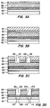
- Figs. 3A through 3E show steps in a method for forming a gate structure. Corresponding components in these figures are identified in the same way.
- the elements of the gate are formed in a silicon substrate 82 upon which are layers 84, 86, 88 and 90 of doped polysilicon, a conductive sillicide, nitride or oxide and a layer of polysilicon having a thickness of 0.02 um to 0.15 um inclusive.
- a layer 92 of resist is formed on the polysilicon layer 90 and is formed into a resist mask having openings such as shown at 94 and 96 of Fig. 3C for identifying the locations of gate conductors.
- Gasses such as HBR, HCL or SF 6 are introduced into the openings 94 and 96 so as to etch apertures 98 and 100 in the polysilicon layer 90.
- Excess materials outside gate conductors such as 102 and 104 shown in Fig. 3D are formed in the layer 88 of nitride or oxide using one of CHF 3 /CF 4 and C 4 F 8 /CF 4 ionized gasses, and the photo resist mask structure in the layer 92 is removed. Then the etching is continued down to substrate 82 as indicated by the dashed lines 106, 108, 110 and 112 so as to sacrifice the polysilicon mask in the layer 90.
Landscapes
- Internal Circuitry In Semiconductor Integrated Circuit Devices (AREA)
- Drying Of Semiconductors (AREA)
- Electrodes Of Semiconductors (AREA)
Applications Claiming Priority (2)
| Application Number | Priority Date | Filing Date | Title |
|---|---|---|---|
| US618161 | 1996-03-19 | ||
| US08/618,161 US6008121A (en) | 1996-03-19 | 1996-03-19 | Etching high aspect contact holes in solid state devices |
Publications (2)
| Publication Number | Publication Date |
|---|---|
| EP0797242A2 true EP0797242A2 (fr) | 1997-09-24 |
| EP0797242A3 EP0797242A3 (fr) | 1997-11-26 |
Family
ID=24476564
Family Applications (1)
| Application Number | Title | Priority Date | Filing Date |
|---|---|---|---|
| EP97103150A Ceased EP0797242A3 (fr) | 1996-03-19 | 1997-02-26 | Gravure des trous de contact à haut facteur de forme dans des composants à l'état solide |
Country Status (5)
| Country | Link |
|---|---|
| US (1) | US6008121A (fr) |
| EP (1) | EP0797242A3 (fr) |
| JP (1) | JPH1032250A (fr) |
| KR (1) | KR100458360B1 (fr) |
| TW (1) | TW357445B (fr) |
Cited By (4)
| Publication number | Priority date | Publication date | Assignee | Title |
|---|---|---|---|---|
| US5928967A (en) * | 1996-06-10 | 1999-07-27 | International Business Machines Corporation | Selective oxide-to-nitride etch process using C4 F8 /CO/Ar |
| WO2000003432A1 (fr) * | 1998-07-09 | 2000-01-20 | Applied Materials, Inc. | Procede de gravure au plasma d'une structure multicouche dielectrique utile notamment dans le double damasquinage |
| DE10229188A1 (de) * | 2002-06-28 | 2004-01-29 | Infineon Technologies Ag | Verfahren zur Herstellung von Kontakten zu Teilen eines in einem Halbleitersubstrat integrierten Bauelementes |
| CN103972154A (zh) * | 2013-02-01 | 2014-08-06 | 中芯国际集成电路制造(上海)有限公司 | 插塞的形成方法 |
Families Citing this family (11)
| Publication number | Priority date | Publication date | Assignee | Title |
|---|---|---|---|---|
| US7804115B2 (en) | 1998-02-25 | 2010-09-28 | Micron Technology, Inc. | Semiconductor constructions having antireflective portions |
| US6274292B1 (en) | 1998-02-25 | 2001-08-14 | Micron Technology, Inc. | Semiconductor processing methods |
| US6281100B1 (en) | 1998-09-03 | 2001-08-28 | Micron Technology, Inc. | Semiconductor processing methods |
| US6268282B1 (en) | 1998-09-03 | 2001-07-31 | Micron Technology, Inc. | Semiconductor processing methods of forming and utilizing antireflective material layers, and methods of forming transistor gate stacks |
| US6162728A (en) * | 1998-12-18 | 2000-12-19 | Texas Instruments Incorporated | Method to optimize copper chemical-mechanical polishing in a copper damascene interconnect process for integrated circuit applications |
| US6828683B2 (en) | 1998-12-23 | 2004-12-07 | Micron Technology, Inc. | Semiconductor devices, and semiconductor processing methods |
| US6147007A (en) * | 1999-06-11 | 2000-11-14 | United Microelectronics Corp. | Method for forming a contact hole on a semiconductor wafer |
| US7067414B1 (en) | 1999-09-01 | 2006-06-27 | Micron Technology, Inc. | Low k interlevel dielectric layer fabrication methods |
| US6440860B1 (en) | 2000-01-18 | 2002-08-27 | Micron Technology, Inc. | Semiconductor processing methods of transferring patterns from patterned photoresists to materials, and structures comprising silicon nitride |
| US6461963B1 (en) | 2000-08-30 | 2002-10-08 | Micron Technology, Inc. | Utilization of disappearing silicon hard mask for fabrication of semiconductor structures |
| JP3543968B1 (ja) * | 2003-01-31 | 2004-07-21 | 沖電気工業株式会社 | 半導体装置の製造方法 |
Citations (3)
| Publication number | Priority date | Publication date | Assignee | Title |
|---|---|---|---|---|
| US5173442A (en) * | 1990-07-23 | 1992-12-22 | Microelectronics And Computer Technology Corporation | Methods of forming channels and vias in insulating layers |
| US5354711A (en) * | 1990-06-26 | 1994-10-11 | Commissariat A L'energie Atomique | Process for etching and depositing integrated circuit interconnections and contacts |
| US5468342A (en) * | 1994-04-28 | 1995-11-21 | Cypress Semiconductor Corp. | Method of etching an oxide layer |
Family Cites Families (18)
| Publication number | Priority date | Publication date | Assignee | Title |
|---|---|---|---|---|
| US4461672A (en) * | 1982-11-18 | 1984-07-24 | Texas Instruments, Inc. | Process for etching tapered vias in silicon dioxide |
| US4473435A (en) * | 1983-03-23 | 1984-09-25 | Drytek | Plasma etchant mixture |
| US4631806A (en) * | 1985-05-22 | 1986-12-30 | Gte Laboratories Incorporated | Method of producing integrated circuit structures |
| US5208067A (en) * | 1986-04-14 | 1993-05-04 | International Business Machines Corporation | Surface modification of organic materials to improve adhesion |
| US5532143A (en) * | 1987-08-07 | 1996-07-02 | The Medical Research Council | Isolated DNA molecules for intergration site independent gene expression in mammalian host cells |
| JPH0817180B2 (ja) * | 1989-06-27 | 1996-02-21 | 株式会社東芝 | 半導体装置の製造方法 |
| EP0416809A3 (en) * | 1989-09-08 | 1991-08-07 | American Telephone And Telegraph Company | Reduced size etching method for integrated circuits |
| US5279990A (en) * | 1990-03-02 | 1994-01-18 | Motorola, Inc. | Method of making a small geometry contact using sidewall spacers |
| FR2664095B1 (fr) * | 1990-06-28 | 1993-12-17 | Commissariat A Energie Atomique | Procede de fabrication d'un contact electrique sur un element actif d'un circuit integre mis. |
| JP2957669B2 (ja) * | 1990-09-28 | 1999-10-06 | 株式会社東芝 | 反射マスク及びこれを用いた荷電ビーム露光装置 |
| NL9100094A (nl) * | 1991-01-21 | 1992-08-17 | Koninkl Philips Electronics Nv | Halfgeleiderinrichting en werkwijze ter vervaardiging van een dergelijke halfgeleiderinrichting. |
| US5182787A (en) * | 1991-04-29 | 1993-01-26 | At&T Bell Laboratories | Optical waveguide structure including reflective asymmetric cavity |
| EP0554123A1 (fr) * | 1992-01-31 | 1993-08-04 | STMicroelectronics, Inc. | Procédé de fabrication d'un contact |
| KR950000660B1 (ko) * | 1992-02-29 | 1995-01-27 | 현대전자산업 주식회사 | 고집적 소자용 미세콘택 형성방법 |
| DE4219213C2 (de) * | 1992-06-12 | 1995-04-20 | Loehr & Bromkamp Gmbh | Lageranordnung für eine Radnaben-Gleichlaufdrehgelenk-Einheit |
| JP2901423B2 (ja) * | 1992-08-04 | 1999-06-07 | 三菱電機株式会社 | 電界効果トランジスタの製造方法 |
| US5607879A (en) * | 1995-06-28 | 1997-03-04 | Taiwan Semiconductor Manufacturing Company Ltd. | Method for forming buried plug contacts on semiconductor integrated circuits |
| US5550085A (en) * | 1995-09-07 | 1996-08-27 | Winbond Electronics Corp. | Method for making a buried contact |
-
1996
- 1996-03-19 US US08/618,161 patent/US6008121A/en not_active Expired - Lifetime
-
1997
- 1997-02-26 EP EP97103150A patent/EP0797242A3/fr not_active Ceased
- 1997-03-11 TW TW086102987A patent/TW357445B/zh not_active IP Right Cessation
- 1997-03-12 JP JP9056758A patent/JPH1032250A/ja not_active Withdrawn
- 1997-03-19 KR KR1019970009250A patent/KR100458360B1/ko not_active Expired - Lifetime
Patent Citations (3)
| Publication number | Priority date | Publication date | Assignee | Title |
|---|---|---|---|---|
| US5354711A (en) * | 1990-06-26 | 1994-10-11 | Commissariat A L'energie Atomique | Process for etching and depositing integrated circuit interconnections and contacts |
| US5173442A (en) * | 1990-07-23 | 1992-12-22 | Microelectronics And Computer Technology Corporation | Methods of forming channels and vias in insulating layers |
| US5468342A (en) * | 1994-04-28 | 1995-11-21 | Cypress Semiconductor Corp. | Method of etching an oxide layer |
Non-Patent Citations (1)
| Title |
|---|
| KAANTA C.W. ET AL: "Dual Damascene: A ULSI wiring technology", IEEE VMIV CONFERENCE, 11 June 1991 (1991-06-11) - 12 June 1991 (1991-06-12), SANTA CLARA, USA, pages 144 - 152, XP010040523, DOI: doi:10.1109/VMIC.1991.152978 * |
Cited By (8)
| Publication number | Priority date | Publication date | Assignee | Title |
|---|---|---|---|---|
| US5928967A (en) * | 1996-06-10 | 1999-07-27 | International Business Machines Corporation | Selective oxide-to-nitride etch process using C4 F8 /CO/Ar |
| WO2000003432A1 (fr) * | 1998-07-09 | 2000-01-20 | Applied Materials, Inc. | Procede de gravure au plasma d'une structure multicouche dielectrique utile notamment dans le double damasquinage |
| US6211092B1 (en) | 1998-07-09 | 2001-04-03 | Applied Materials, Inc. | Counterbore dielectric plasma etch process particularly useful for dual damascene |
| US6399511B2 (en) | 1998-07-09 | 2002-06-04 | Applied Materials, Inc. | Plasma etch process in a single inter-level dielectric etch |
| DE10229188A1 (de) * | 2002-06-28 | 2004-01-29 | Infineon Technologies Ag | Verfahren zur Herstellung von Kontakten zu Teilen eines in einem Halbleitersubstrat integrierten Bauelementes |
| US7396749B2 (en) | 2002-06-28 | 2008-07-08 | Infineon Technologies Ag | Method for contacting parts of a component integrated into a semiconductor substrate |
| CN103972154A (zh) * | 2013-02-01 | 2014-08-06 | 中芯国际集成电路制造(上海)有限公司 | 插塞的形成方法 |
| CN103972154B (zh) * | 2013-02-01 | 2017-04-05 | 中芯国际集成电路制造(上海)有限公司 | 插塞的形成方法 |
Also Published As
| Publication number | Publication date |
|---|---|
| TW357445B (en) | 1999-05-01 |
| EP0797242A3 (fr) | 1997-11-26 |
| US6008121A (en) | 1999-12-28 |
| JPH1032250A (ja) | 1998-02-03 |
| KR100458360B1 (ko) | 2005-02-05 |
Similar Documents
| Publication | Publication Date | Title |
|---|---|---|
| US6033980A (en) | Method of forming submicron contacts and vias in an integrated circuit | |
| US6008121A (en) | Etching high aspect contact holes in solid state devices | |
| US6180517B1 (en) | Method of forming submicron contacts and vias in an integrated circuit | |
| KR100482029B1 (ko) | 엠아이엠 캐패시터 형성방법 | |
| US6878637B2 (en) | Method for fabricating semiconductor device capable of improving process margin of self align contact | |
| US7259087B2 (en) | Semiconductor devices having a via hole and methods for forming a via hole in a semiconductor device | |
| KR100275340B1 (ko) | 반도체소자의콘택홀형성방법 | |
| US5994223A (en) | Method of manufacturing analog semiconductor device | |
| KR0161878B1 (ko) | 반도체장치의 콘택홀 형성방법 | |
| KR100533363B1 (ko) | 반도체소자의 저장전극 형성방법 | |
| KR100598308B1 (ko) | 반도체 소자의 다마신 패턴 형성방법 | |
| KR0140733B1 (ko) | 반도체소자의 미세콘택 형성방법 | |
| KR100682167B1 (ko) | 금속 배선 형성 방법 | |
| KR100399963B1 (ko) | 반도체 장치의 전하저장전극 형성방법 | |
| KR100209279B1 (ko) | 반도체 소자의 콘택홀 형성방법 | |
| KR100338605B1 (ko) | 반도체디바이스의콘택홀형성방법 | |
| JPH0590420A (ja) | 接続孔の形成方法 | |
| KR100780616B1 (ko) | 반도체 소자의 제조 방법 | |
| KR100529440B1 (ko) | 반도체 소자의 금속 배선 형성 방법 | |
| KR930008893B1 (ko) | 메모리 셀의 캐패시터 제조방법 | |
| KR0126887B1 (ko) | 반도체 소자의 콘택홀 형성 방법 | |
| KR950014268B1 (ko) | 콘택형성방법 | |
| KR0172774B1 (ko) | 반도체 소자의 접촉창 형성방법 | |
| KR100328824B1 (ko) | 커패시터 제조방법 | |
| KR20000026810A (ko) | 반도체 소자의 미세 패턴 형성방법 |
Legal Events
| Date | Code | Title | Description |
|---|---|---|---|
| PUAI | Public reference made under article 153(3) epc to a published international application that has entered the european phase |
Free format text: ORIGINAL CODE: 0009012 |
|
| AK | Designated contracting states |
Kind code of ref document: A2 Designated state(s): DE FR GB IT |
|
| PUAL | Search report despatched |
Free format text: ORIGINAL CODE: 0009013 |
|
| RHK1 | Main classification (correction) |
Ipc: H01L 21/311 |
|
| AK | Designated contracting states |
Kind code of ref document: A3 Designated state(s): DE FR GB IT |
|
| 17P | Request for examination filed |
Effective date: 19980519 |
|
| 17Q | First examination report despatched |
Effective date: 20010814 |
|
| RAP1 | Party data changed (applicant data changed or rights of an application transferred) |
Owner name: INTERNATIONAL BUSINESS MACHINES CORPORATION Owner name: INFINEON TECHNOLOGIES AG |
|
| STAA | Information on the status of an ep patent application or granted ep patent |
Free format text: STATUS: THE APPLICATION HAS BEEN REFUSED |
|
| 18R | Application refused |
Effective date: 20070610 |