EP0797256A2 - Drei- oder Vier-Band-multispektrale Strukturen mit zwei gleichzeitigen Ausgangssignalen - Google Patents
Drei- oder Vier-Band-multispektrale Strukturen mit zwei gleichzeitigen Ausgangssignalen Download PDFInfo
- Publication number
- EP0797256A2 EP0797256A2 EP97301825A EP97301825A EP0797256A2 EP 0797256 A2 EP0797256 A2 EP 0797256A2 EP 97301825 A EP97301825 A EP 97301825A EP 97301825 A EP97301825 A EP 97301825A EP 0797256 A2 EP0797256 A2 EP 0797256A2
- Authority
- EP
- European Patent Office
- Prior art keywords
- layer
- radiation
- comprised
- type
- electrical conductivity
- Prior art date
- Legal status (The legal status is an assumption and is not a legal conclusion. Google has not performed a legal analysis and makes no representation as to the accuracy of the status listed.)
- Granted
Links
Images



Classifications
-
- H—ELECTRICITY
- H10—SEMICONDUCTOR DEVICES; ELECTRIC SOLID-STATE DEVICES NOT OTHERWISE PROVIDED FOR
- H10F—INORGANIC SEMICONDUCTOR DEVICES SENSITIVE TO INFRARED RADIATION, LIGHT, ELECTROMAGNETIC RADIATION OF SHORTER WAVELENGTH OR CORPUSCULAR RADIATION
- H10F77/00—Constructional details of devices covered by this subclass
- H10F77/10—Semiconductor bodies
- H10F77/14—Shape of semiconductor bodies; Shapes, relative sizes or dispositions of semiconductor regions within semiconductor bodies
- H10F77/146—Superlattices; Multiple quantum well structures
-
- B—PERFORMING OPERATIONS; TRANSPORTING
- B82—NANOTECHNOLOGY
- B82Y—SPECIFIC USES OR APPLICATIONS OF NANOSTRUCTURES; MEASUREMENT OR ANALYSIS OF NANOSTRUCTURES; MANUFACTURE OR TREATMENT OF NANOSTRUCTURES
- B82Y20/00—Nanooptics, e.g. quantum optics or photonic crystals
-
- H—ELECTRICITY
- H10—SEMICONDUCTOR DEVICES; ELECTRIC SOLID-STATE DEVICES NOT OTHERWISE PROVIDED FOR
- H10F—INORGANIC SEMICONDUCTOR DEVICES SENSITIVE TO INFRARED RADIATION, LIGHT, ELECTROMAGNETIC RADIATION OF SHORTER WAVELENGTH OR CORPUSCULAR RADIATION
- H10F39/00—Integrated devices, or assemblies of multiple devices, comprising at least one element covered by group H10F30/00, e.g. radiation detectors comprising photodiode arrays
- H10F39/10—Integrated devices
- H10F39/12—Image sensors
- H10F39/18—Complementary metal-oxide-semiconductor [CMOS] image sensors; Photodiode array image sensors
- H10F39/184—Infrared image sensors
- H10F39/1847—Multispectral infrared image sensors having a stacked structure, e.g. NPN, NPNPN or multiple quantum well [MQW] structures
Definitions
- This invention relates generally to solid state radiation detectors and, in particular, to radiation detectors that are sensitive to radiation within a plurality of spectral bands or "colors".
- a desirable type of photodetector is a two-color infrared radiation (IR) detector having simultaneous sensitivity in two spectral bands.
- the spectral bands may include short wavelength IR (SWIR), medium wavelength IR (MWIR), long wavelength IR (LWIR), and very long wavelength IR (VLWIR).
- SWIR short wavelength IR
- MWIR medium wavelength IR
- LWIR long wavelength IR
- VLWIR very long wavelength IR
- An array of two color IR detectors may be employed in a number of imaging applications wherein it is required to simultaneously detect radiation within two spectral bands from a scene within a field of view of the array.
- the array may be responsive to LWIR and MWIR, or to LWIR and SWIR.
- Fig. 1 illustrates a two-color detector of type similar to that disclosed in commonly assigned U.S. Patent No. 5,113,076, issued 5/12/92, entitled "Two Terminal Multi-band Infrared Radiation Detector" to E. F. Schulte.
- This commonly assigned patent discloses a radiation detector having two heterojunctions that function in a manner analogous to two back-to-back photodiodes. Each of the photodiodes is responsive to radiation within a different IR spectral band, such as LWIR and MWIR. Detection of a particular wavelength band is achieved by switching a bias supply.
- Disclosed configurations include an n-p-n configuration, a p-n-p configuration, and a p-n-p-n configuration.
- n-p+-n dual-band detector described by J.M. Arias et al. in the Journal of Applied Physics, 70(8), 15 October 1991, pps. 4820-4822.
- MWIR absorption occurs in the bottom n-type layer
- LWIR absorption occurs in the top n-type layer.
- an infrared detector comprised of n-type HgCdTe having electrodes 2 and 3 arranged on opposite surfaces. A polarity of a bias voltage is switchably coupled to the electrodes 2 and 3. This device is said to enable rays of wide wavelength ranges to be detected by only one semiconductor detector.
- IR-responsive materials may be found in an article entitled "HgCdTe and Related Alloys", D. Long and J.L. Schmit, Semiconductors and Semimetals, Vol. 5, IR Detectors, Academic Press 1970.
- Optical sensors that are responsive to three or more wavelengths have conventionally required beamsplitters and separate optics for each band of wavelengths.
- the use of these addition components increases the mass, volume, complexity, and cost of the optical sensor.
- each unit cell includes a bias-selectable two color detector in combination with a second bias-selectable two color detector or a single photodetector.
- Each unit cell is thus capable of simultaneously outputting charge carriers resulting from the absorption of electromagnetic radiation within two spectral bands selected from either four or three bands.
- a radiation detector that is responsive to electromagnetic radiation within a plurality of spectral bands includes a multilayered semiconductor structure forming a first two color bias-selectable photodetector comprised of a first photoresponsive diode having a first terminal electrically coupled in series with a first terminal of a second photoresponsive diode.
- the first photoresponsive diode is responsive to electromagnetic radiation within a first predetermined band of wavelengths and the second photoresponsive diode is responsive to electromagnetic radiation within a second predetermined band of wavelengths.
- the multilayered semiconductor structure further forms at least one further photodetector having at least one further photoresponsive diode having a first terminal coupled in series with a second terminal of the second photoresponsive diode.
- the at least one further photoresponsive diode is responsive to electromagnetic radiation within a third predetermined band of wavelengths.
- the unit cells in accordance with this invention are three terminal devices, and a first electrical contact is conductively coupled to the second terminal of the first photoresponsive diode; a second electrical contact is conductively coupled to the second terminal of the second photoresponsive diode and to the first terminal of the further photoresponsive diode; and a third electrical contact is conductively coupled to a second terminal of the further photoresponsive diode.
- One of the layers prevents photocarriers generated in the second photoresponsive diode from being collected by the at least one further photoresponsive diode, and also prevents photocarriers generated in the at least one further photodiode from being collected by the second photoresponsive diode.
- the layer is interposed between the first terminal of the at least one further photodiode and the second terminal of the second photoresponsive diode.
- SWIR radiation is considered to include a spectral region extending from approximately 1000 nanometers (nm) to approximately 3000 nm.
- Medium Wavelength Infrared (MWIR) radiation is considered to include a spectral region extending from approximately 3000 nm to approximately 8000 nm.
- Long Wavelength Infrared (LWIR) radiation is considered to include a spectral region extending from approximately 7000 nm to approximately 14000 nm.
- Very Long Wavelength Infrared (VLWIR) radiation is considered to include a spectral region extending from approximately 12000 nm to approximately 30000 nm.
- the radiation detectors disclosed herein may be fabricated by Liquid Phase Epitaxy (LPE). Suitable LPE growth techniques are described in the following two articles: T. Tung, M.H. Kalisher, A.P. Stevens and P.E. Herning, in: Materials for Infrared Detectors and Sources, Mater. Res. Soc. Symp. Proc., Vol. 90 (Mater. Res. Soc., Pittsburgh, PA, 1987), p.321; and T. Tung, Infinite-Melt Vertical Liquid-Phase Epitaxy of HgCdTe from Hg Solution: Status and Prospects, J. Crystal Growth 86 (1988), pps. 161-172.
- LPE Liquid Phase Epitaxy
- MBE Molecular Beam Epitaxy
- Figs. 2A and 3A for showing a first embodiment of a four color IR-responsive radiation detector 10 in accordance with this invention.
- the detector 10 occupies a radiation detector unit cell area and comprises four photodetectors D1-D4.
- the various layer thicknesses described below are for the LPE-grown case. If MBE is employed then the layer thicknesses may be reduced accordingly.
- a detector array is comprised of a plurality of such photodetector unit cells, each of which defines a detector site or pixel.
- the enlarged cross-sectional view of Fig. 2A is of a four color detector that corresponds to the schematic diagram of Fig. 3A. Modifications to this structure to obtain the first embodiment of the three color detector of Figs. 2B and 3B are described below.
- the detector 10 is formed over a transparent substrate 12 (transparent at wavelengths ⁇ 1 - ⁇ 4 of interest), e.g., a Group II-VI material such CdZnTe.
- the substrate 12 can also be comprised of a material other than a Group II-VI material, such as a Group IV material, such as Si, or a Group III-V material, such as GaAs.
- Layer 14 has a thickness in a range of, by example, 8-10 micrometers and is doped n-type with, by example, indium at a concentration of approximately 3x10 15 atoms/cm 3 .
- a p + layer 16 having an energy bandgap giving it a cut-off wavelength ⁇ c that is less than ⁇ c1 .
- Layer 16 has a thickness in a range of, by example, 3-4 micrometers and is doped p-type with, by example, arsenic.
- Layer 18 has a thickness in a range of 8-10 micrometers and is doped n-type with, by example, indium at a concentration of approximately 3x10 15 atoms/cm 3 .
- n + layer 20 having an energy bandgap giving it a cut-off wavelength ⁇ c that is less than ⁇ c2 .
- Layer 20 has a thickness in a range of 3-4 micrometers and is n-type.
- Layer 22 has a thickness in a range of 8-10 micrometers and is doped n-type with, by example, indium at a concentration of approximately 3x10 15 atoms/cm 3 .
- a p + layer 24 having an energy bandgap giving it a cut-off wavelength ⁇ c that is less than ⁇ c3 .
- Layer 24 also has a thickness in a range of 3-4 micrometers and is doped p-type with, by example, arsenic.
- ⁇ c4 n-type fourth color
- ⁇ c4 n-type fourth color
- Layer 26 has a thickness comparable to that of the layers 14, 18 and 22 and is doped n-type with, by example, indium at a concentration of approximately 3x10 15 atoms/cm 3 .
- the multi-layered structure is differentiated with orthogonally disposed trenches to form a plurality of mesa structures, and the optically active volume of each detector 10 is contained within one of the mesa structures.
- the mesa structure has a top surface 10a and downwardly sloping sidewalls 10b that terminate at the surface of the substrate 12.
- Contact metalization or terminals 28, 30, and 32 in combination with a suitable interconnect system such as indium bumps (not shown), are provided for coupling the mesa structure to external biasing and read-out electronics which, in a FPA array embodiment, will typically be a readout integrated circuit.
- a suitable interconnect system such as indium bumps (not shown)
- indium bump interconnects enable the array to be subsequently hybridized with the associated readout integrated circuit by cold-welding the indium bumps to corresponding indium bumps on a surface of the readout integrated circuit.
- Techniques for hybridizing radiation detector arrays to readout integrated circuits are known in the art.
- the n + layer 20 functions as an electrically common layer, and further functions as a wide-bandgap barrier layer that separates minority carriers generated in the third (cutoff ⁇ c2 ) and fifth (cutoff ⁇ c3 ) layers and guides them to the proper collecting p-n junction. That is, photocarriers generated in the layer 18 are inhibited from crossing into the layer 22, and are instead collected by the p-n junction at the interface between the layers 18/16. In like manner, photocarriers generated in the layer 22 are inhibited from crossing into the layer 18, and are instead collected by the p-n junction at the interface between the layers 22/24.
- An electrically insulating dielectric layer preferably a wide-bandgap passivation layer, such as a layer of CdTe, can be applied over exposed surfaces 10a and 10b of the mesa structures.
- the passivation layer beneficially reduces surface states and improves the signal-to-noise ratio of the detector 10.
- Suitable bias arrangements for the embodiment shown in Figs. 2A and 3A are terminal 32 being biased at ⁇ 50 mV with respect to terminal 30, and terminal 28 being biased at ⁇ 50 mV with respect to terminal 30.
- terminal 32 is positive with respect to terminal 30, which in turn is positive with respect to terminal 28, then a photocurrent induced by ⁇ c4 can be obtained at terminal 32, a photocurrent induced by ⁇ c2 can be obtained at terminal 28, and a photocurrent representing a difference between ⁇ c4 and ⁇ c2 can be obtained at terminal 30.
- terminal 30 is made negative with respect to terminal 28, then a photocurrent representing a sum of ⁇ c4 and ⁇ c1 can be obtained at terminal 30.
- the structure is substantially identical to that of the four photodetector embodiment of Fig. 2A.
- the most significant exception is that the layer 26 is not provided, and the terminal 32 is electrically coupled to the layer 24.
- the upper photodiode (layers 22 and 24) could be reversed (i.e., the anode could be adjacent to the common layer 20), by reversing the order of the n and p + layers 22 and 24.
- the common terminal 30 is connected to both layers 20 and 22.
- the resulting multispectral device structures are capable of detection in three bands (Fig. 3B) or four bands (Fig. 3A).
- a bias-switched, two-terminal, two color detector structure is provided (layers 14-18), and on top of this structure is placed either a third photodiode (Fig. 3B), or a second bias-switched two color detector (Fig. 3A).
- the polarity of the bias potentials (+V B , -V B ) selects the spectral sensitivities of the device, because only the reverse-biased p-n junction collects photogenerated carriers.
- the four color detector 10 thus operates as two independent bias-selectable devices that occupy a same FPA unit cell. In the three color detector 10' of Fig. 3B only the bottom detector structure has a bias-selectable spectral sensitivity.
- the third photodiode in the embodiment Fig. 3B, and also the second two color detector of Fig. 3A, are separated from the underlying bias switched two color detector by the wider bandgap common layer 20.
- both detectors 10 and 10' require only two indium bumps within each pixel (for terminals 28 and 32 in Fig. 3A and terminals 28 and 32 of Fig. 3B), and are thus compatible with conventional readout circuit architectures.
- the common terminal 30 can be coupled to metalization that is located within and runs though the array, with electrical contact being made at one or more locations at the periphery of the array (and thence away from the optically active area).
- the common terminal is terminal 30
- the third band output current is always available at terminal 32, while at terminal 28 either the first band or the second band photocurrent is selected by appropriately changing the relative bias between terminals 28 and 30.
- the signal at terminal 32 can be switched between the third and fourth bands by changing the bias at terminal 32 relative to terminal 30.
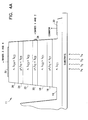
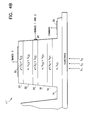
- Figs. 4A, 4B, 5A and 5B for illustrating second embodiments of the four color and three color detectors, designated 11 and 11', respectively.
- the multi-layered structure is differentiated with orthogonally disposed trenches to form the plurality of mesa structures.
- each mesa structure has downwardly sloping sidewalls that terminate in the n-type layer 14, instead of at the surface of the substrate 12.
- the terminals 28 and 30 are also rearranged such that the common terminal 30 is coupled to the n-type layer 14, which then forms a common contact layer for all of the photodetectors of the array. Referring also to Figs.
- the bias sources are now referenced to the common contact layer 14.
- the photodetectors 11 and 11' are identical to the photodetectors 10 and 10' of Figs. 2A and 2B, respectively.
- One advantage to the structures shown in Figs. 4A and 4B is that generally larger arrays (i.e., more photodetectors) can be fabricated than for the embodiments of Figs. 2A and 2B.
- the photodetectors 10, 10', 11 and 11' can be constructed to be responsive to a number of combinations of wavelength bands, such as SWIR/MWIR/LWIR/VLWIR (photodetectors 10 and 11), SWIR/MWIR/LWIR (photodetectors 10' and 11'), and MWIR 1 /MWIR 2 /VLWIR, wherein MWIR 1 includes a wavelength in the range of, by example, 4000 nm to 5000 nm, and where MWIR 2 includes a wavelength in the range of, by example, 6000 nm to 7000 nm.
- the arrangement of the radiation absorbing layers in these various embodiments is such that the incident radiation first encounters the wider bandgap semiconductor material, and that the bandgap of the succeeding layers becomes narrower.
Landscapes
- Chemical & Material Sciences (AREA)
- Engineering & Computer Science (AREA)
- Nanotechnology (AREA)
- Physics & Mathematics (AREA)
- Life Sciences & Earth Sciences (AREA)
- Biophysics (AREA)
- Optics & Photonics (AREA)
- Crystallography & Structural Chemistry (AREA)
- Light Receiving Elements (AREA)
- Photometry And Measurement Of Optical Pulse Characteristics (AREA)
- Solid State Image Pick-Up Elements (AREA)
Applications Claiming Priority (2)
| Application Number | Priority Date | Filing Date | Title |
|---|---|---|---|
| US618136 | 1996-03-19 | ||
| US08/618,136 US5731621A (en) | 1996-03-19 | 1996-03-19 | Three band and four band multispectral structures having two simultaneous signal outputs |
Publications (3)
| Publication Number | Publication Date |
|---|---|
| EP0797256A2 true EP0797256A2 (de) | 1997-09-24 |
| EP0797256A3 EP0797256A3 (de) | 1998-08-05 |
| EP0797256B1 EP0797256B1 (de) | 2003-04-23 |
Family
ID=24476462
Family Applications (1)
| Application Number | Title | Priority Date | Filing Date |
|---|---|---|---|
| EP97301825A Expired - Lifetime EP0797256B1 (de) | 1996-03-19 | 1997-03-18 | Drei- oder Vier-Band-multispektrale Strukturen mit zwei gleichzeitigen Ausgangssignalen |
Country Status (5)
| Country | Link |
|---|---|
| US (1) | US5731621A (de) |
| EP (1) | EP0797256B1 (de) |
| JP (1) | JP3124732B2 (de) |
| DE (1) | DE69721112T2 (de) |
| IL (1) | IL120365A (de) |
Cited By (9)
| Publication number | Priority date | Publication date | Assignee | Title |
|---|---|---|---|---|
| EP1265296A1 (de) * | 2001-06-08 | 2002-12-11 | Zarlink Semiconductor AB | Optischer Dektektor mit integriertem Filter |
| WO2004107378A3 (en) * | 2003-05-22 | 2005-03-24 | Itt Mfg Enterprises Inc | Tuned bandwidth photocathode for transmission electron affinity devices |
| WO2005122261A1 (en) * | 2004-06-10 | 2005-12-22 | Bae Systems Plc | Two colour photon detector |
| WO2005101512A3 (fr) * | 2004-04-05 | 2006-07-20 | Commissariat Energie Atomique | Circuit de detection photonique a structure mesa |
| WO2007068970A3 (en) * | 2005-12-14 | 2007-07-26 | Selex Sensors & Airborne Sys | Multi colour photon detectors |
| WO2009040270A3 (en) * | 2007-09-24 | 2009-05-22 | Selex Sensors & Airborne Sys | Two colour photon detector |
| CN104332523A (zh) * | 2014-08-15 | 2015-02-04 | 中国空空导弹研究院 | 一种基于石墨烯的三模复合探测器 |
| WO2015130351A1 (en) * | 2014-02-27 | 2015-09-03 | Raytheon Company | Simultaneous dual-band detector |
| CN108281495A (zh) * | 2018-01-05 | 2018-07-13 | 北京和炬科技有限责任公司 | 一种GaSb基背靠背结构四波段红外探测器及制备方法 |
Families Citing this family (36)
| Publication number | Priority date | Publication date | Assignee | Title |
|---|---|---|---|---|
| FR2756666B1 (fr) * | 1996-12-04 | 1999-02-19 | Thomson Csf | Detecteur d'ondes electromagnetiques |
| FR2756667B1 (fr) * | 1996-12-04 | 1999-02-19 | Thomson Csf | Detecteur d'ondes electromagnetiques bispectral |
| JP4032454B2 (ja) * | 1997-06-27 | 2008-01-16 | ソニー株式会社 | 三次元回路素子の製造方法 |
| US6043550A (en) | 1997-09-03 | 2000-03-28 | Sumitomo Electric Industries, Ltd. | Photodiode and photodiode module |
| KR100253660B1 (ko) * | 1997-09-13 | 2000-04-15 | 최동환 | 이색 적외선 검출소자의 구조 및 제조방법 |
| US6111300A (en) * | 1998-12-01 | 2000-08-29 | Agilent Technologies | Multiple color detection elevated pin photo diode active pixel sensor |
| US7554586B1 (en) | 1999-10-20 | 2009-06-30 | Rochester Institute Of Technology | System and method for scene image acquisition and spectral estimation using a wide-band multi-channel image capture |
| US6455908B1 (en) * | 2001-03-09 | 2002-09-24 | Applied Optoelectronics, Inc. | Multispectral radiation detectors using strain-compensating superlattices |
| US6885002B1 (en) | 2001-08-31 | 2005-04-26 | Raytheon Company | IRFPA ROIC with dual TDM reset integrators and sub-frame averaging functions per unit cell |
| US6803557B1 (en) | 2002-09-27 | 2004-10-12 | Raytheon Company | Photodiode having voltage tunable spectral response |
| AT414053B (de) * | 2003-10-08 | 2006-08-15 | Efkon Ag | Infrarot (ir)-empfangseinrichtung |
| US7053998B2 (en) * | 2003-12-22 | 2006-05-30 | Searete Llc | Photo-detector filter |
| US7045760B2 (en) | 2003-12-19 | 2006-05-16 | Searete Llc | Intensity detector circuitry |
| US7511254B2 (en) * | 2003-12-19 | 2009-03-31 | Searete, Llc | Photo-detector filter having a cascaded low noise amplifier |
| US7129489B2 (en) * | 2004-12-03 | 2006-10-31 | Raytheon Company | Method and apparatus providing single bump, multi-color pixel architecture |
| FR2879818B1 (fr) * | 2004-12-17 | 2007-04-20 | Commissariat Energie Atomique | Photodetecteur a semi-conducteur, dispositif de detection multi-spectrale d'un rayonnement electromagnetique mettant en oeuvre un tel photodetecteur, et procede de mise en oeuvre d'un tel dispositif |
| JP4750070B2 (ja) * | 2006-04-27 | 2011-08-17 | 株式会社半導体エネルギー研究所 | 半導体装置及びそれを用いた電子機器 |
| US7755023B1 (en) * | 2007-10-09 | 2010-07-13 | Hrl Laboratories, Llc | Electronically tunable and reconfigurable hyperspectral photon detector |
| US20100012849A1 (en) * | 2008-07-21 | 2010-01-21 | United States Of America As Represented By The Administrator Of The National Aeronautics And Spac | Detector for dual band ultraviolet detection |
| US8093559B1 (en) * | 2008-12-02 | 2012-01-10 | Hrl Laboratories, Llc | Methods and apparatus for three-color infrared sensors |
| US8669588B2 (en) * | 2009-07-06 | 2014-03-11 | Raytheon Company | Epitaxially-grown position sensitive detector |
| JP2010045417A (ja) * | 2009-11-27 | 2010-02-25 | Mitsubishi Electric Corp | 半導体受光素子 |
| TWI481039B (zh) * | 2009-11-30 | 2015-04-11 | Nat Inst Chung Shan Science & Technology | Infrared sensing array device with readout circuit |
| US8559113B2 (en) * | 2009-12-10 | 2013-10-15 | Raytheon Company | Multi-spectral super-pixel filters and methods of formation |
| US8143687B2 (en) * | 2009-12-17 | 2012-03-27 | Raytheon Company | Multi-band, reduced-volume radiation detectors and methods of formation |
| US8350208B1 (en) | 2010-01-21 | 2013-01-08 | Arizona Board Of Regents, A Body Corporate Of The State Of Arizona, Acting For And On Behalf Of Arizona State University | Two-terminal multi-color photodetectors and focal plane arrays |
| US8441087B2 (en) | 2011-07-22 | 2013-05-14 | Raytheon Company | Direct readout focal plane array |
| US10115764B2 (en) | 2011-08-15 | 2018-10-30 | Raytheon Company | Multi-band position sensitive imaging arrays |
| US9184194B2 (en) | 2011-12-21 | 2015-11-10 | Arizona Board Of Regents, A Body Corporate Of The State Of Arizona, Acting For And On Behalf Of Arizona State University | Multiband photodetector utilizing serially connected unipolar and bipolar devices |
| US8941203B2 (en) * | 2012-03-01 | 2015-01-27 | Raytheon Company | Photodetector with surface plasmon resonance |
| US10014424B2 (en) * | 2014-03-13 | 2018-07-03 | Raytheon Company | Reduced junction area barrier-based photodetector |
| US9755091B2 (en) * | 2015-04-06 | 2017-09-05 | The Boeing Company | Dual-band infrared detector and method of detecting multiple bands of infrared radiation |
| DE102017004149A1 (de) * | 2017-05-02 | 2018-11-08 | Azur Space Solar Power Gmbh | Lichtempfangseinheit |
| US11121302B2 (en) | 2018-10-11 | 2021-09-14 | SeeQC, Inc. | System and method for superconducting multi-chip module |
| IT202000018760A1 (it) * | 2020-07-31 | 2022-01-31 | Milano Politecnico | Dispositivo sensore di radiazione elettromagnetica a doppio fotodiodo |
| TWI905261B (zh) * | 2021-09-09 | 2025-11-21 | 晶元光電股份有限公司 | 光電元件 |
Family Cites Families (12)
| Publication number | Priority date | Publication date | Assignee | Title |
|---|---|---|---|---|
| JPS55101832A (en) * | 1979-01-30 | 1980-08-04 | Fujitsu Ltd | Infrared detector |
| US4582952A (en) * | 1984-04-30 | 1986-04-15 | Astrosystems, Inc. | Gallium arsenide phosphide top solar cell |
| US4753684A (en) * | 1986-10-31 | 1988-06-28 | The Standard Oil Company | Photovoltaic heterojunction structures |
| DE3710986A1 (de) * | 1987-04-01 | 1988-10-20 | Messerschmitt Boelkow Blohm | Lichtempfindliche detektorvorrichtung |
| US5322572A (en) * | 1989-11-03 | 1994-06-21 | The United States Of America As Represented By The United States Department Of Energy | Monolithic tandem solar cell |
| US5113076A (en) * | 1989-12-19 | 1992-05-12 | Santa Barbara Research Center | Two terminal multi-band infrared radiation detector |
| US5059786A (en) * | 1990-05-04 | 1991-10-22 | The United States Of America As Represented By The Secretary Of The Navy | Multi-color coincident infrared detector |
| US5149956A (en) * | 1991-06-12 | 1992-09-22 | Santa Barbara Research Center | Two-color radiation detector array and methods of fabricating same |
| US5380669A (en) * | 1993-02-08 | 1995-01-10 | Santa Barbara Research Center | Method of fabricating a two-color detector using LPE crystal growth |
| US5457331A (en) * | 1993-04-08 | 1995-10-10 | Santa Barbara Research Center | Dual-band infrared radiation detector optimized for fabrication in compositionally graded HgCdTe |
| DE19512493A1 (de) * | 1995-04-04 | 1996-10-10 | Siemens Ag | Farbsensoranordnung |
| US5581084A (en) * | 1995-06-07 | 1996-12-03 | Santa Barbara Research Center | Simultaneous two color IR detector having common middle layer metallic contact |
-
1996
- 1996-03-19 US US08/618,136 patent/US5731621A/en not_active Expired - Lifetime
-
1997
- 1997-03-03 IL IL12036597A patent/IL120365A/xx not_active IP Right Cessation
- 1997-03-18 DE DE69721112T patent/DE69721112T2/de not_active Expired - Lifetime
- 1997-03-18 EP EP97301825A patent/EP0797256B1/de not_active Expired - Lifetime
- 1997-03-19 JP JP09066525A patent/JP3124732B2/ja not_active Expired - Lifetime
Cited By (14)
| Publication number | Priority date | Publication date | Assignee | Title |
|---|---|---|---|---|
| EP1265296A1 (de) * | 2001-06-08 | 2002-12-11 | Zarlink Semiconductor AB | Optischer Dektektor mit integriertem Filter |
| WO2004107378A3 (en) * | 2003-05-22 | 2005-03-24 | Itt Mfg Enterprises Inc | Tuned bandwidth photocathode for transmission electron affinity devices |
| US6998635B2 (en) | 2003-05-22 | 2006-02-14 | Itt Manufacturing Enterprises Inc. | Tuned bandwidth photocathode for transmission negative electron affinity devices |
| US7936034B2 (en) | 2004-04-05 | 2011-05-03 | Commissariat A L'energie Atomique | Mesa structure photon detection circuit |
| WO2005101512A3 (fr) * | 2004-04-05 | 2006-07-20 | Commissariat Energie Atomique | Circuit de detection photonique a structure mesa |
| WO2005122261A1 (en) * | 2004-06-10 | 2005-12-22 | Bae Systems Plc | Two colour photon detector |
| WO2007068970A3 (en) * | 2005-12-14 | 2007-07-26 | Selex Sensors & Airborne Sys | Multi colour photon detectors |
| US7671341B2 (en) | 2005-12-14 | 2010-03-02 | Selex Sensors And Airborne Systems Limited | Multi colour photon detectors |
| WO2009040270A3 (en) * | 2007-09-24 | 2009-05-22 | Selex Sensors & Airborne Sys | Two colour photon detector |
| WO2015130351A1 (en) * | 2014-02-27 | 2015-09-03 | Raytheon Company | Simultaneous dual-band detector |
| CN104332523A (zh) * | 2014-08-15 | 2015-02-04 | 中国空空导弹研究院 | 一种基于石墨烯的三模复合探测器 |
| CN104332523B (zh) * | 2014-08-15 | 2017-01-18 | 中国空空导弹研究院 | 一种基于石墨烯的三模复合探测器 |
| CN108281495A (zh) * | 2018-01-05 | 2018-07-13 | 北京和炬科技有限责任公司 | 一种GaSb基背靠背结构四波段红外探测器及制备方法 |
| CN108281495B (zh) * | 2018-01-05 | 2020-06-05 | 北京和炬科技有限责任公司 | 一种GaSb基背靠背结构四波段红外探测器及制备方法 |
Also Published As
| Publication number | Publication date |
|---|---|
| IL120365A0 (en) | 1997-07-13 |
| DE69721112D1 (de) | 2003-05-28 |
| JPH1054757A (ja) | 1998-02-24 |
| US5731621A (en) | 1998-03-24 |
| JP3124732B2 (ja) | 2001-01-15 |
| IL120365A (en) | 2001-03-19 |
| EP0797256B1 (de) | 2003-04-23 |
| DE69721112T2 (de) | 2004-02-05 |
| EP0797256A3 (de) | 1998-08-05 |
Similar Documents
| Publication | Publication Date | Title |
|---|---|---|
| US5731621A (en) | Three band and four band multispectral structures having two simultaneous signal outputs | |
| US5959339A (en) | Simultaneous two-wavelength p-n-p-n Infrared detector | |
| US5581084A (en) | Simultaneous two color IR detector having common middle layer metallic contact | |
| US5559336A (en) | Integrated LPE-grown structure for simultaneous detection of infrared radiation in two bands | |
| EP0518243B1 (de) | Zweifarbige Strahlungsdetektoranordnung und Verfahren zu ihrer Herstellung | |
| US8044435B2 (en) | Sub-pixel nBn detector | |
| US5567975A (en) | Group II-VI radiation detector for simultaneous visible and IR detection | |
| US6455908B1 (en) | Multispectral radiation detectors using strain-compensating superlattices | |
| US5721429A (en) | Self-focusing detector pixel structure having improved sensitivity | |
| US6028323A (en) | Quantum well infared image conversion panel and associated methods | |
| US8691614B2 (en) | Direct readout focal plane array | |
| US20110101483A1 (en) | Two colour photon detector | |
| KR102863875B1 (ko) | 이중 광다이오드 전자기 방사선 센서 디바이스 | |
| EP1817802A1 (de) | Verfahren und vorrichtung zur bereitstellung von mehrfarbiger pixelarchitektur mit einem bump | |
| US10090426B2 (en) | Dark current mitigation with diffusion control | |
| US20100295141A1 (en) | Two colour photon detector | |
| Rogalski | Heterostructure HgCdTe photovoltaic detectors | |
| Rogalski | Recent progress in HgCdTe infrared detector technology | |
| WO1996010843A1 (en) | Photosensitive semiconductor array |
Legal Events
| Date | Code | Title | Description |
|---|---|---|---|
| PUAI | Public reference made under article 153(3) epc to a published international application that has entered the european phase |
Free format text: ORIGINAL CODE: 0009012 |
|
| AK | Designated contracting states |
Kind code of ref document: A2 Designated state(s): DE FR GB |
|
| PUAL | Search report despatched |
Free format text: ORIGINAL CODE: 0009013 |
|
| AK | Designated contracting states |
Kind code of ref document: A3 Designated state(s): DE FR GB |
|
| RAP1 | Party data changed (applicant data changed or rights of an application transferred) |
Owner name: RAYTHEON COMPANY |
|
| 17P | Request for examination filed |
Effective date: 19990119 |
|
| RAP1 | Party data changed (applicant data changed or rights of an application transferred) |
Owner name: RAYTHEON COMPANY |
|
| 17Q | First examination report despatched |
Effective date: 20011015 |
|
| GRAG | Despatch of communication of intention to grant |
Free format text: ORIGINAL CODE: EPIDOS AGRA |
|
| GRAG | Despatch of communication of intention to grant |
Free format text: ORIGINAL CODE: EPIDOS AGRA |
|
| GRAH | Despatch of communication of intention to grant a patent |
Free format text: ORIGINAL CODE: EPIDOS IGRA |
|
| GRAH | Despatch of communication of intention to grant a patent |
Free format text: ORIGINAL CODE: EPIDOS IGRA |
|
| GRAH | Despatch of communication of intention to grant a patent |
Free format text: ORIGINAL CODE: EPIDOS IGRA |
|
| GRAA | (expected) grant |
Free format text: ORIGINAL CODE: 0009210 |
|
| AK | Designated contracting states |
Designated state(s): DE FR GB |
|
| REG | Reference to a national code |
Ref country code: GB Ref legal event code: FG4D |
|
| REF | Corresponds to: |
Ref document number: 69721112 Country of ref document: DE Date of ref document: 20030528 Kind code of ref document: P |
|
| ET | Fr: translation filed | ||
| PLBE | No opposition filed within time limit |
Free format text: ORIGINAL CODE: 0009261 |
|
| STAA | Information on the status of an ep patent application or granted ep patent |
Free format text: STATUS: NO OPPOSITION FILED WITHIN TIME LIMIT |
|
| 26N | No opposition filed |
Effective date: 20040126 |
|
| REG | Reference to a national code |
Ref country code: FR Ref legal event code: PLFP Year of fee payment: 20 |
|
| PGFP | Annual fee paid to national office [announced via postgrant information from national office to epo] |
Ref country code: DE Payment date: 20160315 Year of fee payment: 20 |
|
| PGFP | Annual fee paid to national office [announced via postgrant information from national office to epo] |
Ref country code: FR Payment date: 20160208 Year of fee payment: 20 Ref country code: GB Payment date: 20160316 Year of fee payment: 20 |
|
| REG | Reference to a national code |
Ref country code: DE Ref legal event code: R071 Ref document number: 69721112 Country of ref document: DE |
|
| REG | Reference to a national code |
Ref country code: GB Ref legal event code: PE20 Expiry date: 20170317 |
|
| PG25 | Lapsed in a contracting state [announced via postgrant information from national office to epo] |
Ref country code: GB Free format text: LAPSE BECAUSE OF EXPIRATION OF PROTECTION Effective date: 20170317 |