EP0797280B1 - Dispositif comprenant un laser amélioré à cascade quantique - Google Patents
Dispositif comprenant un laser amélioré à cascade quantique Download PDFInfo
- Publication number
- EP0797280B1 EP0797280B1 EP97301678A EP97301678A EP0797280B1 EP 0797280 B1 EP0797280 B1 EP 0797280B1 EP 97301678 A EP97301678 A EP 97301678A EP 97301678 A EP97301678 A EP 97301678A EP 0797280 B1 EP0797280 B1 EP 0797280B1
- Authority
- EP
- European Patent Office
- Prior art keywords
- region
- laser
- active
- energy
- active region
- Prior art date
- Legal status (The legal status is an assumption and is not a legal conclusion. Google has not performed a legal analysis and makes no representation as to the accuracy of the status listed.)
- Expired - Lifetime
Links
Images
Classifications
-
- H—ELECTRICITY
- H01—ELECTRIC ELEMENTS
- H01S—DEVICES USING THE PROCESS OF LIGHT AMPLIFICATION BY STIMULATED EMISSION OF RADIATION [LASER] TO AMPLIFY OR GENERATE LIGHT; DEVICES USING STIMULATED EMISSION OF ELECTROMAGNETIC RADIATION IN WAVE RANGES OTHER THAN OPTICAL
- H01S5/00—Semiconductor lasers
- H01S5/30—Structure or shape of the active region; Materials used for the active region
- H01S5/34—Structure or shape of the active region; Materials used for the active region comprising quantum well or superlattice structures, e.g. single quantum well [SQW] lasers, multiple quantum well [MQW] lasers or graded index separate confinement heterostructure [GRINSCH] lasers
- H01S5/3401—Structure or shape of the active region; Materials used for the active region comprising quantum well or superlattice structures, e.g. single quantum well [SQW] lasers, multiple quantum well [MQW] lasers or graded index separate confinement heterostructure [GRINSCH] lasers having no PN junction, e.g. unipolar lasers, intersubband lasers, quantum cascade lasers
- H01S5/3402—Structure or shape of the active region; Materials used for the active region comprising quantum well or superlattice structures, e.g. single quantum well [SQW] lasers, multiple quantum well [MQW] lasers or graded index separate confinement heterostructure [GRINSCH] lasers having no PN junction, e.g. unipolar lasers, intersubband lasers, quantum cascade lasers intersubband lasers, e.g. transitions within the conduction or valence bands
-
- B—PERFORMING OPERATIONS; TRANSPORTING
- B82—NANOTECHNOLOGY
- B82Y—SPECIFIC USES OR APPLICATIONS OF NANOSTRUCTURES; MEASUREMENT OR ANALYSIS OF NANOSTRUCTURES; MANUFACTURE OR TREATMENT OF NANOSTRUCTURES
- B82Y20/00—Nanooptics, e.g. quantum optics or photonic crystals
Definitions
- This invention pertains to the field of semiconductor lasers. More specifically, it pertains to unipolar semiconductor lasers.
- the new laser was designated "Quantum Cascade” (QC) laser, and is based on one type of carrier (typically electrons) making transitions between energy levels created by quantum confinement.
- QC Quantum Cascade
- QC lasers comprise a multiplicity (e.g., 25) of essentially identical undoped "active regions", each active region comprising a multiplicity of semiconductor layers. Between two adjacent active regions is disposed a multilayer semiconductor region, frequently referred-to as an "injection/relaxation” (I/R) region. At least some of the layers in each I/R region are doped.
- I/R injection/relaxation
- the '709 patent discloses a QC laser that involves "diagonal" transitions, i.e., transitions between energy levels in adjacent quantum wells, with each I/R region being a digitally graded gap region.
- Exemplary QC lasers were reported to have lasing temperatures as high as 125K.
- EP-A-0676839 discloses a QC laser with modified structure. Among the modifications was a change in the active regions such that the lasing transition was a "vertical" transition, i.e., a transition from a higher to a lower energy level in a given quantum well. A further modification was incorporated in the I/R regions, with the layer structure designed such that each I/R region provided (ungraded) "minibands” and a “minigap” between the minibands (see FIG.11 of EP-A-0676839). Exemplary QC lasers according to EP-A-0676839 were found to lase at, e.g., 100°K.
- EP-A-0744801 discloses a further modification, namely, provision of a highly doped layer in the upper cladding layer of a QC laser.
- the highly doped layer resulted in lowered refractive index of the upper cladding layer and in increased confinement of the fundamental laser mode.
- the I/R region comprised an "injector" consisting of 4 coupled quantum wells which form a pseudo-quaternary alloy simulating a graded gap (see Table II of EP-A-0744801).
- EP-A-0744801 reported lasing at 130K, but the QC laser did not lase at temperatures substantially above that temperature.
- a room temperature mid-infrared QC laser that comprises a funnel injector as well as a thin quantum well in the active region that serves as a wave function-increasing feature that facilitates radiation transition of charge carriers in an adjacent quantum well.
- the QC laser comprises a multiplicity of essentially identical multilayer active regions, with a first and a second of said active regions being separated by a multilayer I/R region.
- the QC laser also comprises means for applying a voltage across the active regions with the I/R regions therebetween, such that charge carriers (typically electrons) flow (downstream) from the first active region towards the second active region.
- the first active region comprises one or more quantum wells (QWs), a first of said QWs has at least a second and a third energy state for the charge carriers, with the third energy state being higher than the second energy state.
- QWs quantum wells
- a first of said QWs has at least a second and a third energy state for the charge carriers, with the third energy state being higher than the second energy state.
- Associated with the second and third energy states are, respectively, second and third wavefunctions of charge carriers, said wavefunctions selected such that the charge carriers undergo a radiative transition from the third to the second energy state during operation of the QC
- the first active region comprises a wavefunction-increasing feature for increasing (compared to an otherwise identical comparison laser not comprising said feature) an amplitude of the third wavefunction in a first barrier layer disposed between the first QW and an I/R region immediately upstream of the first active region.
- the wavefunction-increasing feature is an appropriately placed thin QW, but could also be, for instance, an appropriately placed layer of a semiconductor material of intermediate conduction band discontinuity.
- the QC laser further comprises an upper and a lower cladding region, with the active regions disposed between the upper and lower cladding regions.
- at least the upper cladding region comprises at least one InP layer, whereby a thermal property of the QC laser is improved.
- the QC laser comprises the above discussed first and second active regions with a I/R region therebetween.
- the I/R region is selected to provide a miniband having an energy width, and is furthermore selected to provide a minigap above the miniband in energy.
- the minigap is selected to substantially prevent escape of charge carriers from the third energy state into the energy continuum, and the miniband is selected to facilitate removal of charge carriers from a non-lasing lower energy level.
- the I/R region furthermore is selected such that the energy width of the miniband decreases over at least a portion of the distance from the first to the second active region, said portion including the contact between the I/R region and the second active region.
- QC lasers according to the invention typically have a maximum lasing temperature above 260K, preferably 300K or more.
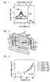
- FIG. 1 shows data on optical power vs. bias current that demonstrates that a QC laser that can be caused to lase at 300K has indeed been designed and made.
- the data were obtained from a device that is 3.5 mm long and 10 ⁇ m wide. The device will now be described in detail.
- the core region of the exemplary QC laser according to the invention comprises a multiplicity (e.g., 25) of essentially identical (i.e., exhibiting only unintentional variations) repeat units; each repeat unit consisting of an active region and an injection/relaxation (I/R) region.
- FIG. 2 a schematic conduction band diagram of a portion of the core region, wherein numerals 10-12 designate, respectively, the repeat unit, the active region and the I/R region. Arrow 13 indicates the "down-stream" direction.
- FIG. 2 pertains to a QC laser with electrons as charge carriers.
- a QC laser also could be designed to have holes as charge carriers. This, however, is not preferred.
- FIG. 2 corresponds to the conduction band under an applied field of 76 kV/cm, the threshold field of the structure.
- All the barriers in the repeat unit of the exemplary QC laser have the same composition (Al 0.48 In 0.52 As), as have all the wells (Ga 0.47 In 0.53 As) thereof.
- a single repeat unit of the exemplary QC laser has the following layer thickness in nm, starting with barrier layer 15, and proceeding in the downstream direction: 5.0, 0.9, 1.5, 4.7, 2.2, 4.0, 3.0. This completes the active region, layers 14-20, inclusive.
- the layer thicknesses in nm of the I/R region are 2.3, 2.3, 2.2, 2.2, 2.0, 2.0, 2.0, 2.3, 1.9, 2.8 and 1.9, extending from layer 21 to layer 31.
- All layers except layers 27-29 (inclusive) are undoped (not intentionally doped), and layers 27-29 are n-type, 2 x 10 17 cm -3 Si.
- the lower cladding layer (300 nm InGaAs) of the optical waveguide of the QC laser is grown on a 35 nm graded gap layer which is disposed on the InP substrate.
- the top cladding layer, grown on top of a 30 nm thick interface-smoothing compositionally graded AlInGaAs layer consists of one or more InP layers (exemparily two InP layers that differ in their doping level). The use of one or more InP layers in the upper cladding layer will frequently give rise to improved thermal properties.
- samples were processed into mesa etched ridge waveguides of width 10 ⁇ m by wet chemical etching and SiO 2 (350 nm) insulation.
- Non-alloyed Ti/Au ohmic contacts (0.4 ⁇ m thick) were provided to the top layer and the substrate.
- the lasers were then soldered, epilayer up, on Cu holders, wire bonded and mounted on a temperature-controlled cold head of a He flow cryostat. These devices were driven by 30 ns pulses with a 4-20 kHz repetition rate.
- FIG. 1 shows that the exemplary QC laser had a 1.5 mW laser output ( ⁇ ⁇ 5 ⁇ m) at 300K.
- FIG. 1 shows that the exemplary QC laser had a 1.5 mW laser output ( ⁇ ⁇ 5 ⁇ m) at 300K.
- the exemplary QC laser has a ("vertical") lasing transition from the upper lasing level of quantum well 17 to the lower level thereof. Lifetime in the upper lacing level ( ⁇ 3 ) is about 1.3 ps.
- the structure is designed such that at the threshold field (76 kV/cm) the ground states of quantum wells 17 and 19 have anticrossed to achieve an energy separation resonant with the optical phonon energy ( ⁇ 34 meV), resulting in a short (0.4 ps) lifetime ( ⁇ 2 ) of the lower level of 17.
- the exemplary QC laser of FIG. 2 exhibits strong overlap of wavefunctions 3 and 2, and comprises a novel wavefunction-increasing feature.
- This feature is quantum well 15, which exemplarily is 0.9 nm thick and selectively enhances the amplitude of wavefunction 3 in barrier layer 14.
- the superlattice of the I/R region 12 is designed (through appropriate choice of well and barrier thicknesses) such that the width (in energy) of miniband 32 decreases towards the adjacent downstream active region over at least a portion of I/R region 12, generally a portion that extends to the adjacent downstream active region. The decreasing width minimizes injection into the downstream active region of electrons that are thermally excited into higher states of the miniband, thereby funneling electrons into ground state 4 of the I/R region.
- the former is about 110 meV and the latter is about 1.2 x 10 11 cm -2 .
- FIG. 2 herein, including the wavefunctions, is based on such modeling.
Landscapes
- Physics & Mathematics (AREA)
- Optics & Photonics (AREA)
- Chemical & Material Sciences (AREA)
- Engineering & Computer Science (AREA)
- Nanotechnology (AREA)
- Condensed Matter Physics & Semiconductors (AREA)
- General Physics & Mathematics (AREA)
- Electromagnetism (AREA)
- Life Sciences & Earth Sciences (AREA)
- Biophysics (AREA)
- Crystallography & Structural Chemistry (AREA)
- Semiconductor Lasers (AREA)
Claims (5)
- Laser quantique en cascade comprenant :ledit laser comprenant en outre une zone de gaine supérieure et une zone de gaine inférieure, lesdites zones actives étant disposées entre les zones de gaine supérieure et inférieure ;a) une multiplicité de zones actives multicouche essentiellement identiques (11), une première desdites zones actives étant séparée d'une deuxième zone adjacente desdites zones actives par une zone d'injection/relaxation multicouche (12), ladite zone d'injection/relaxation étant appelée zone "I/R" ; etb) des moyens pour appliquer une tension aux bornes des première et deuxième zones actives avec la zone I/R entre elles, de telle sorte que des porteurs de charge d'un type de conductivité donné passent de la première zone active à la deuxième zone active, ledit flux se déroulant dans un sens aval (13) opposé à un sens amont ; dans lequelc) ladite première zone active comprend un ou plusieurs puits quantiques (15, 17, 19...), un premier desdits puits quantiques (17) ayant au moins un deuxième et un troisième état d'énergie pour les porteurs de charge du type de conductivité donné, ledit troisième état d'énergie étant supérieur au deuxième état d'énergie ; dans lequeld) auxdits deuxième et troisième états d'énergie sont associés, respectivement, des deuxième (2) et troisième (3) fonctions d'onde des porteurs de charge du type de conductivité donné, lesdites deuxième et troisième fonctions d'onde étant sélectionnées de telle sorte que les porteurs de charge du type de conductivité donné subissent une transition radiative depuis le troisième vers le deuxième état d'énergie durant le fonctionnement du laser ; et dans lequele) au moins ladite première zone active comprend une caractéristique d'augmentation de fonction d'onde (15) pour augmenter, en comparaison à laser de comparaison autrement identique qui ne comprend pas la caractéristique d'augmentation de fonction d'onde, une amplitude de ladite troisième fonction d'onde dans une première couche d'arrêt (16) disposée entre ledit premier puits quantique et une zone I/R immédiatement en amont de la première zone active ;
CARACTERISE EN CE QUE
ladite zone de gaine supérieure comprend au moins une couche InP. - Laser selon la revendication 1, dans lequel ladite caractéristique d'augmentation de fonction d'onde esti) un puits quantique (15) disposé dans la première zone active en amont du premier puits quantique ; ouii) une couche de matière semi-conductrice de discontinuité de bande de conduction intermédiaire.
- Laser selon la revendication 1 ou la revendication 2, dans lequel ladite zone I/R (12) est sélectionnée en vue de fournir une mini-bande (32) ayant une largeur d'énergie, et en outre est sélectionnée pour fournir un mini-écart (33) au-dessus de ladite mini-bande en énergie ; dans lequel ledit mini-écart est sélectionné en vue de substantiellement empêcher l'échappement des porteurs de charge du type de conductivité donné depuis un niveau d'énergie d'émission laser supérieur de la première zone active dans un état continu d'énergie ; et
ladite mini-bande est sélectionnée en vue de faciliter la suppression des porteurs de charge du type de conductivité donné d'un niveau d'énergie inférieur de non-émission laser de la première zone active ; dans lequel ladite zone I/R est en outre sélectionnée de telle sorte que la largeur d'énergie de ladite mini-bande diminue sur au moins une partie de la distance depuis ladite première zone active jusqu'à ladite deuxième zone active, ladite partie comportant le contact entre la zone I/R et la deuxième zone active. - Laser selon l'une quelconque des revendications précédentes, dans lequel toutes les zones actives sont essentiellement identiques, et toutes les zones I/R sont essentiellement identiques, et les porteurs de charge du type de conductivité donné sont des électrons.
- Laser selon l'une quelconque des revendications précédentes, dans lequel lesdites zones actives et lesdites zones I/R sont sélectionnées de telle sorte que le laser ait une température d'émission laser maximum d'au moins 300K.
Applications Claiming Priority (2)
| Application Number | Priority Date | Filing Date | Title |
|---|---|---|---|
| US618886 | 1984-06-08 | ||
| US08/618,886 US5727010A (en) | 1996-03-20 | 1996-03-20 | Article comprising an improved quantum cascade laser |
Publications (2)
| Publication Number | Publication Date |
|---|---|
| EP0797280A1 EP0797280A1 (fr) | 1997-09-24 |
| EP0797280B1 true EP0797280B1 (fr) | 2000-11-29 |
Family
ID=24479542
Family Applications (1)
| Application Number | Title | Priority Date | Filing Date |
|---|---|---|---|
| EP97301678A Expired - Lifetime EP0797280B1 (fr) | 1996-03-20 | 1997-03-12 | Dispositif comprenant un laser amélioré à cascade quantique |
Country Status (4)
| Country | Link |
|---|---|
| US (1) | US5727010A (fr) |
| EP (1) | EP0797280B1 (fr) |
| JP (1) | JPH104242A (fr) |
| DE (1) | DE69703595T2 (fr) |
Families Citing this family (23)
| Publication number | Priority date | Publication date | Assignee | Title |
|---|---|---|---|---|
| US5963571A (en) * | 1997-06-30 | 1999-10-05 | Nec Research Institute, Inc. | Quantum-dot cascade laser |
| US6055257A (en) * | 1998-04-27 | 2000-04-25 | Lucent Technologies Inc. | Quantum cascade laser |
| US6137817A (en) * | 1998-06-12 | 2000-10-24 | Lucent Technologies Inc. | Quantum cascade laser |
| US6055254A (en) * | 1998-09-23 | 2000-04-25 | Lucent Technologies Inc. | Quantum cascade light emitter with pre-biased internal electronic potential |
| US6563852B1 (en) | 2000-05-08 | 2003-05-13 | Lucent Technologies Inc. | Self-mode-locking quantum cascade laser |
| US6690699B2 (en) * | 2001-03-02 | 2004-02-10 | Lucent Technologies Inc | Quantum cascade laser with relaxation-stabilized injection |
| DE10205310B4 (de) * | 2002-02-08 | 2010-04-15 | Fraunhofer-Gesellschaft zur Förderung der angewandten Forschung e.V. | Verfahren zum Erzeugen der Wirkung einer breitbandigen inkohärenten LED-ähnlichen Lichtquelle und Verwendung eines solchen Verfahrens in einer Gasmessvorrichtung und in einer Beleuchtungsvorrichtung |
| US6765663B2 (en) | 2002-03-14 | 2004-07-20 | Raytheon Company | Efficient multiple emitter boresight reference source |
| US20040109692A1 (en) * | 2002-12-09 | 2004-06-10 | James Plante | FSO communication systems having high performance detectors |
| KR100818632B1 (ko) * | 2005-07-26 | 2008-04-02 | 한국전자통신연구원 | 부밴드 천이 반도체 레이저 |
| US7619238B2 (en) * | 2006-02-04 | 2009-11-17 | Sensor Electronic Technology, Inc. | Heterostructure including light generating structure contained in potential well |
| KR100842288B1 (ko) | 2006-12-08 | 2008-06-30 | 한국전자통신연구원 | 인터밴드 터널링 부밴드 천이 반도체 레이저 |
| US20080273565A1 (en) * | 2007-05-04 | 2008-11-06 | Gmachl Claire F | Excited state quantum cascade photon source |
| JP5248881B2 (ja) | 2008-02-28 | 2013-07-31 | 浜松ホトニクス株式会社 | 量子カスケードレーザ |
| JP5523759B2 (ja) | 2009-07-31 | 2014-06-18 | 浜松ホトニクス株式会社 | 量子カスケードレーザ |
| JP2011243781A (ja) | 2010-05-19 | 2011-12-01 | Hamamatsu Photonics Kk | 量子カスケードレーザ |
| US8907322B2 (en) | 2010-06-18 | 2014-12-09 | Sensor Electronic Technology, Inc. | Deep ultraviolet light emitting diode |
| US8927959B2 (en) | 2010-06-18 | 2015-01-06 | Sensor Electronic Technology, Inc. | Deep ultraviolet light emitting diode |
| US9806226B2 (en) | 2010-06-18 | 2017-10-31 | Sensor Electronic Technology, Inc. | Deep ultraviolet light emitting diode |
| JP5771120B2 (ja) | 2011-10-28 | 2015-08-26 | 浜松ホトニクス株式会社 | 量子カスケードレーザの製造方法 |
| JP5941655B2 (ja) * | 2011-10-28 | 2016-06-29 | 浜松ホトニクス株式会社 | 量子カスケードレーザ |
| JP6309094B2 (ja) * | 2014-06-04 | 2018-04-11 | シャープ株式会社 | 量子カスケードレーザ |
| JP6417199B2 (ja) | 2014-12-08 | 2018-10-31 | 浜松ホトニクス株式会社 | 量子カスケードレーザ装置 |
Family Cites Families (2)
| Publication number | Priority date | Publication date | Assignee | Title |
|---|---|---|---|---|
| US5509025A (en) * | 1994-04-04 | 1996-04-16 | At&T Corp. | Unipolar semiconductor laser |
| US5457709A (en) * | 1994-04-04 | 1995-10-10 | At&T Ipm Corp. | Unipolar semiconductor laser |
-
1996
- 1996-03-20 US US08/618,886 patent/US5727010A/en not_active Expired - Lifetime
-
1997
- 1997-03-12 EP EP97301678A patent/EP0797280B1/fr not_active Expired - Lifetime
- 1997-03-12 DE DE69703595T patent/DE69703595T2/de not_active Expired - Fee Related
- 1997-03-19 JP JP9065782A patent/JPH104242A/ja active Pending
Also Published As
| Publication number | Publication date |
|---|---|
| JPH104242A (ja) | 1998-01-06 |
| DE69703595D1 (de) | 2001-01-04 |
| EP0797280A1 (fr) | 1997-09-24 |
| DE69703595T2 (de) | 2001-04-19 |
| US5727010A (en) | 1998-03-10 |
Similar Documents
| Publication | Publication Date | Title |
|---|---|---|
| US5727010A (en) | Article comprising an improved quantum cascade laser | |
| US7848376B2 (en) | Quantum cascade laser structure | |
| Vurgaftman et al. | Mid-infrared interband cascade lasers operating at ambient temperatures | |
| US6154475A (en) | Silicon-based strain-symmetrized GE-SI quantum lasers | |
| Capasso et al. | Infrared (4–11 μm) quantum cascade lasers | |
| EP0676839B1 (fr) | Laser à semi-conducteur unipolaire | |
| EP0757418B1 (fr) | Laser à semi-conducteur | |
| US6055254A (en) | Quantum cascade light emitter with pre-biased internal electronic potential | |
| EP0964488B1 (fr) | Laser du type quantumcascade amélioré | |
| Kruck et al. | Improved temperature performance of Al 0.33 Ga 0.67 As/GaAs quantum-cascade lasers with emission wavelength at λ≈ 11 μ m | |
| US5936989A (en) | Quantum cascade laser | |
| US6324199B1 (en) | Intersubband light source with separate electron injector and reflector/extractor | |
| CA2348005C (fr) | Minibandes uniformes avec fonctions d'ondes a symetrie spatiale dans des emetteurs de lumiere a superreseau inter-sous-bande | |
| EP0867990B1 (fr) | Dispositif comprenant un laser à semiconducteur accordable par un champ électrique | |
| US6148012A (en) | Multiple wavelength quantum cascade light source | |
| Tredicucci et al. | Terahertz quantum cascade lasers—first demonstration and novel concepts | |
| EP0841731B1 (fr) | Quantum cascade laser | |
| Sirtori | GaAs quantum cascade lasers: fundamentals and performance | |
| Gmachl et al. | Long wavelength (λ≃ 13 µm) quantum cascade lasers | |
| JPH0546115B2 (fr) | ||
| EP0957547B1 (fr) | Dispositif comprenant un laser amélioré du type quantumcascade à superréseau | |
| JP2556288B2 (ja) | 半導体レーザ | |
| US8098702B1 (en) | Step well quantum cascade structures | |
| Slivken et al. | High power, continuous-wave, quantum cascade lasers for MWIR and LWIR applications | |
| Choi | Mid-infrared lasers fabricated from III–V compound semiconductors |
Legal Events
| Date | Code | Title | Description |
|---|---|---|---|
| PUAI | Public reference made under article 153(3) epc to a published international application that has entered the european phase |
Free format text: ORIGINAL CODE: 0009012 |
|
| AK | Designated contracting states |
Kind code of ref document: A1 Designated state(s): DE FR GB |
|
| 17P | Request for examination filed |
Effective date: 19980312 |
|
| 17Q | First examination report despatched |
Effective date: 19990511 |
|
| GRAG | Despatch of communication of intention to grant |
Free format text: ORIGINAL CODE: EPIDOS AGRA |
|
| GRAH | Despatch of communication of intention to grant a patent |
Free format text: ORIGINAL CODE: EPIDOS IGRA |
|
| GRAH | Despatch of communication of intention to grant a patent |
Free format text: ORIGINAL CODE: EPIDOS IGRA |
|
| GRAA | (expected) grant |
Free format text: ORIGINAL CODE: 0009210 |
|
| RIC1 | Information provided on ipc code assigned before grant |
Free format text: 7H 01S 5/34 A |
|
| AK | Designated contracting states |
Kind code of ref document: B1 Designated state(s): DE FR GB |
|
| ET | Fr: translation filed | ||
| REF | Corresponds to: |
Ref document number: 69703595 Country of ref document: DE Date of ref document: 20010104 |
|
| PGFP | Annual fee paid to national office [announced via postgrant information from national office to epo] |
Ref country code: FR Payment date: 20010222 Year of fee payment: 5 |
|
| PGFP | Annual fee paid to national office [announced via postgrant information from national office to epo] |
Ref country code: GB Payment date: 20010226 Year of fee payment: 5 |
|
| PGFP | Annual fee paid to national office [announced via postgrant information from national office to epo] |
Ref country code: DE Payment date: 20010330 Year of fee payment: 5 |
|
| PLBE | No opposition filed within time limit |
Free format text: ORIGINAL CODE: 0009261 |
|
| STAA | Information on the status of an ep patent application or granted ep patent |
Free format text: STATUS: NO OPPOSITION FILED WITHIN TIME LIMIT |
|
| 26N | No opposition filed | ||
| REG | Reference to a national code |
Ref country code: GB Ref legal event code: IF02 |
|
| PG25 | Lapsed in a contracting state [announced via postgrant information from national office to epo] |
Ref country code: GB Free format text: LAPSE BECAUSE OF NON-PAYMENT OF DUE FEES Effective date: 20020312 |
|
| PG25 | Lapsed in a contracting state [announced via postgrant information from national office to epo] |
Ref country code: DE Free format text: LAPSE BECAUSE OF NON-PAYMENT OF DUE FEES Effective date: 20021001 |
|
| GBPC | Gb: european patent ceased through non-payment of renewal fee |
Effective date: 20020312 |
|
| PG25 | Lapsed in a contracting state [announced via postgrant information from national office to epo] |
Ref country code: FR Free format text: LAPSE BECAUSE OF NON-PAYMENT OF DUE FEES Effective date: 20021129 |
|
| REG | Reference to a national code |
Ref country code: FR Ref legal event code: ST |