EP0797298A2 - Automatische Verstärkungsregelschleife - Google Patents
Automatische Verstärkungsregelschleife Download PDFInfo
- Publication number
- EP0797298A2 EP0797298A2 EP97301679A EP97301679A EP0797298A2 EP 0797298 A2 EP0797298 A2 EP 0797298A2 EP 97301679 A EP97301679 A EP 97301679A EP 97301679 A EP97301679 A EP 97301679A EP 0797298 A2 EP0797298 A2 EP 0797298A2
- Authority
- EP
- European Patent Office
- Prior art keywords
- signals
- phase
- variable
- control loop
- automatic gain
- Prior art date
- Legal status (The legal status is an assumption and is not a legal conclusion. Google has not performed a legal analysis and makes no representation as to the accuracy of the status listed.)
- Granted
Links
Images


Classifications
-
- H—ELECTRICITY
- H03—ELECTRONIC CIRCUITRY
- H03G—CONTROL OF AMPLIFICATION
- H03G3/00—Gain control in amplifiers or frequency changers
- H03G3/20—Automatic control
- H03G3/30—Automatic control in amplifiers having semiconductor devices
- H03G3/3052—Automatic control in amplifiers having semiconductor devices in bandpass amplifiers (H.F. or I.F.) or in frequency-changers used in a (super)heterodyne receiver
Definitions
- This invention relates to an automatic gain control loop employed in telecommunication circuits, and more specifically, to an automatic gain control loop circuit used in a base station of a wireless telecommunications system.
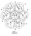
- each cell is represented as a hexagon; in practice, however, each cell has a shape that is dependent on, among other things, the topography of the terrain serviced by the system.
- Each cell includes a base station 12, which may be located approximately at its center.
- Each base station 12 is configured to transmit and receive signals within approximately the area defined by each cell 10.
- Dashed lines 18 in Fig. 2 illustrate the actual radio range of each base station. As illustrated, this actual radio range may extend beyond each cell area. Therefore, it is desired that a different set of frequencies be allocated to the adjacent cells to avoid interference.
- Subscribers located within each cell area communicate with other subscribers by using a wireless terminal 16 (e.g., a cellular telephone, a wireless local loop terminal, some cordless telephones, one-way and two-way pagers, PCS terminals and personal digital assistants).
- a wireless terminal 16 e.g., a cellular telephone, a wireless local loop terminal, some cordless telephones, one-way and two-way pagers, PCS terminals and personal digital assistants.
- Each wireless terminal located within a cell sends to and receives signals from the corresponding base station located in that cell, over a communications channel within a predetermined frequency range.
- the mean reuse distance D In order to increase the total number of channels available per unit area, it is desired to decrease the size of the cells. By reducing the size of the cells, it is possible to reuse the same frequency sets more often. Thus, more subscribers may be able to use the system, because of the increase of available frequency sets within a predetermined area. However, depending upon the size of each cell, the reuse distance D may become small enough to cause co-channel interference between the cells that use the same frequency range.
- One way to reduce the level of interference between cells that use the same frequency range is to employ directional antennas at each base station.
- Each cell is divided into several sectors, with each sector being served by a directional antenna located at the base station.
- By employing these directional antennas it is possible to allocate frequency sets to each sector such that the possibility of co-channel interference among cells employing these frequency sets is minimized.
- Each directional antenna may be used for both transmitting signals from the base station to the wireless terminal, or for receiving signals from the wireless terminals at the base station.
- each cell may be divided into a few sectors, for example three sectors, requiring a base station with three separate directional antennas. In more highly populated areas where the cells are substantially small, even higher number of sectors per cell may be desired so as to reduce co-channel interference.
- This sectorization technique is well-known and described in Cellular Radio Principles and Design , by Raymond C.V. Macario (McGraw Hill, 1993), which is incorporated herein by reference.
- One disadvantage of sectorization is the requirement of a more complex base station design. For example, when a wireless terminal is moving from one sector to another sector within the same cell, a technique may be employed to change the frequency with which the base and wireless terminals communicate. This change of communication frequency for an in process call is known as "hand-over" or "hand-off.” Although hand-off is required when traveling from one cell to the other, with sectorization, it may be also required when traveling from one sector to the other within the same cell.
- the sector-to-sector hand-off is particularly desired in frequency-division multiple access (“FDMA”) and time-division multiple access (“TDMA”) communication schemes.
- FDMA frequency-division multiple access
- TDMA time-division multiple access
- the operation of both of these communication schemes is well-known and described in Information Transmission, Modulation, And Noise , by Mischa Schwartz (3rd ed. McGraw Hill 1980), incorporated herein by reference.
- CDMA code-division multiple access
- TR 45 standard specification, entitled Mobile Station- Base Station Compatibility Standard for Dual-Mode Wideband Spread Spectrum Cellular System (to be published as IS-95-A) and incorporated herein by reference.
- CDMA code-division multiple access
- all wireless terminals within a cell transmit and receive signals over the same frequency channel and at the same time.
- Each wireless terminal uses a unique code to encode the user's information; at the base station, the received signal is decoded based on all the available unique codes.
- code-division multiple access is that a hand-off within one cell may not be necessary. Since all wireless terminals transmit signals over the same channel, it is not necessary to switch communication frequencies when traveling from one sector to another. However, the base station employing CDMA, still requires complex circuitry as will be explained in more detail hereinafter in reference with Fig. 3.
- an automatic gain control loop for a base station comprises a demodulator having at least one output terminal, the demodulator being adapted to demodulate signals received by the base station so as to provide a plurality of phase signals via its output terminals, the phase signals corresponding to the phase of the signals received by said base station; a plurality of variable-gain amplifiers are each adapted to receive one of the phase signals to change the amplitude of the phase signals; and a plurality of signal processing units each adapted so as to receive signals provided by the variable amplifiers, each of the signal processing units further adapted to generate a feedback control signal so as to control the gain of each one of the variable-gain amplifiers.
- a method for controlling the gain of signals received by a base station in a cellular communication system comprises the steps of: demodulating the signals so as to generate phase signals corresponding to the received signals; variably controlling the magnitude of each one of the phase signals based on a feedback control signal; and processing the phase signals so as to generate the feedback control signal.
- Fig. 1 illustrates a cell structure employed in wireless telecommunications systems such as the one used in connection with the present invention.
- Fig. 2 illustrates a block diagram of a base station for receiving signals from a sectorized cell in accordance with one embodiment of the present invention.
- Fig. 3 illustrates a block diagram of a prior art automatic gain control loop.
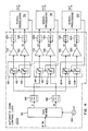
- Fig. 4 illustrates a block diagram of an automatic gain control loop for receiving signals from a sectorized cell in accordance with the present invention.
- Fig. 2 illustrates a block diagram of a base station 12 employed for receiving signals from wireless terminals located within a sectorized cell. It is assumed that this cell has been divided into three 120° sectors.
- Base station 12 may comprise three directional antennas, such as 210, 212 and 214 for receiving signals from a wireless terminal that may be located within one of the three sectors in a cell.
- the output of each antenna is coupled to an input terminal of a mixer, such as 216, 218 and 220, employed to convert the frequency range of the received signal from radio frequency RF to a lower intermediate frequency IF.
- the output terminal of each mixer is coupled to an automatic gain control loop, such as 222-i, 222-ii and 222-iii.
- Each gain control loop routes the incoming signal into three separate branches.
- Each branch is coupled to a signal processing unit, such as 76, 78 and 80, as will be explained in more detail.
- each one of the signal processing units receives three signals corresponding to antennas 210, 212 and 214 respectively, as illustrated in Fig. 2.
- Each signal processing unit may preferably generate three feedback signals, each of which is coupled to one of the automatic gain control loops 222.
- Fig. 2 illustrates: a feedback link from signal processing unit 76 to automatic gain control loop 222-i; a feedback link from signal processing 78 to automatic gain control loop 222-ii; and a feedback link from signal processing unit 80 to automatic gain control loop 222-iii.
- Base station 12 also includes: feedback links from signal processing unit 76 to automatic gain control loops 222-ii and 222-iii (not shown); feedback links from signal processing unit 78 to automatic gain control loops 222-i and 222-iii (not shown); and feedback links from signal processing unit 80 to automatic gain control loops 222-i and 222-ii (not shown).
- the magnitude of the voltage signals provided by each one of the automatic gain control loops is controlled by a feedback signal generated by each signal processing unit.
- the magnitude of the voltage signal provided by automatic gain control loop 222-i to signal processing unit 76 may be controlled by a feedback signal generated by signal processing unit 76.
- the magnitude of the voltage signal provided by automatic gain control loop 222-i, to signal processing unit 78 may be controlled by a feedback signal generated by signal processing unit 78.
- the magnitude of the voltage signal provided by automatic gain control loop 222-i, to signal processing unit 80 may be controlled by a feedback signal generated by signal processing unit 80.
- each automatic gain control loop may receive the same signal generated by a wireless terminal.
- Each automatic gain control loop provides the same signal to each one of the signal processing units.
- Each signal processing unit analyzes the signals received from each of the antennas. In response, it may control, for example, the signal generated by one of the automatic gain control loops.
- the output signal of each signal processing unit may be preferably coupled to a wireless switching center, which, in turn, may route this signal to a local switching office.
- FIG. 3 illustrates a block diagram of a prior art base station automatic gain control loop 222-a, typically employed for receiving signals from a sectorized cell. Again, it is assumed that this cell has been divided into three 120° sectors.
- Each antenna (not shown) may cover 1/3 of an entire cell.
- a wireless terminal transmits a signal to the base station. The base station may receive this signal through each one of the antennas.
- the output terminal of each antenna provides a signal that is coupled to an automatic gain control loop such as 222-a.
- the signals received by each antenna are fed to the input terminal of a 3-way divider 22 of a corresponding automatic gain control loop.
- the output terminals of the 3-way divider are coupled to the input terminal of three separate attenuators such as 28, 30, and 32.
- These attenuators may employ available designs such as diodes configured to function as a resistor.
- amplifiers with gains ranging from a negative value to a positive value may be employed. Therefore, in this discussion, attenuators and variable-gain amplifiers may be discussed interchangeably.
- each attenuator 28, 30 and 32 is respectively coupled to corresponding input terminals of demodulators 34, 36 and 38.
- Each demodulator provides a plurality of phase signals that correspond to the phase of the signals received by the modulator.
- demodulators 34, 36 and 38 may be a conventional QPSK demodulator like the one described in Information Transmission, Modulation, And Noise , by Mischa Schwartz (3rd ed. McGraw Hill 1980).
- Each demodulator 34, 36 and 38 includes two output terminals for providing in-phase ( I ) and quadri-phase ( Q ) component data signals. Each of these output terminals is in turn coupled to a low pass filter.
- Output terminals of demodulator 34 are respectively coupled to low pass filters 40 and 42.
- output terminals of demodulator 36 are respectively coupled to low pass filters 44 and 46.
- output terminals of demodulator 38 are respectively coupled to low pass filters 48 and 50. Each of these low pass filters substantially eliminates high frequency components of the received signals.
- each low pass filter is coupled to the input terminal of a signal amplifier such as operational amplifiers, 52, 54, 56, 58, 60 and 62.
- the output terminal of each of these amplifiers is coupled to the input terminal of an analog-to-digital (A/D) converter, such as converters 64, 66, 68, 70, 72 and 74.
- A/D analog-to-digital
- the output terminal of each analog-to-digital converter is, in turn, coupled to the input terminal of a signal processing unit, such as signal processing units 76, 78, and 80.
- Each signal processing unit provides data processing for each call in progress and certain administrative tasks.
- Signal processing unit determines the magnitude of signals received. It also generates a feedback control signal to adjust the gain of signals received by the base station antennas in an automatic gain control loop.
- Other functions of the signal processing unit include checking the identity of a wireless terminal whose signal is being processed, and checking whether the wireless terminal is within a satisfactory communications range.
- each signal processing unit is coupled to an input terminal of the corresponding attenuator contained in each automatic gain control loop.
- an output terminal of signal processing unit 76 is coupled to an input terminal of attenuator 28.
- An output terminal of signal processing unit 78 is coupled to an input terminal of attenuator 30.
- an output terminal of signal processing unit 80 is coupled to an input terminal of attenuator 32.
- Each signal processing unit is configured so as to provide a feedback signal to the corresponding attenuators 28, 30 and 32, in an automatic gain control loop, so as to control the attenuation of signals received by this automatic gain control loop.
- a local oscillator 26 generates a sinusoidal signal at its output terminal.
- the output signal from local oscillator 26 is coupled to each one of demodulators 34, 36 and 38 via a three-way divider 24.
- three way divider 24 utilizes the oscillating signal provided by local oscillator 26 to demodulate the signals received by the automatic gain control loop.
- some of the wireless terminals within a cell regardless of the sector within which they are located, transmit signals at the same frequency. Therefore, when a wireless terminal travels from one sector to the other, there may be no desire to switch communication channels.
- a wireless terminal sends a signal, which, depending on its location within the cell, is received by one or more of the antennas (not shown) located on base station 12.
- the output signal of each antenna is coupled to a corresponding automatic gain control loop, and in turn, its three way divider 22, which provides the same received signal through its three output terminals.
- the major components of an automatic gain control loop coupled to each antenna include three quadrature phase shift keying (QPSK) demodulators, three voltage variable attenuators, and two three-way dividers. These components require large board space and lead to substantially high manufacturing cost. The number of these components may be substantially reduced in accordance with one embodiment of the invention as explained hereinafter.
- QPSK quadrature phase shift keying
- Fig. 4 illustrates one embodiment of a base station automatic gain control loop, generally designated as 222-b, in accordance with the present invention, for receiving signals from a sectorized cell. Again, it is assumed that this cell has three 120° sectors. However, the invention is not limited in scope to a three-sector cell, and it will be clear to those skilled in the art how to make and use embodiments of the present invention that have a plurality of sectors. Typically, an automatic gain control loop in accordance with the present invention may be conveniently employed in a wireless telecommunications system wherein each cell may have several sectors.
- each antenna may serve 1/3 of an entire cell.
- a wireless terminal transmits a signal to a base station, such as one described in reference with Fig. 2.
- the base station may receive this signal through each one of the antennas.
- the output terminal of each antenna is coupled to an automatic gain control loop such as 222-b.
- the signal received by each antenna is fed to a corresponding input terminal of a quadrature phase shift keying demodulator 82.
- a local oscillator 84 provides an appropriate frequency signal to demodulator 82.
- this embodiment may employ QPSK demodulation, the present invention is not limited in scope in this respect and other modulation schemes may be employed.
- Demodulator 82 provides in-phase ( I ) and quadri-phase ( Q ) signal components through its two output terminals.
- the in-phase signal is preferably coupled to a low pass filter 86, and the quadri- phase signal is preferably coupled to a low pass filter 88.
- the output of low pass filter 86 may be coupled to one input terminal of three dual-mode voltage variable attenuators, such as 90, 96 and 104.
- the output terminal of low pass filter 88 may be coupled to the second input terminal of dual-mode voltage variable attenuators 90, 96 and 104.
- variable-gain amplifiers that are capable of both amplification and attenuation may also be used instead of the attenuators.
- Each dual-mode voltage variable attenuator 90, 96 and 104 advantageously comprises two voltage variable attenuators.
- dual-mode voltage variable attenuator 90 may include two voltage variable attenuators, such as 92 and 94.
- dual-mode voltage variable attenuator 96 may include two voltage variable attenuators, such as 98 and 102.
- dual-mode voltage variable attenuator 104 may include two voltage variable attenuators, such as 106 and 108.
- Voltage variable attenuator pairs 92 and 94, 98 and 102, 106 and 108 are preferably balanced so as to provide substantially equal amplification and phase delay in response to their respective input signals.
- a dual-mode variable-gain amplifier may be employed and configured to operate substantially the same as the dual, low noise, wideband variable-gain amplifier, model AD600/602 manufactured by Analog Devices, Norwood, MA.
- Such a dual-mode variable-gain amplifier contains two amplification channels, with each channel providing a variable-gain from -10 dB to +30 dB.
- a dual-mode variable attenuator may be configured to operate substantially the same as the balanced dual-mode variable attenuator, manufactured by Alpha Industries, Wooburn, MA.
- the amplitude of the in-phase and quadri-phase signal components of the received signal is variably controlled by a control voltage signal coupled to each dual-mode variable attenuator or amplifier.
- the output terminals of dual-mode variable attenuator 90 are preferably coupled to operational amplifiers 110 and 112, respectively.
- the output terminals of dual-mode variable attenuator 96 are preferably coupled to operational amplifiers 114 and 116, respectively.
- the output terminals of dual-mode variable attenuator 104 are preferably coupled to amplifiers 118 and 120, respectively.
- the output terminals of each of these amplifiers are coupled to an analog-to-digital (A/D) converter, such as 124, 126 and 128, 130 and 132, 134.
- A/D analog-to-digital converter
- the output terminals of analog-to-digital converters 124 and 126 are coupled to signal processing unit 76.
- the output terminals of analog-to-digital converters 128 and 130 are coupled to signal processing unit 78.
- the output terminals of analog-to-digital converters 132 and 134 are coupled to signal processing unit 80.
- each signal processing unit provides data processing for each call in progress and certain administrative tasks, such as those set forth in TR 45 standard specification, entitled Mobile Station- Base Station Compatibility Standard for Dual-Mode Wideband Spread Spectrum Cellular System (to be published as IS-95-A).
- Some functions of signal processing units include checking the identity of a wireless terminal whose signal is being processed, and whether the wireless terminal is within a satisfactory communications range.
- One output terminal of signal processing unit is coupled to an input terminal of the corresponding attenuator.
- an output terminal of signal processing unit 76 is coupled so as to provide a feedback control voltage signal to dual-mode variable attenuator 90.
- An output terminal of signal processing unit 78 is coupled so as to provide a feedback control voltage signal to dual-mode variable attenuator 96.
- an output terminal of signal processing unit 80 is coupled so as to provide a feedback control voltage signal to dual-mode variable attenuator 104.
- CDMA code-division multiple access
- a wireless terminal sends a signal, which, depending on its location within the cell, may be received by one or more of the antennas of the corresponding base station (not shown) located within a cell.
- the output signal of one of the antennas may be coupled to demodulator 82, via a mixer described in reference with Fig. 2, so as to demodulate the received signals.
- demodulator 82 For quadrature phase shift keying (QPSK) modulation, demodulator 82 provides in-phase and quadri-phase signals via two output terminals.
- QPSK quadrature phase shift keying
- the received signal may be demodulated into several phase signals.
- Low pass filters 86 and 88 may substantially eliminate high frequency component signals received from demodulator 82.
- Each in-phase and quadri-phase signal is preferably balanced by the dual-mode variable-gain attenuators such that the amplitude and phase delay of the in-phase and quadri-phase signals remain substantially equal.
- the output signals from the variable-gain attenuators are then preferably converted to a digital format by analog-to-digital converters and thereafter fed to the signal processing units.
- a feedback signal from each signal processing unit controls the attenuation of signals received by the dual-mode variable attenuators.
- the automatic gain control loop design for a wireless telecommunications base station in accordance with the present invention significantly reduces the required board space and manufacturing cost by eliminating demodulators and three-way power dividers.
Landscapes
- Mobile Radio Communication Systems (AREA)
- Control Of Amplification And Gain Control (AREA)
Applications Claiming Priority (2)
| Application Number | Priority Date | Filing Date | Title |
|---|---|---|---|
| US08/619,044 US5721757A (en) | 1996-03-20 | 1996-03-20 | Automatic gain control loop |
| US619044 | 1996-03-20 |
Publications (3)
| Publication Number | Publication Date |
|---|---|
| EP0797298A2 true EP0797298A2 (de) | 1997-09-24 |
| EP0797298A3 EP0797298A3 (de) | 1999-01-13 |
| EP0797298B1 EP0797298B1 (de) | 2003-07-23 |
Family
ID=24480226
Family Applications (1)
| Application Number | Title | Priority Date | Filing Date |
|---|---|---|---|
| EP97301679A Expired - Lifetime EP0797298B1 (de) | 1996-03-20 | 1997-03-12 | Automatische Verstärkungsregelschleife |
Country Status (5)
| Country | Link |
|---|---|
| US (1) | US5721757A (de) |
| EP (1) | EP0797298B1 (de) |
| JP (1) | JP3563225B2 (de) |
| CA (1) | CA2196240C (de) |
| DE (1) | DE69723606T2 (de) |
Cited By (8)
| Publication number | Priority date | Publication date | Assignee | Title |
|---|---|---|---|---|
| EP1166477A4 (de) * | 1999-03-01 | 2003-04-02 | Nokia Corp | Vorrichtung und verfahren zur selektiven veränderung von eigenschaften des empfangenen signals in einer empfängerstation |
| US6563891B1 (en) | 1998-11-24 | 2003-05-13 | Telefonaktiebolaget L M Ericsson (Publ) | Automatic gain control for slotted mode operation |
| GB2389251A (en) * | 2002-05-31 | 2003-12-03 | Hitachi Ltd | A polar-loop wireless communication apparatus, a semiconductor integrated circuit and a loop gain calibration method |
| EP1253714A3 (de) * | 2001-04-26 | 2004-03-17 | Zarlink Semiconductor Limited | Radiofrequenzschnittstelle |
| EP1309093A3 (de) * | 2001-10-31 | 2004-10-27 | Telefonaktiebolaget LM Ericsson (publ) | Verfahren und Vorrichtung zur Reduzierung von Schaltspitzen aufgrund von automatischen Verstärkungsumschaltungen |
| US7085544B2 (en) | 2002-05-31 | 2006-08-01 | Renesas Technology Corp. | Transmitter having a phase control loop whose frequency bandwidth is varied in accordance with modulation modes |
| US7209717B2 (en) | 2002-05-31 | 2007-04-24 | Renesas Technology Corporation | Apparatus for radio telecommunication system and method of building up output power |
| US7230997B2 (en) | 2002-05-31 | 2007-06-12 | Hitachi, Ltd. | Semiconductor integrated circuit for communication, radio-communications apparatus, and transmission starting method |
Families Citing this family (14)
| Publication number | Priority date | Publication date | Assignee | Title |
|---|---|---|---|---|
| ZA965340B (en) * | 1995-06-30 | 1997-01-27 | Interdigital Tech Corp | Code division multiple access (cdma) communication system |
| US7020111B2 (en) * | 1996-06-27 | 2006-03-28 | Interdigital Technology Corporation | System for using rapid acquisition spreading codes for spread-spectrum communications |
| US6900775B2 (en) | 1997-03-03 | 2005-05-31 | Celletra Ltd. | Active antenna array configuration and control for cellular communication systems |
| EP1012994A1 (de) * | 1997-03-03 | 2000-06-28 | Celletra Ltd. | Zellularkommunikationssystem |
| US20020051434A1 (en) * | 1997-10-23 | 2002-05-02 | Ozluturk Fatih M. | Method for using rapid acquisition spreading codes for spread-spectrum communications |
| JP3562967B2 (ja) * | 1998-08-06 | 2004-09-08 | アルプス電気株式会社 | Qpsk変調信号受信ユニット |
| WO2004095731A1 (ja) * | 2003-04-21 | 2004-11-04 | Sanyo Electric Co., Ltd. | 受信装置 |
| JP4050246B2 (ja) * | 2003-07-01 | 2008-02-20 | 松下電器産業株式会社 | 減衰器およびそれを用いた携帯電話端末装置 |
| EP1673197A1 (de) * | 2003-10-15 | 2006-06-28 | Duplomatic Automazione S.P.A. | Drehtisch mit eigener energiequelle zum montieren auf einer palette eines bearbeitungszentrums |
| JP3906209B2 (ja) * | 2004-01-26 | 2007-04-18 | 株式会社東芝 | 無線受信装置及び無線受信方法 |
| US7372925B2 (en) * | 2004-06-09 | 2008-05-13 | Theta Microelectronics, Inc. | Wireless LAN receiver with I and Q RF and baseband AGC loops and DC offset cancellation |
| US7978773B2 (en) | 2006-12-29 | 2011-07-12 | Agere Systems Inc. | Multi-channel receiver with improved AGC |
| US7769357B2 (en) * | 2007-04-25 | 2010-08-03 | Agere Systems Inc. | Multi-channel receiver with improved AGC |
| US7809343B2 (en) * | 2007-04-25 | 2010-10-05 | Agere Systems Inc. | Multi-channel receiver with improved AGC |
Family Cites Families (12)
| Publication number | Priority date | Publication date | Assignee | Title |
|---|---|---|---|---|
| FR2394218A1 (fr) * | 1977-06-10 | 1979-01-05 | Ibm France | Recepteur de donnees transmises par modulation binaire par saut de phase entrelacee |
| DE2909520C3 (de) * | 1979-03-10 | 1981-12-03 | Philips Patentverwaltung Gmbh, 2000 Hamburg | Schaltungsanordnung zur Dämpfung von Störgeräuschen |
| CA1278610C (en) * | 1987-09-21 | 1991-01-02 | Eisaku Sasaki | Stepped square-qam demodulator utilizing all signal points to generate control signals |
| US4894842A (en) * | 1987-10-15 | 1990-01-16 | The Charles Stark Draper Laboratory, Inc. | Precorrelation digital spread spectrum receiver |
| CH676179A5 (de) * | 1988-09-29 | 1990-12-14 | Ascom Zelcom Ag | |
| US4901332A (en) * | 1988-10-27 | 1990-02-13 | Unisys Corp. | Noncoherent-coherent A.C. coupled base band AGC receiver |
| US5095536A (en) * | 1990-03-23 | 1992-03-10 | Rockwell International Corporation | Direct conversion receiver with tri-phase architecture |
| US5321849A (en) * | 1991-05-22 | 1994-06-14 | Southwestern Bell Technology Resources, Inc. | System for controlling signal level at both ends of a transmission link based on a detected valve |
| JP2730347B2 (ja) * | 1991-10-09 | 1998-03-25 | 松下電器産業株式会社 | 受信機の自動利得制御方法 |
| JPH05211670A (ja) * | 1992-01-14 | 1993-08-20 | Nec Corp | 搬送波電力対雑音電力比検出回路 |
| JP2911773B2 (ja) * | 1994-03-18 | 1999-06-23 | 富士通株式会社 | ディジタル多重無線受信装置 |
| US5566201A (en) * | 1994-09-27 | 1996-10-15 | Nokia Mobile Phones Ltd. | Digital AGC for a CDMA radiotelephone |
-
1996
- 1996-03-20 US US08/619,044 patent/US5721757A/en not_active Expired - Lifetime
-
1997
- 1997-01-29 CA CA002196240A patent/CA2196240C/en not_active Expired - Fee Related
- 1997-03-11 JP JP05591497A patent/JP3563225B2/ja not_active Expired - Lifetime
- 1997-03-12 EP EP97301679A patent/EP0797298B1/de not_active Expired - Lifetime
- 1997-03-12 DE DE69723606T patent/DE69723606T2/de not_active Expired - Lifetime
Cited By (15)
| Publication number | Priority date | Publication date | Assignee | Title |
|---|---|---|---|---|
| US6563891B1 (en) | 1998-11-24 | 2003-05-13 | Telefonaktiebolaget L M Ericsson (Publ) | Automatic gain control for slotted mode operation |
| EP1166477A4 (de) * | 1999-03-01 | 2003-04-02 | Nokia Corp | Vorrichtung und verfahren zur selektiven veränderung von eigenschaften des empfangenen signals in einer empfängerstation |
| EP1253714A3 (de) * | 2001-04-26 | 2004-03-17 | Zarlink Semiconductor Limited | Radiofrequenzschnittstelle |
| US6963733B2 (en) | 2001-10-31 | 2005-11-08 | Telefonaktiebolaget L M Ericsson (Publ) | Method and apparatus for reducing the effect of AGC switching transients |
| EP1309093A3 (de) * | 2001-10-31 | 2004-10-27 | Telefonaktiebolaget LM Ericsson (publ) | Verfahren und Vorrichtung zur Reduzierung von Schaltspitzen aufgrund von automatischen Verstärkungsumschaltungen |
| GB2389251B (en) * | 2002-05-31 | 2005-09-07 | Hitachi Ltd | A communication semiconductor integrated circuit, a wireless communication apparatus, and a loop gain calibration method |
| GB2389251A (en) * | 2002-05-31 | 2003-12-03 | Hitachi Ltd | A polar-loop wireless communication apparatus, a semiconductor integrated circuit and a loop gain calibration method |
| US7082290B2 (en) | 2002-05-31 | 2006-07-25 | Renesas Technology Corp. | Communication semiconductor integrated circuit, a wireless communication apparatus, and a loop gain calibration method |
| US7085544B2 (en) | 2002-05-31 | 2006-08-01 | Renesas Technology Corp. | Transmitter having a phase control loop whose frequency bandwidth is varied in accordance with modulation modes |
| US7209717B2 (en) | 2002-05-31 | 2007-04-24 | Renesas Technology Corporation | Apparatus for radio telecommunication system and method of building up output power |
| US7230997B2 (en) | 2002-05-31 | 2007-06-12 | Hitachi, Ltd. | Semiconductor integrated circuit for communication, radio-communications apparatus, and transmission starting method |
| US7248842B2 (en) | 2002-05-31 | 2007-07-24 | Renesas Technology Corp. | Wireless communication apparatus having a phase control loop shared by first and second modulation modes and an amplitude control loop |
| US7366481B2 (en) | 2002-05-31 | 2008-04-29 | Renesas Technology Corporation | Apparatus for radio telecommunication system and method of building up output power |
| US7433653B2 (en) | 2002-05-31 | 2008-10-07 | Renesas Technology Corp. | Transmitter and semiconductor integrated circuit for communication |
| US7480345B2 (en) | 2002-05-31 | 2009-01-20 | Renesas Technology Corp. | Semiconductor integrated circuit for communication, radio-communication apparatus, and transmission starting method |
Also Published As
| Publication number | Publication date |
|---|---|
| EP0797298B1 (de) | 2003-07-23 |
| JPH1051251A (ja) | 1998-02-20 |
| CA2196240C (en) | 2000-09-05 |
| DE69723606D1 (de) | 2003-08-28 |
| JP3563225B2 (ja) | 2004-09-08 |
| EP0797298A3 (de) | 1999-01-13 |
| DE69723606T2 (de) | 2004-05-13 |
| CA2196240A1 (en) | 1997-09-21 |
| US5721757A (en) | 1998-02-24 |
Similar Documents
| Publication | Publication Date | Title |
|---|---|---|
| US5721757A (en) | Automatic gain control loop | |
| US5818827A (en) | Radio communication device and radio communication method | |
| US6130897A (en) | Time division multiple access FDD/TDD dual mode radio and a time division multiple access TDD dual band system | |
| EP0476569A2 (de) | Mobiles Kommunikationssystem | |
| US7395087B2 (en) | Radio receiver and signal amplifying method in radio receiver | |
| US6415153B1 (en) | System and method for aggregate overload control | |
| KR19990088052A (ko) | 다중반송파광대역시디엠에이시스템에서의전력제어를제공하는방법및장치 | |
| EP1178692A1 (de) | System und Verfahren zur Frequenzzuweisung in einem drahtlosen Kommunikationssystem | |
| JPH02190039A (ja) | 分散無線システムの回線接続方法 | |
| WO1993002519A1 (en) | Transition generating between on and off states of a radio frequency transmitter | |
| Suzuki et al. | Software radio base and personal station prototypes | |
| KR20040008750A (ko) | 이동통신 시스템에서의 적응 섹터 기술을 이용한 셀 용량증대 장치 및 그 제어 방법 | |
| AU718003B2 (en) | Method for controlling a base station, and a base station | |
| US5548799A (en) | Mobile communication system having a control for limiting the number of carriers based on the level of intermodulation distortion | |
| KR100266868B1 (ko) | 코드분할다중접속기지국시스템의파일럿송신기 | |
| JPH0795141A (ja) | 多チャンネル周波数多重信号パワーコントロール方式 | |
| KR100537081B1 (ko) | 통합 기지국 시스템의 무선 트래픽 부하 측정 장치 및 방법 | |
| KR100307704B1 (ko) | 이동통신시스템에서의셀그룹화동적제어장치및그방법 | |
| JPH07245539A (ja) | 自動利得制御回路 | |
| KR100267190B1 (ko) | 이동통신 기지국 하향주파수 변환기의 프론-엔드 장치 | |
| JP2001157271A (ja) | ある特定の信号強度をもつ信号を受信する装置とその方法 | |
| JPH06326652A (ja) | スペクトラム拡散移動通信の通信中チャネル切替方法 | |
| JPH03208433A (ja) | 無線電話受信機における自動利得制御回路 | |
| KR100222427B1 (ko) | 아날로그/ 코드분할 다중접속 방식 겸용 부스터 및 그 제어방법 | |
| KR100390399B1 (ko) | 이동통신시스템에서의비지/유휴비트송수신방법 |
Legal Events
| Date | Code | Title | Description |
|---|---|---|---|
| PUAI | Public reference made under article 153(3) epc to a published international application that has entered the european phase |
Free format text: ORIGINAL CODE: 0009012 |
|
| AK | Designated contracting states |
Kind code of ref document: A2 Designated state(s): DE FR GB |
|
| PUAL | Search report despatched |
Free format text: ORIGINAL CODE: 0009013 |
|
| AK | Designated contracting states |
Kind code of ref document: A3 Designated state(s): DE FR GB |
|
| 17P | Request for examination filed |
Effective date: 19990705 |
|
| GRAH | Despatch of communication of intention to grant a patent |
Free format text: ORIGINAL CODE: EPIDOS IGRA |
|
| GRAH | Despatch of communication of intention to grant a patent |
Free format text: ORIGINAL CODE: EPIDOS IGRA |
|
| GRAA | (expected) grant |
Free format text: ORIGINAL CODE: 0009210 |
|
| AK | Designated contracting states |
Designated state(s): DE FR GB |
|
| REG | Reference to a national code |
Ref country code: GB Ref legal event code: FG4D |
|
| REF | Corresponds to: |
Ref document number: 69723606 Country of ref document: DE Date of ref document: 20030828 Kind code of ref document: P |
|
| ET | Fr: translation filed | ||
| PLBE | No opposition filed within time limit |
Free format text: ORIGINAL CODE: 0009261 |
|
| STAA | Information on the status of an ep patent application or granted ep patent |
Free format text: STATUS: NO OPPOSITION FILED WITHIN TIME LIMIT |
|
| 26N | No opposition filed |
Effective date: 20040426 |
|
| PGFP | Annual fee paid to national office [announced via postgrant information from national office to epo] |
Ref country code: FR Payment date: 20140311 Year of fee payment: 18 |
|
| REG | Reference to a national code |
Ref country code: DE Ref legal event code: R082 Ref document number: 69723606 Country of ref document: DE Representative=s name: DILG HAEUSLER SCHINDELMANN PATENTANWALTSGESELL, DE |
|
| REG | Reference to a national code |
Ref country code: FR Ref legal event code: ST Effective date: 20151130 |
|
| PG25 | Lapsed in a contracting state [announced via postgrant information from national office to epo] |
Ref country code: FR Free format text: LAPSE BECAUSE OF NON-PAYMENT OF DUE FEES Effective date: 20150331 |
|
| PGFP | Annual fee paid to national office [announced via postgrant information from national office to epo] |
Ref country code: DE Payment date: 20160218 Year of fee payment: 20 |
|
| PGFP | Annual fee paid to national office [announced via postgrant information from national office to epo] |
Ref country code: GB Payment date: 20160223 Year of fee payment: 20 |
|
| REG | Reference to a national code |
Ref country code: DE Ref legal event code: R071 Ref document number: 69723606 Country of ref document: DE |
|
| REG | Reference to a national code |
Ref country code: GB Ref legal event code: PE20 Expiry date: 20170311 |
|
| PG25 | Lapsed in a contracting state [announced via postgrant information from national office to epo] |
Ref country code: GB Free format text: LAPSE BECAUSE OF EXPIRATION OF PROTECTION Effective date: 20170311 |