EP0797301A2 - Procédé pour le réglage de la mise en conduction d'un transistor bipolaire à grille isolée et dispositif pour sa mise en oeuvre - Google Patents
Procédé pour le réglage de la mise en conduction d'un transistor bipolaire à grille isolée et dispositif pour sa mise en oeuvre Download PDFInfo
- Publication number
- EP0797301A2 EP0797301A2 EP97810113A EP97810113A EP0797301A2 EP 0797301 A2 EP0797301 A2 EP 0797301A2 EP 97810113 A EP97810113 A EP 97810113A EP 97810113 A EP97810113 A EP 97810113A EP 0797301 A2 EP0797301 A2 EP 0797301A2
- Authority
- EP
- European Patent Office
- Prior art keywords
- voltage
- igbt
- gate
- function
- current
- Prior art date
- Legal status (The legal status is an assumption and is not a legal conclusion. Google has not performed a legal analysis and makes no representation as to the accuracy of the status listed.)
- Granted
Links
Images

Classifications
-
- H—ELECTRICITY
- H03—ELECTRONIC CIRCUITRY
- H03K—PULSE TECHNIQUE
- H03K17/00—Electronic switching or gating, i.e. not by contact-making and –breaking
- H03K17/51—Electronic switching or gating, i.e. not by contact-making and –breaking characterised by the components used
- H03K17/56—Electronic switching or gating, i.e. not by contact-making and –breaking characterised by the components used by the use, as active elements, of semiconductor devices
- H03K17/567—Circuits characterised by the use of more than one type of semiconductor device, e.g. BIMOS, composite devices such as IGBT
-
- H—ELECTRICITY
- H03—ELECTRONIC CIRCUITRY
- H03K—PULSE TECHNIQUE
- H03K17/00—Electronic switching or gating, i.e. not by contact-making and –breaking
- H03K17/08—Modifications for protecting switching circuit against overcurrent or overvoltage
- H03K17/081—Modifications for protecting switching circuit against overcurrent or overvoltage without feedback from the output circuit to the control circuit
- H03K17/0812—Modifications for protecting switching circuit against overcurrent or overvoltage without feedback from the output circuit to the control circuit by measures taken in the control circuit
- H03K17/08128—Modifications for protecting switching circuit against overcurrent or overvoltage without feedback from the output circuit to the control circuit by measures taken in the control circuit in composite switches
-
- H—ELECTRICITY
- H03—ELECTRONIC CIRCUITRY
- H03K—PULSE TECHNIQUE
- H03K17/00—Electronic switching or gating, i.e. not by contact-making and –breaking
- H03K17/16—Modifications for eliminating interference voltages or currents
- H03K17/161—Modifications for eliminating interference voltages or currents in field-effect transistor switches
- H03K17/162—Modifications for eliminating interference voltages or currents in field-effect transistor switches without feedback from the output circuit to the control circuit
- H03K17/163—Soft switching
-
- H—ELECTRICITY
- H03—ELECTRONIC CIRCUITRY
- H03K—PULSE TECHNIQUE
- H03K17/00—Electronic switching or gating, i.e. not by contact-making and –breaking
- H03K17/16—Modifications for eliminating interference voltages or currents
- H03K17/168—Modifications for eliminating interference voltages or currents in composite switches
Definitions
- the invention relates to the field of power electronics. It is based on a method for switching on the control of a bipolar transistor with an insulated gate electrode (IGBT) according to the preamble of the first claim. Furthermore, it relates to a device for performing the method.
- IGBT insulated gate electrode
- Such a device is part of a so-called gate drive.
- This is used to control the IGBT, ie it supplies the required switch-on and switch-off pulses.
- Another important task of the gate drive is to protect the IGBT from excessive voltages or currents in all operating states. This includes in particular a limitation of the current and voltage steepness. Limiting the rate of current rise also serves to protect the diode involved in the switching process.
- Known gate drives such as the one from the mentioned article "Optimization ofthe Short-Circuit " essentially consist of a voltage source, the two voltages, one for the switched-on state (typically 15V) and one for the switched-off state (typically 15V ) can deliver.
- This binary voltage source is connected to the IGBT gate through a resistor that limits the current into the gate.
- the gate which can be considered a capacitance, is loaded. The further the gate voltage has risen, the smaller the gate current and the slower the gate voltage rises.
- an attempt is made to record this on the load side, usually by measuring the voltage drop across an already existing parasitic inductance. With a suitable feedback current is usually drawn past the gate by opening a parallel path, which slows down the charging process.
- the disadvantage of this solution is that an additional load-side sensor is necessary. In addition, the signal obtained is small and therefore susceptible to interference.
- the loading of the oxide capacity of the IGBT when switching on is usually very slow because the current-driving difference across the gate resistor is small. The associated speed of the load-side voltage reduction is difficult to control and mostly too slow.
- the method is intended to allow the rate of current rise to be regulated when switched on (di / dt) without the current being detected on the load side.
- the essence of the invention is therefore that, in contrast to the prior art, it is not the gate voltage that is used as the control variable, but the gate current.
- This acts on the gate electrode in accordance with a target-actual comparison of an actual voltage value applied to the gate electrode and a corresponding target value.
- the regulation guides the load current during the switching process on a predetermined trajectory. Nevertheless, no current detection is necessary on the load side. Instead, one makes use of the fact that the behavior of the MOSFET in the IGBT dominates when the MOSFET is switched on. It can be shown (see below) that there is a quadratic relationship between the gate voltage and the load current as soon as the gate voltage increases than the threshold voltage is. This applies until the full load current flows. Controlling the gate voltage to a specific trajectory from the switched-off to the switched-on state causes the load current to increase quadratically in proportion to it. Conversely, the gate voltage curve for a desired load current curve can easily be calculated.
- the gate of the IGBT is an electrical capacitance on which the voltage must now be regulated.
- the control variable can only be the current into the gate.
- a simple proportional controller is sufficient as control.
- the gate current is then proportional to the difference between the desired and the actual gate voltage.
- a function generator is connected to a voltage-controlled current source via a comparator and a proportional controller. The function generator is controlled along a selected curve. The current source driven in this way impresses the desired control current into the gate of the IGBT.
- the invention In addition to completely mastering the current rise when switched on, the invention also brings advantages for the other operating states.
- the gate can be charged up to the threshold voltage very quickly, because this has no influence on the load side.
- the speed of the load-side voltage change at the IGBT can also be limited by limiting the gate current, because the oxide capacity is charged more slowly with a smaller gate current.
- the voltage rise when the IGBT is switched off can also be influenced by specifying suitable target voltage voltage profiles.
- the invention is based on a non-trivial, in-depth analysis of an IGBT model.
- An IGBT model is described, for example, in the article "An Experimentally Verfied IGBT Model Implemented in the Saber Circuit Simulator", IEEE Trans. On Power Electronics, Vol. 9, Sept. 1994, by A.R. Hefner and D.M. Diebolt described. This document also contains all of the equations used below.
- the MOS current is considered. According to FIG. 2, it is composed of two parts: the so-called emitter-base DC current ibp and a displacement current due to changes in base charge i ceb . Their sum is called i b .
- the current i b must be equal to the current from the drain D to the cathode 7 because of the node rule.
- This is also made up of three parts: the actual current in the MOS channel i mos , the current i mult , which reflects charge carrier multiplication by sudden ionization in a high electrical field, and the displacement current in the drain-source capacitance d (Q cdsj ) / German
- the current i mos is clearly determining.
- the current i b is thus practically equal to i mos .
- the load current when switching on is determined as the sum of the current in the MOS channel i mos and the proportion of the bipolar current determined by coupling the hole and electron transport (left summand in (1)) for the controller design. All other influences are interpreted as disturbances.
- MOS current imos and the bipolar current icp * add up to irb in the emitter node E (cf. FIG. 2) (equation (3)).
- i rb i cp * + i mos
- the total current is related to the MOS current according to equation (5).
- the two currents are therefore linearly proportional to one another.
- Inserting (6) in (5) gives a simple, quadratic relationship (7) between the load current and the gate voltage, which applies during the switch-on phase.
- Consequences for a regulation By controlling the gate voltage, the load current can be regulated during the rise. There is no need to measure the slope over the series true inductance in the load circuit.
- the control problem must now be put differently: The current into the gate of the IGBT serves as the control variable, while the gate voltage, which controls the IGBT, the size to be regulated.
- the regulation task to be solved is a so-called tracking task, in contrast to regulation on a working point. A suitable trajectory must now be found on which the controller has to guide. However, this also represents an additional degree of freedom for the circuit design.
- This controlled system represents an integrator, formed by the gate-source capacitance of the MOSFET and by the oxide capacitance. However, the oxide capacitance only has an influence at the end of the switch-on process.
- a proportional controller is a suitable controller. The resulting closed loop system is of the first order, so that no vibrations are possible. The gain of the proportional controller is limited by the maximum gate current available.
- Figure 1 shows an embodiment of such a control device.
- 1 designates the IGBT, to which a freewheeling diode 5 is antiparallel.
- These two elements can be part of a power electronic circuit such as of a multi-phase converter in a bridge circuit.
- a strongly inductive drive motor can be considered as the load of this circuit.
- the control electrode or gate electrode 6 of the IGBT 1 is fed by a voltage-controlled current source 2. This is arranged between the gate electrode 6 and the cathode electrode 7 of the IGBT 1.
- the controlling voltage is formed by the output voltage of a differential amplifier 4.
- the differential amplifier 4 forms a comparator and a proportional controller.
- a gate voltage is measured at the gate electrode 6 of the IGBT 1 and compared with a voltage trajectory specified by a function generator 3. The result of this setpoint / actual value comparison is amplified in the proportional controller and is used to control the current source 2.
- a current increase of approx. 0.8 kA / ⁇ s is to be achieved.
- the increase in voltage from -15 V (IGBT blocked) to the threshold voltage of e.g. 7 V can be freely selected since it has no influence on the load side.
- the maximum gate current that can be supplied by the current source has a limiting effect here.
- the voltage increase in this area can thus be linear in e.g. Rise 3 ⁇ s from -15 V to 7 V.
- the gate voltage for a 2.5kV IGBT must increase in 3 ⁇ s from 6.5V to 10.5V.
- the further increase up to the steady state voltage at 15V significantly influences the voltage drop rate of the IGBT.
- a straight line can also be used here, which is chosen to be steeper the steeper the voltage across the IGBT may drop. It is typically equally steep or slightly flatter than in the middle section, since in particular the gate voltage during the transition from the last to this section is dependent on the load current.
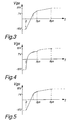
- the voltage trajectory thus forms three straight lines (FIG. 3).
- the first straight line rises from -15V to the threshold voltage.
- the second begins at the threshold voltage and rises to a gate voltage at which the IGBT is fully turned on.
- the third straight line then rises to 15V.
- Another variant is to combine the first two sections into an increase in shape
- This curve quickly leads the gate to the threshold voltage. In addition, it guides the load current in such a way that the rise in the lower area is steeper than in upper. This makes it possible to minimize the power loss while protecting the diode.
- the third section then also becomes one for the sake of simplicity Shape ( Figure 4).
- a course in the form of a root function is also conceivable in the middle section (FIG. 5). This variant is characterized in particular by minimizing the power loss proportional to the area under the current curve.
- the function generator for generating the voltage trajectories mentioned above can be constructed digitally or analog.
- the -Form on since this can be easily achieved by charging capacitors.
- the root form can also be realized, for example using a stored function table in the form of a look-up table.
- the invention thus provides a method for regulating the start-up of an IGBT and a corresponding device which achieves a current increase limitation in a circuit-technically simple manner without a current or voltage measurement on the load side.
Landscapes
- Power Conversion In General (AREA)
- Electronic Switches (AREA)
- Crystals, And After-Treatments Of Crystals (AREA)
- Die Bonding (AREA)
- Electrical Discharge Machining, Electrochemical Machining, And Combined Machining (AREA)
Applications Claiming Priority (2)
| Application Number | Priority Date | Filing Date | Title |
|---|---|---|---|
| DE19610895A DE19610895A1 (de) | 1996-03-20 | 1996-03-20 | Verfahren zur Einschaltregelung eines IGBTs und Vorrichtung zur Durchführung des Verfahrens |
| DE19610895 | 1996-03-20 |
Publications (3)
| Publication Number | Publication Date |
|---|---|
| EP0797301A2 true EP0797301A2 (fr) | 1997-09-24 |
| EP0797301A3 EP0797301A3 (fr) | 1999-06-02 |
| EP0797301B1 EP0797301B1 (fr) | 2001-08-22 |
Family
ID=7788819
Family Applications (1)
| Application Number | Title | Priority Date | Filing Date |
|---|---|---|---|
| EP97810113A Expired - Lifetime EP0797301B1 (fr) | 1996-03-20 | 1997-03-03 | Procédé pour le réglage de la mise en conduction d'un transistor bipolaire à grille isolée et dispositif pour sa mise en oeuvre |
Country Status (6)
| Country | Link |
|---|---|
| US (1) | US5877646A (fr) |
| EP (1) | EP0797301B1 (fr) |
| JP (1) | JPH1012629A (fr) |
| CN (1) | CN1132312C (fr) |
| AT (1) | ATE204684T1 (fr) |
| DE (2) | DE19610895A1 (fr) |
Cited By (5)
| Publication number | Priority date | Publication date | Assignee | Title |
|---|---|---|---|---|
| EP0996227A3 (fr) * | 1998-10-24 | 2001-03-28 | DaimlerChrysler AG | Procédé de contrôle de l'état de commutation d'un IGBT et dispositif pour la mise en oeuvre du procédé |
| EP1105970A4 (fr) * | 1998-06-12 | 2001-06-13 | South Island Discretes Ltd | Attaque de la grille pour semi-conducteurs de puissance a grille isolee |
| WO2002007315A1 (fr) * | 2000-07-13 | 2002-01-24 | Ct-Concept Technologie Ag | Procede et dispositif pour le reglage, en fonction de l'etat, du comportement transitoire de commutateurs a semi-conducteur de puissance |
| WO2013162794A1 (fr) * | 2012-04-24 | 2013-10-31 | General Electric Company | Appareil et procédé commutateur convertisseur |
| WO2013169423A1 (fr) * | 2012-05-11 | 2013-11-14 | General Electric Company | Procédé et appareil de commande d'un cycle thermique |
Families Citing this family (19)
| Publication number | Priority date | Publication date | Assignee | Title |
|---|---|---|---|---|
| DE10061563B4 (de) | 2000-12-06 | 2005-12-08 | RUBITEC Gesellschaft für Innovation und Technologie der Ruhr-Universität Bochum mbH | Verfahren und Vorrichtung zum Ein- und Ausschalten von Leistungshalbleitern, insbesondere für ein drehzahlvariables Betreiben einer Asynchronmaschine, ein Betreiben einer Zündschaltung für Ottomotoren, sowie Schaltnetzteil |
| US6552889B1 (en) * | 2001-07-17 | 2003-04-22 | Vishay Siliconix | Current limiting technique for hybrid power MOSFET circuits |
| DE10143432C1 (de) * | 2001-09-05 | 2003-02-27 | Daimler Chrysler Ag | Treiberschaltung und Ansteuerverfahren für einen feldgesteuerten Leistungsschalter |
| DE10355255A1 (de) * | 2003-11-26 | 2005-07-07 | Rexroth Indramat Gmbh | Verfahren zur Ansteuerung eines Bipolartransistors mit isolierter Gate-Elektrode und Vorrichtung zur Durchführung des Verfahrens |
| GB2417625A (en) * | 2004-08-31 | 2006-03-01 | Bombardier Transp Gmbh | Digital adaptive control of IGBT or MOS gate charging current in a converter for a railway traction motor |
| KR101913714B1 (ko) | 2012-04-20 | 2018-12-28 | 비쉐이-실리코닉스 | 전류 제한 시스템 및 방법 |
| DE102012207147B4 (de) | 2012-04-27 | 2016-01-21 | Infineon Technologies Ag | Verfahren zum Ansteuern von Leistungshalbleiterschaltern |
| US8836404B2 (en) | 2012-08-02 | 2014-09-16 | Vishay-Siliconix | Circuit for preventing reverse conduction |
| US9356515B2 (en) | 2012-09-14 | 2016-05-31 | Freescale Semiconductor, Inc. | Power switching device, three phase bridge inverter, and method of operating a power switching device |
| JP6504832B2 (ja) | 2014-01-28 | 2019-04-24 | ゼネラル・エレクトリック・カンパニイ | 統合された取り付けおよび冷却の装置、電子装置、および車両 |
| EP3219010B1 (fr) * | 2014-11-11 | 2020-07-08 | Maschinenfabrik Reinhausen GmbH | Émulation de résistance et amplificateur de grille |
| GB2532214A (en) * | 2014-11-11 | 2016-05-18 | Reinhausen Maschf Scheubeck | Resistor emulation |
| US9425786B2 (en) | 2014-11-17 | 2016-08-23 | General Electric Company | System and method for driving a power switch |
| US10073512B2 (en) | 2014-11-19 | 2018-09-11 | General Electric Company | System and method for full range control of dual active bridge |
| CN105045961B (zh) * | 2015-06-24 | 2018-09-25 | 中国人民解放军海军工程大学 | 功率二极管短时续流反向恢复尖峰电压建模方法 |
| CN106301265B (zh) * | 2016-09-06 | 2018-10-23 | 安徽中研电气有限责任公司 | 一种igbt输出级的大功率运算放大器 |
| FR3056859B1 (fr) * | 2016-09-23 | 2018-11-30 | Alstom Transport Technologies | Procede de pilotage d'un transistor du type igbt et dispositif de pilotage associe |
| DE102016226147A1 (de) | 2016-12-23 | 2018-06-28 | Robert Bosch Gmbh | Vorrichtung und Vorrichtung zum Betreiben einer Leistungsendstufe |
| CN106991221B (zh) * | 2017-03-24 | 2020-04-24 | 清华大学 | 一种基于igbt器件瞬态物理过程的分段折线建模方法 |
Family Cites Families (10)
| Publication number | Priority date | Publication date | Assignee | Title |
|---|---|---|---|---|
| JPS6395727A (ja) * | 1986-10-13 | 1988-04-26 | Fuji Electric Co Ltd | Igbtのゲ−ト駆動回路 |
| DE3723786A1 (de) * | 1987-07-16 | 1989-01-26 | Licentia Gmbh | Anordnung zur selbsttaetigen ueberstromabschaltung |
| FR2663175A1 (fr) * | 1990-06-12 | 1991-12-13 | Merlin Gerin | Commutateur statique. |
| DE4034845A1 (de) * | 1990-11-02 | 1992-05-07 | Bayerische Motoren Werke Ag | Schaltanordnung in kraftfahrzeugen zum getakteten einschalten von induktiven verbrauchern |
| JP2674355B2 (ja) * | 1991-05-15 | 1997-11-12 | 三菱電機株式会社 | パワー素子の過電流保護装置 |
| JPH05327440A (ja) * | 1992-05-19 | 1993-12-10 | Fuji Electric Co Ltd | 駆動装置 |
| FR2700647B1 (fr) * | 1993-01-15 | 1995-03-31 | Legrand Sa | Commutateur statique à protection intégrée pour le couplage d'une charge à une source électrique, comportant un transistor bipolaire à grille isolée. |
| JPH07226663A (ja) * | 1994-02-10 | 1995-08-22 | Mitsubishi Electric Corp | トランジスタ駆動回路 |
| JP3123349B2 (ja) * | 1994-06-29 | 2001-01-09 | 富士電機株式会社 | 半導体装置の制御回路 |
| JP3442149B2 (ja) * | 1994-07-28 | 2003-09-02 | 富士通株式会社 | 半導体回路 |
-
1996
- 1996-03-20 DE DE19610895A patent/DE19610895A1/de not_active Withdrawn
-
1997
- 1997-01-31 US US08/792,232 patent/US5877646A/en not_active Expired - Fee Related
- 1997-03-03 EP EP97810113A patent/EP0797301B1/fr not_active Expired - Lifetime
- 1997-03-03 AT AT97810113T patent/ATE204684T1/de not_active IP Right Cessation
- 1997-03-03 DE DE59704344T patent/DE59704344D1/de not_active Expired - Lifetime
- 1997-03-17 JP JP9062636A patent/JPH1012629A/ja active Pending
- 1997-03-20 CN CN97103343A patent/CN1132312C/zh not_active Expired - Fee Related
Cited By (7)
| Publication number | Priority date | Publication date | Assignee | Title |
|---|---|---|---|---|
| EP1105970A4 (fr) * | 1998-06-12 | 2001-06-13 | South Island Discretes Ltd | Attaque de la grille pour semi-conducteurs de puissance a grille isolee |
| EP0996227A3 (fr) * | 1998-10-24 | 2001-03-28 | DaimlerChrysler AG | Procédé de contrôle de l'état de commutation d'un IGBT et dispositif pour la mise en oeuvre du procédé |
| WO2002007315A1 (fr) * | 2000-07-13 | 2002-01-24 | Ct-Concept Technologie Ag | Procede et dispositif pour le reglage, en fonction de l'etat, du comportement transitoire de commutateurs a semi-conducteur de puissance |
| WO2013162794A1 (fr) * | 2012-04-24 | 2013-10-31 | General Electric Company | Appareil et procédé commutateur convertisseur |
| US8717069B2 (en) | 2012-04-24 | 2014-05-06 | General Electric Company | Converter switch apparatus and method |
| WO2013169423A1 (fr) * | 2012-05-11 | 2013-11-14 | General Electric Company | Procédé et appareil de commande d'un cycle thermique |
| US8923022B2 (en) | 2012-05-11 | 2014-12-30 | General Electric Company | Method and apparatus for controlling thermal cycling |
Also Published As
| Publication number | Publication date |
|---|---|
| EP0797301A3 (fr) | 1999-06-02 |
| US5877646A (en) | 1999-03-02 |
| EP0797301B1 (fr) | 2001-08-22 |
| ATE204684T1 (de) | 2001-09-15 |
| CN1132312C (zh) | 2003-12-24 |
| JPH1012629A (ja) | 1998-01-16 |
| DE59704344D1 (de) | 2001-09-27 |
| CN1164145A (zh) | 1997-11-05 |
| DE19610895A1 (de) | 1997-09-25 |
Similar Documents
| Publication | Publication Date | Title |
|---|---|---|
| EP0797301B1 (fr) | Procédé pour le réglage de la mise en conduction d'un transistor bipolaire à grille isolée et dispositif pour sa mise en oeuvre | |
| DE102012207147B4 (de) | Verfahren zum Ansteuern von Leistungshalbleiterschaltern | |
| DE102012015787B3 (de) | Gepulster Gate-Treiber | |
| DE112007000857B4 (de) | Drei Treiberschaltungen für Halbleiterelemente mit Kurzschlusserfassung | |
| DE10061563B4 (de) | Verfahren und Vorrichtung zum Ein- und Ausschalten von Leistungshalbleitern, insbesondere für ein drehzahlvariables Betreiben einer Asynchronmaschine, ein Betreiben einer Zündschaltung für Ottomotoren, sowie Schaltnetzteil | |
| DE102005045099B4 (de) | Entsättigungsschaltung mit einem IGBT | |
| EP2608399B1 (fr) | Procédé de détection de défaut de terre pendant l'opération d'un convertisseur | |
| DE3432225A1 (de) | Rueckwaertsphasensteuerungsleistungsschaltkreis und leitungswinkelsteuerverfahren | |
| EP2638623B1 (fr) | Procédé de commande de deux igbt montés électriquement en série à conduction inverse d'un demi-pont | |
| EP2412096A2 (fr) | Dispositif de commutation pourvu d'un circuit en cascade | |
| DE10351843B4 (de) | Verfahren und elektrische Schaltungen zur Ermittlung einer Temperatur eines Leistungshalbleiters | |
| DE60313733T2 (de) | Ansteuerschaltung für einen Steueranschluss eines Bipolartransistors, der in der Emitterschattkonfiguration ist und entsprechenes Ansteuerverfahren | |
| EP0756782B1 (fr) | Circuit de commande a courant continu | |
| DE3514699A1 (de) | Integrierbare schaltungsanordnung zum steuern der abschaltspannungsaenderungsgeschwindigkeit von nichtgenerativen spannungsgesteuerten halbleiterschaltern | |
| DE2906961C2 (de) | Schaltungsanordnung mit einem feldgesteuerten Thyristor | |
| DE3420003A1 (de) | Anordnung zum verhindern uebermaessiger verlustleistung in einer leistungsschalthalbleitervorrichtung | |
| EP0854574B1 (fr) | Circuit d'attaque | |
| DE19527736C1 (de) | Schaltungsanordnung zur Ansteuerung eines dem Speisekreis einer elektrischen Last zugeordneten MOS-Feldeffekttransistors | |
| EP0314013B1 (fr) | Procédé de régulation du courant de base d'un transistor de commutation, et montage pour la réalisation du procédé | |
| EP3317967B1 (fr) | Circuit de commutation destiné à la commande d'un transistor | |
| DE102013015723B3 (de) | Verbesserte Ansteuerung von Leistungshalbleitern | |
| DE102016210798B3 (de) | Leistungshalbleiterschaltung | |
| DE19726765C2 (de) | Gatespannungsbegrenzung für eine Schaltungsanordnung | |
| EP0141427B1 (fr) | Modulateur d'impulsions de grille pour un tube à ondes progressives de haute puissance équipé d'une grille de commande | |
| DE102023200167A1 (de) | Schaltungsmodul und Halbleiterschalter mit einer Mehrzahl von in Reihe geschalteten Schaltungsmodulen |
Legal Events
| Date | Code | Title | Description |
|---|---|---|---|
| PUAI | Public reference made under article 153(3) epc to a published international application that has entered the european phase |
Free format text: ORIGINAL CODE: 0009012 |
|
| AK | Designated contracting states |
Kind code of ref document: A2 Designated state(s): AT CH DE ES FI FR GB IT LI SE |
|
| PUAL | Search report despatched |
Free format text: ORIGINAL CODE: 0009013 |
|
| AK | Designated contracting states |
Kind code of ref document: A3 Designated state(s): AT CH DE ES FI FR GB IT LI SE |
|
| 17P | Request for examination filed |
Effective date: 19991013 |
|
| 17Q | First examination report despatched |
Effective date: 20000504 |
|
| GRAG | Despatch of communication of intention to grant |
Free format text: ORIGINAL CODE: EPIDOS AGRA |
|
| GRAG | Despatch of communication of intention to grant |
Free format text: ORIGINAL CODE: EPIDOS AGRA |
|
| GRAH | Despatch of communication of intention to grant a patent |
Free format text: ORIGINAL CODE: EPIDOS IGRA |
|
| GRAH | Despatch of communication of intention to grant a patent |
Free format text: ORIGINAL CODE: EPIDOS IGRA |
|
| GRAA | (expected) grant |
Free format text: ORIGINAL CODE: 0009210 |
|
| AK | Designated contracting states |
Kind code of ref document: B1 Designated state(s): AT CH DE ES FI FR GB IT LI SE |
|
| PG25 | Lapsed in a contracting state [announced via postgrant information from national office to epo] |
Ref country code: IT Free format text: LAPSE BECAUSE OF FAILURE TO SUBMIT A TRANSLATION OF THE DESCRIPTION OR TO PAY THE FEE WITHIN THE PRE;WARNING: LAPSES OF ITALIAN PATENTS WITH EFFECTIVE DATE BEFORE 2007 MAY HAVE OCCURRED AT ANY TIME BEFORE 2007. THE CORRECT EFFECTIVE DATE MAY BE DIFFERENT FROM THE ONE RECORDED.SCRIBED TIME-LIMIT Effective date: 20010822 Ref country code: GB Free format text: LAPSE BECAUSE OF FAILURE TO SUBMIT A TRANSLATION OF THE DESCRIPTION OR TO PAY THE FEE WITHIN THE PRESCRIBED TIME-LIMIT Effective date: 20010822 Ref country code: FI Free format text: LAPSE BECAUSE OF FAILURE TO SUBMIT A TRANSLATION OF THE DESCRIPTION OR TO PAY THE FEE WITHIN THE PRESCRIBED TIME-LIMIT Effective date: 20010822 |
|
| REF | Corresponds to: |
Ref document number: 204684 Country of ref document: AT Date of ref document: 20010915 Kind code of ref document: T |
|
| REG | Reference to a national code |
Ref country code: CH Ref legal event code: EP |
|
| RAP2 | Party data changed (patent owner data changed or rights of a patent transferred) |
Owner name: BOMBARDIER TRANSPORTATION GMBH |
|
| REF | Corresponds to: |
Ref document number: 59704344 Country of ref document: DE Date of ref document: 20010927 |
|
| PG25 | Lapsed in a contracting state [announced via postgrant information from national office to epo] |
Ref country code: SE Free format text: LAPSE BECAUSE OF FAILURE TO SUBMIT A TRANSLATION OF THE DESCRIPTION OR TO PAY THE FEE WITHIN THE PRESCRIBED TIME-LIMIT Effective date: 20011122 |
|
| ET | Fr: translation filed | ||
| GBV | Gb: ep patent (uk) treated as always having been void in accordance with gb section 77(7)/1977 [no translation filed] |
Effective date: 20010822 |
|
| PG25 | Lapsed in a contracting state [announced via postgrant information from national office to epo] |
Ref country code: ES Free format text: LAPSE BECAUSE OF FAILURE TO SUBMIT A TRANSLATION OF THE DESCRIPTION OR TO PAY THE FEE WITHIN THE PRESCRIBED TIME-LIMIT Effective date: 20020228 |
|
| PG25 | Lapsed in a contracting state [announced via postgrant information from national office to epo] |
Ref country code: AT Free format text: LAPSE BECAUSE OF NON-PAYMENT OF DUE FEES Effective date: 20020303 |
|
| PG25 | Lapsed in a contracting state [announced via postgrant information from national office to epo] |
Ref country code: LI Free format text: LAPSE BECAUSE OF NON-PAYMENT OF DUE FEES Effective date: 20020331 Ref country code: CH Free format text: LAPSE BECAUSE OF NON-PAYMENT OF DUE FEES Effective date: 20020331 |
|
| PLBE | No opposition filed within time limit |
Free format text: ORIGINAL CODE: 0009261 |
|
| STAA | Information on the status of an ep patent application or granted ep patent |
Free format text: STATUS: NO OPPOSITION FILED WITHIN TIME LIMIT |
|
| 26N | No opposition filed | ||
| REG | Reference to a national code |
Ref country code: CH Ref legal event code: PL |
|
| PGFP | Annual fee paid to national office [announced via postgrant information from national office to epo] |
Ref country code: FR Payment date: 20130408 Year of fee payment: 17 Ref country code: DE Payment date: 20130321 Year of fee payment: 17 |
|
| REG | Reference to a national code |
Ref country code: DE Ref legal event code: R119 Ref document number: 59704344 Country of ref document: DE |
|
| REG | Reference to a national code |
Ref country code: FR Ref legal event code: ST Effective date: 20141128 |
|
| REG | Reference to a national code |
Ref country code: DE Ref legal event code: R119 Ref document number: 59704344 Country of ref document: DE Effective date: 20141001 |
|
| PG25 | Lapsed in a contracting state [announced via postgrant information from national office to epo] |
Ref country code: DE Free format text: LAPSE BECAUSE OF NON-PAYMENT OF DUE FEES Effective date: 20141001 Ref country code: FR Free format text: LAPSE BECAUSE OF NON-PAYMENT OF DUE FEES Effective date: 20140331 |