EP0798598A2 - Verfahren zur Behandlung eines Photoresists auf einem Substrat und Einrichtung dafür - Google Patents
Verfahren zur Behandlung eines Photoresists auf einem Substrat und Einrichtung dafür Download PDFInfo
- Publication number
- EP0798598A2 EP0798598A2 EP97105041A EP97105041A EP0798598A2 EP 0798598 A2 EP0798598 A2 EP 0798598A2 EP 97105041 A EP97105041 A EP 97105041A EP 97105041 A EP97105041 A EP 97105041A EP 0798598 A2 EP0798598 A2 EP 0798598A2
- Authority
- EP
- European Patent Office
- Prior art keywords
- processing
- resist
- concentration
- alkaline component
- processing region
- Prior art date
- Legal status (The legal status is an assumption and is not a legal conclusion. Google has not performed a legal analysis and makes no representation as to the accuracy of the status listed.)
- Withdrawn
Links
Images




Classifications
-
- H—ELECTRICITY
- H10—SEMICONDUCTOR DEVICES; ELECTRIC SOLID-STATE DEVICES NOT OTHERWISE PROVIDED FOR
- H10P—GENERIC PROCESSES OR APPARATUS FOR THE MANUFACTURE OR TREATMENT OF DEVICES COVERED BY CLASS H10
- H10P76/00—Manufacture or treatment of masks on semiconductor bodies, e.g. by lithography or photolithography
-
- H—ELECTRICITY
- H10—SEMICONDUCTOR DEVICES; ELECTRIC SOLID-STATE DEVICES NOT OTHERWISE PROVIDED FOR
- H10P—GENERIC PROCESSES OR APPARATUS FOR THE MANUFACTURE OR TREATMENT OF DEVICES COVERED BY CLASS H10
- H10P72/00—Handling or holding of wafers, substrates or devices during manufacture or treatment thereof
- H10P72/04—Apparatus for manufacture or treatment
- H10P72/0451—Apparatus for manufacturing or treating in a plurality of work-stations
- H10P72/0452—Apparatus for manufacturing or treating in a plurality of work-stations characterised by the layout of the process chambers
- H10P72/0456—Apparatus for manufacturing or treating in a plurality of work-stations characterised by the layout of the process chambers in-line arrangement
-
- G—PHYSICS
- G03—PHOTOGRAPHY; CINEMATOGRAPHY; ANALOGOUS TECHNIQUES USING WAVES OTHER THAN OPTICAL WAVES; ELECTROGRAPHY; HOLOGRAPHY
- G03F—PHOTOMECHANICAL PRODUCTION OF TEXTURED OR PATTERNED SURFACES, e.g. FOR PRINTING, FOR PROCESSING OF SEMICONDUCTOR DEVICES; MATERIALS THEREFOR; ORIGINALS THEREFOR; APPARATUS SPECIALLY ADAPTED THEREFOR
- G03F7/00—Photomechanical, e.g. photolithographic, production of textured or patterned surfaces, e.g. printing surfaces; Materials therefor, e.g. comprising photoresists; Apparatus specially adapted therefor
- G03F7/16—Coating processes; Apparatus therefor
-
- G—PHYSICS
- G03—PHOTOGRAPHY; CINEMATOGRAPHY; ANALOGOUS TECHNIQUES USING WAVES OTHER THAN OPTICAL WAVES; ELECTROGRAPHY; HOLOGRAPHY
- G03F—PHOTOMECHANICAL PRODUCTION OF TEXTURED OR PATTERNED SURFACES, e.g. FOR PRINTING, FOR PROCESSING OF SEMICONDUCTOR DEVICES; MATERIALS THEREFOR; ORIGINALS THEREFOR; APPARATUS SPECIALLY ADAPTED THEREFOR
- G03F7/00—Photomechanical, e.g. photolithographic, production of textured or patterned surfaces, e.g. printing surfaces; Materials therefor, e.g. comprising photoresists; Apparatus specially adapted therefor
- G03F7/26—Processing photosensitive materials; Apparatus therefor
-
- G—PHYSICS
- G03—PHOTOGRAPHY; CINEMATOGRAPHY; ANALOGOUS TECHNIQUES USING WAVES OTHER THAN OPTICAL WAVES; ELECTROGRAPHY; HOLOGRAPHY
- G03F—PHOTOMECHANICAL PRODUCTION OF TEXTURED OR PATTERNED SURFACES, e.g. FOR PRINTING, FOR PROCESSING OF SEMICONDUCTOR DEVICES; MATERIALS THEREFOR; ORIGINALS THEREFOR; APPARATUS SPECIALLY ADAPTED THEREFOR
- G03F7/00—Photomechanical, e.g. photolithographic, production of textured or patterned surfaces, e.g. printing surfaces; Materials therefor, e.g. comprising photoresists; Apparatus specially adapted therefor
- G03F7/70—Microphotolithographic exposure; Apparatus therefor
- G03F7/70691—Handling of masks or workpieces
- G03F7/70733—Handling masks and workpieces, e.g. exchange of workpiece or mask, transport of workpiece or mask
- G03F7/7075—Handling workpieces outside exposure position, e.g. SMIF box
-
- G—PHYSICS
- G03—PHOTOGRAPHY; CINEMATOGRAPHY; ANALOGOUS TECHNIQUES USING WAVES OTHER THAN OPTICAL WAVES; ELECTROGRAPHY; HOLOGRAPHY
- G03F—PHOTOMECHANICAL PRODUCTION OF TEXTURED OR PATTERNED SURFACES, e.g. FOR PRINTING, FOR PROCESSING OF SEMICONDUCTOR DEVICES; MATERIALS THEREFOR; ORIGINALS THEREFOR; APPARATUS SPECIALLY ADAPTED THEREFOR
- G03F7/00—Photomechanical, e.g. photolithographic, production of textured or patterned surfaces, e.g. printing surfaces; Materials therefor, e.g. comprising photoresists; Apparatus specially adapted therefor
- G03F7/70—Microphotolithographic exposure; Apparatus therefor
- G03F7/708—Construction of apparatus, e.g. environment aspects, hygiene aspects or materials
- G03F7/70858—Environment aspects, e.g. pressure of beam-path gas, temperature
- G03F7/70866—Environment aspects, e.g. pressure of beam-path gas, temperature of mask or workpiece
-
- H—ELECTRICITY
- H10—SEMICONDUCTOR DEVICES; ELECTRIC SOLID-STATE DEVICES NOT OTHERWISE PROVIDED FOR
- H10P—GENERIC PROCESSES OR APPARATUS FOR THE MANUFACTURE OR TREATMENT OF DEVICES COVERED BY CLASS H10
- H10P72/00—Handling or holding of wafers, substrates or devices during manufacture or treatment thereof
- H10P72/04—Apparatus for manufacture or treatment
- H10P72/0402—Apparatus for fluid treatment
-
- H—ELECTRICITY
- H10—SEMICONDUCTOR DEVICES; ELECTRIC SOLID-STATE DEVICES NOT OTHERWISE PROVIDED FOR
- H10P—GENERIC PROCESSES OR APPARATUS FOR THE MANUFACTURE OR TREATMENT OF DEVICES COVERED BY CLASS H10
- H10P72/00—Handling or holding of wafers, substrates or devices during manufacture or treatment thereof
- H10P72/04—Apparatus for manufacture or treatment
- H10P72/0451—Apparatus for manufacturing or treating in a plurality of work-stations
- H10P72/0452—Apparatus for manufacturing or treating in a plurality of work-stations characterised by the layout of the process chambers
- H10P72/0458—Apparatus for manufacturing or treating in a plurality of work-stations characterised by the layout of the process chambers vertical arrangement
-
- Y—GENERAL TAGGING OF NEW TECHNOLOGICAL DEVELOPMENTS; GENERAL TAGGING OF CROSS-SECTIONAL TECHNOLOGIES SPANNING OVER SEVERAL SECTIONS OF THE IPC; TECHNICAL SUBJECTS COVERED BY FORMER USPC CROSS-REFERENCE ART COLLECTIONS [XRACs] AND DIGESTS
- Y10—TECHNICAL SUBJECTS COVERED BY FORMER USPC
- Y10S—TECHNICAL SUBJECTS COVERED BY FORMER USPC CROSS-REFERENCE ART COLLECTIONS [XRACs] AND DIGESTS
- Y10S414/00—Material or article handling
- Y10S414/135—Associated with semiconductor wafer handling
Definitions
- the present invention relates to a method of processing a resist onto a substrate such that a photoresist is coated with a substrate such as a semiconductor wafer and then the coated photoresist is exposed and developed, and to a resist processing apparatus.
- the chemically amplified resist is exposed to light, acid generated from the sensitive material is diffused due to heating process to act on a catalyst, thus causing base resin to be decomposed or causing the molecular structure of the base resin to be changed. It leads to a fact that the base resin is made to be soluble or insoluble with respect to the developer.
- the chemically amplified resist Since one molecule of the catalyst of the chemically amplified resist contributes to a plurality of chemical reactions, higher photosensitivity is realized as compared with conventional resists. Moreover, the chemically amplified resist, having a high light transmittance in a short wavelength region, is able to relax the light intensity distribution in the direction of the thickness of the film even if eximer laser beam having a short exposing wavelength is used. Thus, line widths of a level of 0.3 mm can be realized when a circuit pattern is formed.
- the chemically amplified resist depending on the environment by a degree greater than the conventional resists, has a risk that organic amine, such as ammonia and NMP (N-methyl.2 pyrrolidinone), and their polar materials (hereinafter simply called as "alkaline components"), each existing in the processing atmosphere in a small quantity, and the chemically amplified resist cause neutralization reactions to take place and thus the resist is devitalized. If the resist is devitalized, accurate line widths of a highly-integrated circuit pattern cannot be realized in the developing process. Thus, a so-called defective resolution takes place.
- organic amine such as ammonia and NMP (N-methyl.2 pyrrolidinone)
- alkaline components N-methyl.2 pyrrolidinone
- the inventors of the present invention have developed and researched the foregoing problem, thus resulting in consideration being performed such that the following three facts relate to the alkaline component which is mixed in the processing atmosphere.
- a solution containing ammonia as washing liquid for removing particles allowed to adhere to non-processed wafer causes alkaline component to be generated in the processing atmosphere.
- a second fact is such that use of hexamethyldisilazane (HMDS) in the adhesion process which is performed before the resist is applied causes the alkaline component to be generated in the processing atmosphere.
- HMDS hexamethyldisilazane
- a third fact is that a process for forming a reflection preventive film on the surface of the wafer by using amine solvent results in the alkaline component being generated in the processing atmosphere.
- a resist processing apparatus which comprises a special chemical filter capable of removing alkaline component in the resist processing atmosphere.
- the element of the chemical filter is impregnated with acid components, such as phosphoric acid, so as to remove the alkaline component attributable to the neutralizing reaction with the acid component so that clean downflow air is introduced into a processing portion. If the foregoing apparatus is used for a long time and thus the filter element deteriorates causing the removal performance also deteriorates, the filter element must be changed at proper timing because the concentration of the alkaline component in the processing atmosphere is raised gradually.
- An object of the present invention is to provide a method of processing a resist onto a substrate and a resist processing apparatus capable of raising manufacturing yield of semiconductor devices having a highly-integrated circuit pattern and improving the reliability of the apparatus.
- a method of processing a resist onto a substrate such that the substrate is subjected to a resist process in a resist processing system having a processing region and a non-processing region which are air-conditioned, the method of processing a resist onto a substrate comprising:
- a method of processing a resist onto a substrate such that the substrate is subjected to a resist process in a resist processing system having a processing region and a non-processing region which are air-conditioned, the method of processing a resist onto a substrate comprising:
- a resist processing apparatus having a processing region and a non-processing region which are air-conditioned, the resist processing apparatus comprising:
- a resist processing apparatus having a processing region and a non-processing region which are air-conditioned, the resist processing apparatus comprising:
- the concentration of the alkaline component in the processing atmosphere for the substrate is detected, and then the detected value is compared with the threshold value. Therefore, the processing atmosphere can be controlled in an online manner. Moreover, a value which is the same or lower than the threshold value is displayed and whether or not the operation for processing the substrate is continued is determined. Then, a state of the atmosphere in the processing portion can be notified to an operator. Therefore, damage of the resist can be prevented satisfactorily.
- the wafer applied with the resist and exposed to light was allowed to stand in an atmosphere in which the concentration of ammonia was about 1 ppb and in an atmosphere in which the concentration of the same was about 10 ppb.
- a required width of lines of the pattern of ⁇ 0.3% was satisfied in the former atmosphere (alkali concentration of 1 ppb).
- the pattern was deformed excessively in the latter atmosphere (alkali concentration of 10 ppb).
- the chemically amplified resist can be selected from IX-60 (trade mark of Japan Synthetic Rubber), APEX-E (trade mark of IBM), AZ-DX46 (trade mark of HOECHST) and AXT-248 (trade mark of Seapley) etc..
- the filter element may be impregnated with the acid component, such as phosphoric acid and sulfonic acid.
- a resist processing system includes a cassette station 4, a coating section 10, an interface section 30 and an exposing section 40.
- the cassette station 4 has a wafer moving mechanism 2 and a holder 3.
- a first cassette 1a for accommodating non-processed wafer W and a second cassette 1b for accommodating processed wafer W are disposed on the holder 3 at predetermined positions.
- the wafer moving mechanism 2 takes out the non-processed wafer W from the first cassette 1a to store processed wafer W in the first cassette 1a.
- the processing section has a plurality of the processing sections 10 to 15 and 20 to 22 and a main conveying machine 6.
- the main conveying machine 6 is capable of running on a straight central passage 5 in the processing section, the main conveying machine 6 having an arm 7 for holding and moving the wafer W.
- the arm 7 is able to move in the directions of the X, Y and Z axes and rotate around the Z axis by an angular degree of ⁇ .
- non-heat processing sections 10, 15a, 15b, 20 and 22 On one side of the central passage 5, there are formed non-heat processing sections 10, 15a, 15b, 20 and 22. On the other side of the central passage 5, there are formed heat processing sections 11, 12, 13 and 21.
- the coating section 10 is formed adjacent to the cassette station 4 and having two resist coating units 15a and 15b.
- the resist coating unit 15a applies a reflection protective film to the W, while the resist coating unit 15b applies photoresist to the wafer W.
- the developing section 20 is formed adjacent to the interface section 30 and has two developing units 22. Each of the developing units 22 develops the wafer W subjected to the exposing process in an exposing unit 40.
- the scrubbing portion 11 scrub-cleans the wafer W with rotating brushes.
- An adhesion processing unit 12a subjects the surface of the wafer W to a hydrophobic process using hexamethyldisilazane (HMDS).
- the processing atmosphere of the adhesion processing unit 12a usually includes alkaline component at a concentration of 4 ppb to 50 ppb.
- a cooling unit 12b cools the wafer W.
- Baking units 13 and 21 heat the wafer W to which the resist has been applied.
- a jet-water cleaning unit 14 cleans the wafer W with jet stream of pure water. As shown in FIG. 2, the baking unit 13 has hot plates disposed vertically.
- a plurality of the adhesion processing units 12a and the cooling units 12b are formed in the processing unit 12.
- the interface unit 30 is formed adjacent to the developing unit 20 and the baking unit 21 in the processing section.
- the interface unit 30 has a holder 31 for transferring/receiving the wafer W.
- the exposing unit 40 is connected to the processing section through the interface unit 30.
- the exposing unit 40 has an exposing stage 41, two loading mechanisms 42 and 44 and a cassette station on which the cassettes 43 are placed.
- the side portions of the coating unit 10 and the developing unit 20 are covered with a cover 81.
- the upper portion of the coating unit 10 and the developing unit 20 is covered with a cover 82.
- the upper cover 82 has an opening through which air is supplied from a common duct (not shown) of the plant into an air intake opening of each air cleaning mechanism 80.
- the air cleaning mechanism 80 is disposed above each of the processing sections 10 and 20 and the interface section 30.
- a duct 83 is formed in the uppermost portion of the air cleaning mechanism 80.
- a communication passage 84 for connecting the duct 83 to the processing units 15a and 15b has, in the downward direction, a chemical filter 85, an air blowing fan 86 and an ULPA filter 87.
- another ULPA filter 87a is formed above the resist coating units 15a and 15b.
- the chemical filter 85 is operated to remove the alkaline component, while the ULPA filters 87 and 87a are operated to remove particles.
- the number of the ULPA filters 87 may be two as is employed in this embodiment or one.
- An air-discharge passage 88 is formed in the floor portion of the central passage 5, the air-discharge passage 88 including an exhaust fan 89.
- a downflow of air is formed from the air cleaning mechanism 80 to the air-discharge passage 88.
- the air-discharge passage 88 is allowed to communicate with a circulating circuit (not shown) having an alkaline component removing apparatus (not shown). The alkaline component in the exhaust air is removed by the alkaline component removal apparatus, and then regenerated air is again supplied to the air cleaning mechanism 80 through the circulating circuit.
- Another air cleaning mechanism 80 is provided for the interface section 30 so as to supply fresh air into the interface section 30. Air which is supplied to the air cleaning mechanism 80 satisfies a concentration of the alkaline component of 10 ppb or lower, which is the requirement for the interior atmosphere of the clean room 90. The concentration of the alkaline component in supplied air 280 is lowered to 1 ppb or lower after it has passed through the air cleaning mechanism 80.
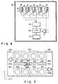
- Each of the coating section 10, the developing section 20 and the interface section 30 has an alkaline concentration analyzer 50.
- a detection terminal 53 of the concentration analyzer 50 is disposed in the upper space of each of the sections 10, 20 and 30 to detect the concentration of the alkaline component contained in air immediately after blown out from the filter unit 80.
- the "alkaline component" to be detected is organic amine, such as ammonia and NMP (N-methyl.2 pyrrolidinone), and their polar molecule components.
- the alkaline concentration analyzer 50 may be ion chromatography.
- a diffusion scrubber (not shown) and an auto-exchanger (not shown) are attached to the concentration analyzer 50.
- a tank 52 of the alkaline concentration analyzer 50 accommodates pure water 51.
- An end of a sampling pipe 54 is submerged in pure water 51 in the concentration analyzer 50.
- Another end 53 of the sampling pipe 54 is disposed above the resist coating units 15a and 15b and directly under the air blow-out opening of the air cleaning mechanism 80.
- An exhaust pipe 55 is submerged in pure water 51 in the concentration analyzer 50.
- Detection signals output from the alkaline concentration analyzer 50 are sequentially supplied to an input portion of a CPU 60.
- a memory portion of the CPU 60 previously stores a predetermined threshold value.
- the threshold value of the concentration of the alkaline component is determined to be 1 ppb.
- An output portion of the CPU 60 is connected to a monitor 70 and an alarm system 71.
- the alkaline concentration detected in each portion is displayed on the screen of the monitor 70 so that an operator of the system is permitted to immediately recognize the state of the system. If any one of the detected concentrations exceeds the threshold value, the CPU 60 operates the alarm system 71 to issue an alarm. If the threshold value is set to be lower than 1 ppb (for example, 0.7 ppb), a chemical filter 85 can be changed prior to occurrence of defective resolution with sufficient time margin.
- the CPU 60 feedback-controls the conveying machine 6 of the coating unit 10 and a drive motor 17 of a spin chuck 16. In accordance with a program transferred from the CPU 60, the process can be continued or interrupted.
- the wafer moving mechanism 2 takes out a non-processed wafer W from the first cassette 1a of the cassette station 4 in a loader/unloader section, and then places the non-processed wafer W on the holder 3 while centering the wafer W.
- the main conveying machine 6 picks up the wafer W from the holder 3 by the arm 7 and holds the same to introduce the wafer W into the processing section (step S1). Then, the main conveying machine 6 introduces the wafer W into the baking unit 13 to pre-bake the wafer W in accordance with a predetermined recipe (step S2).
- the wafer W is scrubbed with a brush in the scrubbing unit 11 (step S3), and then the wafer W is cleaned with jet water in a jet-water cleaning unit 14 (step S4).
- the wafer W is subjected to an adhesion process in the adhesion processing unit 12a (step S5).
- An alkaline component generated due to the adhesion process is brought to the air-discharge passage 88 in the floor portion by the downflow air. Then, the alkaline component is absorbed and removed by an alkaline component absorbing apparatus (not shown) disposed in the circulating circuit.
- the wafer W is cooled in the cooling portion 12b, and then a chemically amplified resist is applied to the wafer W in the resist coating units 15a and 15b (step S8).
- the reflection preventive resist may be applied to the wafer W (step S6) followed by baking the wafer W in accordance with the predetermined recipe (step S7).
- the chemically amplified resist is further applied onto the reflection preventive film (step S8).
- the alkaline component in supplied air is removed by the air cleaning mechanism 80 so as to lower the concentration of the alkaline component in the processing atmosphere to be lower than 1 ppb.
- the wafer W is again baked in the baking unit 13 (step S9). After the wafer W has been cooled in the cooling unit 12b, the wafer W is brought to the interface section 30 to align the position of the wafer W on the holder 31. Then, the wafer W is introduced into the exposing section 40 so as to be subjected to the exposing process (step S10).
- the wafer W is introduced into the baking unit 21 of the developing section 20 through the interface section 30 so as to be pre-baked before the developing process is performed (step S11). Then, the wafer W is developed in the developing unit 22 (step S12). Also the concentration of the alkaline component in the developing atmosphere is adjusted to be lower than 1 ppb by the air cleaning mechanism 80. After the developing process has been performed, the wafer W is post-baked in the baking unit 21 so that the sequential resist process is completed (step S13). The processed wafer W is moved to the cassette station 4 by the main conveying machine 6 so as to be placed on the holder 3. The wafer moving mechanism 2 accommodates the processed wafer W in the second cassette 1b. The processed wafer W is, while being accommodated in the second cassette 1b, taken out from the cassette station 4.
- the concentration of the alkaline component in the processing atmosphere is detected by the alkaline concentration analyzer 50 and the results of the detection are, in real time, displayed on the screen of the monitor 70 (step S14). If the chemical filter 85 deteriorates after it has been used for a long time and the performance for removing the alkaline component has deteriorated, the concentration of the alkaline component in the processing atmosphere is gradually raised.
- the CPU 60 compares the detected concentration of the alkaline component in the processing atmosphere and the threshold value (1 ppb) with each other. If the detected level is lower than the threshold value (1 ppb), the foregoing steps S1 to S13 are repeated (step S15). If the detected concentration of the alkaline component is higher than the threshold value (1 ppb), the CPU 60 issues a command to the alarm system 71 to issue an alarm (steps S15 and S16).
- the operator When the operator recognizes abnormal concentration of the alkaline component in the processing atmosphere in accordance with the alarm issued from the alarm system 71 and/or the screen of the monitor 70, the operator selects any one of the following methods (1), (2) and (3).
- the first method (1) enables the wafer W to be quickly and reliably protected from being damaged by the alkaline component in the atmosphere. However, since the wafer W, which is being processed in the processing sections 10 and 20, is collectively restored, the process involves waste.
- the second method (2) in which the wafer W, which is being processed in the processing sections 10 and 20, and the introduced non-processed wafer W are processed, enables the waste in the process to be prevented.
- the third method (3) is able to further prevent waste in the process as compared with the second method (2).
- a long time is required to interrupt the processing operation, there is a risk that the wafer W is damaged by the alkaline component in the atmosphere.
- each of the first to third methods (1), (2) and (3) has its merits and demerits.
- the threshold value of the concentration of the alkaline component in the processing atmosphere may be lowered from 1 ppb to 0.7 ppb.
- a structure may be employed in which, for example, five resist processing systems are included in single clean room 90; and the atmospheres of the processing sections 10, 20 and 30 of the five resist processing systems are, in parallel, controlled by using the common alkaline component concentration analyzer 50, the CPU 60, the monitor 70 and the alarm system 71.
- the CPU 60 controls the system to be adaptable to the difference.
- the threshold value of the concentration of the alkaline component in the former sections 10, 20, 30 is made to be 1 ppb and the threshold value of the concentration of the alkaline component in the latter section is made to be 10 ppb.
- the threshold value of the concentration of the alkaline component in the processing units 10 and 20 and the threshold value of the concentration of the alkaline component in the interface section 30 may be different from each other even in the same system.
- the concentration of the alkaline component in the processing atmosphere be detected at least from the resist coating step S8 to the developing step S12.
- the concentration of the alkaline component may be detected at a position near a door (not shown) in the system.
- the present invention may be applied when resist is applied to a glass substrate for LCD and the resist is developed.
- the concentration of the alkaline component in the processing atmosphere can be online-detected and the processing atmosphere for the substrate can quickly be improved in accordance with the detected value. Therefore, the manufacturing yield and the reliability of the apparatus can be improved.
- the operator Since the concentration of the alkaline component in the processing atmosphere is always monitored, the operator is able to predict the time at which the chemical filter must be changed and the life-time of the filter.
- the detected level of the concentration of the alkaline component in the processing atmosphere exceeds a threshold value, this fact is notified to the operator by the alarm system. Therefore, the operator is able to quickly takes a countermeasure against the problem. Thus, the damage of the chemically amplified resist applied to the wafer W can be prevented.
- the operator is able to analyze the state of the problem to detect the cause of the problem.
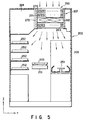
- FIGS. 5 to 9 another embodiment of the present invention will now be described.
- a resist processing system has a processing section 202, a loading/unloading section 221 and an interface section 222.
- An exposing portion (not shown) is connected to the interface section 222.
- the system is covered with a cover 206.
- the cover 206 has, in the upper portion, an air inlet opening 260.
- the air inlet opening 260 has three filter units 207.
- openings for introducing wafer are formed in the front and rear portions of the cover 206.
- Punching metal plates or gratings are disposed on the floors of the processing section 202, the loading/unloading section 221 and the interface section 222. Downflow air is arranged to flow from an upper filter unit 207 to pass through the processing space so as to be introduced into a position below the floor.
- the filter units 207 is surrounded by a case 272 and attached to the upper portion of the processing section 202.
- the outer case 272 accommodates a fan 262, a first filter portion 261 and a second filter portion 263.
- the first filter portion 261 is formed adjacent to the upper air inlet opening 260, while the second filter portion 263 is formed adjacent to the lower air inlet opening 260.
- the fan 262 is disposed between the first filter portion 261 and the second filter portion 263.
- Supplied air 280 is, through a common duct (not shown) of the plant, introduced into the first filter portion 261 in a direction indicated by arrows shown in FIGS. 8 and 9 to be allowed to pass through the upper first filter element 270. Then, supplied air 280 is allowed to pass through the lower fan 262 and the second filter element 271.
- the second filter portion 263 acts to remove particles from supplied air and has a filter element in the form of a sheet made of glass fiber.
- a gasket 274 be made of a material which does not considerably generate ammonia.
- silicon rubber or PVC be employed.
- the gasket 274 was submerged in a very pure water to measure the quantity of elution, a quantity of 20 ng/cm 2 was detected. If the quantity of elution of ammonia is the foregoing level, it can be said that the gasket 274 does not substantially generate ammonia in the atmosphere.
- the processing section 202 has, in the central portion thereof, a conveyance passage 231 extending in the direction of the X axis from an end 261 to another end 262.
- a main conveyance machine 203 is disposed so as to be capable of traveling along the conveyance passage 231.
- the main conveyance machine 203 has an arm for holding and moving the wafer W.
- the conveyance arm is able to move in the directions of the X, Y and Z axes.
- the conveyance arm is able to rotate around the Z axis by an angular degree of ⁇ .
- An adhesion unit 204, a resist coating unit 251, a heating unit 252, a cooling unit 253 and a developing unit 254 are disposed on the two sides of the conveyance passage 231.
- the first filter portion 261 has filter elements 270 and 271 stacked vertically. Supplied air 280 is initially allowed to pass through the first filter element 270, and then allowed to pass through the second filter element 271.
- Each of the first and second elements 270 and 271 is in the form of bellows made of a sheet, that is, projections 270a and 271a and recesses 270b and 271b are alternately repeated when viewed from supplied air 280 so as to be formed into a pleated shape.
- the recesses 271b of the second element are formed in the downstream portion of the projections 270a of the first element, while the projections 271a of the second element are formed in the downstream portion of the recesses 270b of the first element.
- Each of the elements 270 and 271 has a slit 273 through which air passes.
- the slit 273 of the first filter element 270 is formed in the upstream projection 270a, while the slit 273 of the second filter element 271 is formed in the downstream recess 271b.
- the side portion of the second filter element 271 is, through a seal layer 272a, attached to a support frame 272.
- the first and second elements 270 and 271 have substantially the same size.
- length L1 in the direction in which air flows is made to be about 70 mm
- bending interval L2 is made to be a pitch of about 4 mm
- the gap L3 is made to be about 5 mm or less.
- a gasket 274 is attached to a support frame 272 adjacent to the air outlet opening.
- Each of the first and second elements 270 and 271 is made of a carbon fiber sheet or an olefin fiber sheet. The foregoing fiber sheet is impregnated with phosphoric acid solution.
- the fiber sheet is submerged in phosphoric acid solution, and then the fiber sheet is set to a centrifugal separator so as to centrifugally separate and remove an excessive amount of the phosphoric acid solution. Then, the fiber sheet is pressed so as to be formed into a plate form. As a result of the pressing operation above, the concentration of small pores in the fiber sheet can be raised so that the shapes of the small pores are uniformed. Thus, the small pores are arranged regularly and the specific surface area can be enlarged.
- the ammonia component in supplied air 280 reacts with phosphoric acid contained in the first and second elements 270 and 271 and thus captured.
- the concentration of ammonia is finally lowered to a level of about 0.1 ppb.
- the performance of the first filter element 270 for removing ammonia deteriorates gradually due to use for a long time, the wanting of the removal performance of the first filter element 270 can be compensated by the second filter element 271.
- the first and second first filter elements 270 and 271 may be changed simultaneously.
- the second filter element 271 which is able to work, may be allowed to retain and only the first filter element 270 may be changed.
- the life-time of the chemical filter can significantly be elongated. Therefore, the frequency, at which the filter must be changed, can be lowered.
Landscapes
- Physics & Mathematics (AREA)
- General Physics & Mathematics (AREA)
- Health & Medical Sciences (AREA)
- Life Sciences & Earth Sciences (AREA)
- Atmospheric Sciences (AREA)
- Toxicology (AREA)
- Engineering & Computer Science (AREA)
- Environmental & Geological Engineering (AREA)
- Epidemiology (AREA)
- Public Health (AREA)
- Exposure Of Semiconductors, Excluding Electron Or Ion Beam Exposure (AREA)
- Photosensitive Polymer And Photoresist Processing (AREA)
Applications Claiming Priority (2)
| Application Number | Priority Date | Filing Date | Title |
|---|---|---|---|
| JP94752/96 | 1996-03-25 | ||
| JP09475296A JP3218425B2 (ja) | 1996-03-25 | 1996-03-25 | 処理方法及び処理装置 |
Publications (2)
| Publication Number | Publication Date |
|---|---|
| EP0798598A2 true EP0798598A2 (de) | 1997-10-01 |
| EP0798598A3 EP0798598A3 (de) | 1999-03-24 |
Family
ID=14118859
Family Applications (1)
| Application Number | Title | Priority Date | Filing Date |
|---|---|---|---|
| EP97105041A Withdrawn EP0798598A3 (de) | 1996-03-25 | 1997-03-25 | Verfahren zur Behandlung eines Photoresists auf einem Substrat und Einrichtung dafür |
Country Status (5)
| Country | Link |
|---|---|
| US (3) | US5932380A (de) |
| EP (1) | EP0798598A3 (de) |
| JP (1) | JP3218425B2 (de) |
| KR (1) | KR100357313B1 (de) |
| TW (1) | TW358220B (de) |
Cited By (2)
| Publication number | Priority date | Publication date | Assignee | Title |
|---|---|---|---|---|
| EP0908931A3 (de) * | 1997-10-07 | 2003-08-27 | Innotech Corporation | Fördervorrichtung |
| DE19901426B4 (de) * | 1998-04-21 | 2008-04-03 | Samsung Electronics Co., Ltd., Suwon | Mehrkammersystem einer Ätzeinrichtung zur Herstellung von Halbleiterbauelementen |
Families Citing this family (37)
| Publication number | Priority date | Publication date | Assignee | Title |
|---|---|---|---|---|
| TW444275B (en) | 1998-01-13 | 2001-07-01 | Toshiba Corp | Processing device, laser annealing device, laser annealing method, manufacturing device and substrate manufacturing device for panel display |
| JPH11274050A (ja) * | 1998-03-25 | 1999-10-08 | Canon Inc | 露光装置およびデバイス製造方法 |
| JP3422799B2 (ja) * | 1998-05-01 | 2003-06-30 | 東京エレクトロン株式会社 | 膜厚測定装置、基板処理方法並びに基板処理装置 |
| US6364762B1 (en) * | 1999-09-30 | 2002-04-02 | Lam Research Corporation | Wafer atmospheric transport module having a controlled mini-environment |
| US6355388B1 (en) * | 1999-10-07 | 2002-03-12 | Advanced Micro Devices, Inc. | Method for controlling photoresist strip processes |
| TW453612U (en) * | 2000-04-26 | 2001-09-01 | Ritdisplay Corp | Surface processing device of display panel |
| JP3590328B2 (ja) * | 2000-05-11 | 2004-11-17 | 東京エレクトロン株式会社 | 塗布現像処理方法及び塗布現像処理システム |
| US7404681B1 (en) * | 2000-05-31 | 2008-07-29 | Fsi International, Inc. | Coating methods and apparatus for coating |
| US6420098B1 (en) * | 2000-07-12 | 2002-07-16 | Motorola, Inc. | Method and system for manufacturing semiconductor devices on a wafer |
| US6368372B1 (en) * | 2000-08-08 | 2002-04-09 | Intrabay Automation, Inc. | Fluid media particle isolating system |
| US6379056B1 (en) * | 2000-09-12 | 2002-04-30 | Tokyo Electron Limited | Substrate processing apparatus |
| US6897165B2 (en) * | 2001-06-06 | 2005-05-24 | Matsushita Electric Industrial Co., Ltd. | Environmental control equipment/method of developing apparatus for developing light-exposed resist film with developer in wafer treating chamber |
| KR100517547B1 (ko) * | 2001-06-27 | 2005-09-28 | 삼성전자주식회사 | 포토레지스트 도포 장비 및 이 장비를 사용한포토레지스트 도포 방법 |
| US6864024B1 (en) * | 2002-11-22 | 2005-03-08 | Advanced Micro Devices, Inc. | Real-time control of chemically-amplified resist processing on wafer |
| US10517883B2 (en) * | 2003-06-27 | 2019-12-31 | Zuli Holdings Ltd. | Method of treating acute myocardial infarction |
| JP2005197362A (ja) | 2004-01-05 | 2005-07-21 | Toshiba Corp | 露光処理システムおよび露光処理方法 |
| JP4381285B2 (ja) * | 2004-11-11 | 2009-12-09 | 株式会社Sokudo | 基板処理装置および基板処理方法 |
| JP5154006B2 (ja) * | 2004-12-06 | 2013-02-27 | 株式会社Sokudo | 基板処理装置 |
| US7699021B2 (en) | 2004-12-22 | 2010-04-20 | Sokudo Co., Ltd. | Cluster tool substrate throughput optimization |
| US20060182535A1 (en) * | 2004-12-22 | 2006-08-17 | Mike Rice | Cartesian robot design |
| US7798764B2 (en) | 2005-12-22 | 2010-09-21 | Applied Materials, Inc. | Substrate processing sequence in a cartesian robot cluster tool |
| US20060130767A1 (en) | 2004-12-22 | 2006-06-22 | Applied Materials, Inc. | Purged vacuum chuck with proximity pins |
| US7819079B2 (en) | 2004-12-22 | 2010-10-26 | Applied Materials, Inc. | Cartesian cluster tool configuration for lithography type processes |
| US7651306B2 (en) | 2004-12-22 | 2010-01-26 | Applied Materials, Inc. | Cartesian robot cluster tool architecture |
| US20060241813A1 (en) * | 2005-04-22 | 2006-10-26 | Applied Materials, Inc. | Optimized cluster tool transfer process and collision avoidance design |
| US20080051930A1 (en) * | 2006-07-10 | 2008-02-28 | Oh Hilario L | Scheduling method for processing equipment |
| US7522968B2 (en) * | 2006-07-10 | 2009-04-21 | Applied Materials, Inc. | Scheduling method for processing equipment |
| WO2008008727A2 (en) * | 2006-07-10 | 2008-01-17 | Applied Materials, Inc. | Scheduling method for processing equipment |
| JP2008103384A (ja) * | 2006-10-17 | 2008-05-01 | Elpida Memory Inc | レジストパターンの形成方法およびレジスト塗布現像装置 |
| JP4359640B2 (ja) * | 2007-09-25 | 2009-11-04 | 東京エレクトロン株式会社 | 基板搬送装置及びダウンフロー制御方法 |
| US9117870B2 (en) * | 2008-03-27 | 2015-08-25 | Lam Research Corporation | High throughput cleaner chamber |
| US8562272B2 (en) * | 2010-02-16 | 2013-10-22 | Lam Research Corporation | Substrate load and unload mechanisms for high throughput |
| US8282698B2 (en) * | 2010-03-24 | 2012-10-09 | Lam Research Corporation | Reduction of particle contamination produced by moving mechanisms in a process tool |
| US8893642B2 (en) | 2010-03-24 | 2014-11-25 | Lam Research Corporation | Airflow management for low particulate count in a process tool |
| JP5817693B2 (ja) * | 2012-09-25 | 2015-11-18 | 東京エレクトロン株式会社 | 基板処理装置 |
| US9272315B2 (en) * | 2013-10-11 | 2016-03-01 | Taiwan Semiconductor Manufacturing Co., Ltd | Mechanisms for controlling gas flow in enclosure |
| JP6736087B2 (ja) * | 2017-01-23 | 2020-08-05 | 株式会社平間理化研究所 | 現像液の濃度監視装置、及び現像液管理装置 |
Family Cites Families (6)
| Publication number | Priority date | Publication date | Assignee | Title |
|---|---|---|---|---|
| US5143552A (en) * | 1988-03-09 | 1992-09-01 | Tokyo Electron Limited | Coating equipment |
| JP2559617B2 (ja) * | 1988-03-24 | 1996-12-04 | キヤノン株式会社 | 基板処理装置 |
| US5326316A (en) * | 1991-04-17 | 1994-07-05 | Matsushita Electric Industrial Co., Ltd. | Coupling type clean space apparatus |
| JP3152779B2 (ja) * | 1993-01-08 | 2001-04-03 | 株式会社東芝 | レジスト処理方法及びレジスト処理装置 |
| KR100242530B1 (ko) * | 1993-05-18 | 2000-02-01 | 히가시 데쓰로 | 필터장치 |
| JP3500619B2 (ja) * | 1993-10-28 | 2004-02-23 | 株式会社ニコン | 投影露光装置 |
-
1996
- 1996-03-25 JP JP09475296A patent/JP3218425B2/ja not_active Expired - Fee Related
-
1997
- 1997-03-21 TW TW086103595A patent/TW358220B/zh active
- 1997-03-24 US US08/823,470 patent/US5932380A/en not_active Expired - Lifetime
- 1997-03-25 KR KR1019970010284A patent/KR100357313B1/ko not_active Expired - Fee Related
- 1997-03-25 EP EP97105041A patent/EP0798598A3/de not_active Withdrawn
-
1999
- 1999-03-29 US US09/277,734 patent/US6097469A/en not_active Expired - Lifetime
- 1999-03-29 US US09/277,735 patent/US6017663A/en not_active Expired - Fee Related
Cited By (2)
| Publication number | Priority date | Publication date | Assignee | Title |
|---|---|---|---|---|
| EP0908931A3 (de) * | 1997-10-07 | 2003-08-27 | Innotech Corporation | Fördervorrichtung |
| DE19901426B4 (de) * | 1998-04-21 | 2008-04-03 | Samsung Electronics Co., Ltd., Suwon | Mehrkammersystem einer Ätzeinrichtung zur Herstellung von Halbleiterbauelementen |
Also Published As
| Publication number | Publication date |
|---|---|
| US6017663A (en) | 2000-01-25 |
| JPH09260275A (ja) | 1997-10-03 |
| TW358220B (en) | 1999-05-11 |
| KR970067586A (ko) | 1997-10-13 |
| EP0798598A3 (de) | 1999-03-24 |
| US5932380A (en) | 1999-08-03 |
| JP3218425B2 (ja) | 2001-10-15 |
| US6097469A (en) | 2000-08-01 |
| KR100357313B1 (ko) | 2003-01-24 |
Similar Documents
| Publication | Publication Date | Title |
|---|---|---|
| US5932380A (en) | Method of processing resist utilizing alkaline component monitoring | |
| EP0756315B1 (de) | Eine Vorrichtung zur Photolackbearbeitung und ein Verfahren zur Photolackbearbeitung | |
| KR100503121B1 (ko) | 처리장치및처리방법 | |
| US20070127916A1 (en) | Substrate processing apparatus and substrate processing method | |
| KR100242530B1 (ko) | 필터장치 | |
| CN111433888A (zh) | 液供给装置和液供给方法 | |
| EP1164438B1 (de) | Entwicklungsverfahren und -vorrichtung | |
| US20020144719A1 (en) | Solution treatment unit | |
| US4993271A (en) | Liquid in situ multiport monitoring system | |
| US6473151B1 (en) | Substrate processing apparatus | |
| JP3342838B2 (ja) | 処理装置および処理方法 | |
| JP4628623B2 (ja) | ウェハ洗浄システムの処理前調整を実施する方法 | |
| CN101505884A (zh) | 用于显影光刻胶的装置以及用于操作该装置的方法 | |
| JPH04326509A (ja) | ホトレジスト処理方法および装置ならびに基板保管装置 | |
| JPH09275055A (ja) | 露光装置 | |
| JP2002501298A (ja) | リニアディベロッパ | |
| JP3469803B2 (ja) | 塗布、現像装置の運転方法及び塗布、現像装置 | |
| JP4731377B2 (ja) | 基板処理装置および基板処理方法 | |
| JPS5856251B2 (ja) | 複数基板の一括処理装置 | |
| JP3145576B2 (ja) | 表面処理装置 | |
| JP2810680B2 (ja) | 露光装置及び露光方法 | |
| JP3094055B2 (ja) | フィルタ装置及びレジスト処理システム | |
| JPH09298148A (ja) | 露光方法及び露光装置 | |
| KR102624575B1 (ko) | 기판 처리 장치 및 압력 측정 방법 | |
| JPH1076213A (ja) | 塗布方法及び塗布装置 |
Legal Events
| Date | Code | Title | Description |
|---|---|---|---|
| PUAI | Public reference made under article 153(3) epc to a published international application that has entered the european phase |
Free format text: ORIGINAL CODE: 0009012 |
|
| AK | Designated contracting states |
Kind code of ref document: A2 Designated state(s): DE GB |
|
| PUAL | Search report despatched |
Free format text: ORIGINAL CODE: 0009013 |
|
| AK | Designated contracting states |
Kind code of ref document: A3 Designated state(s): DE GB |
|
| 17P | Request for examination filed |
Effective date: 19990707 |
|
| 17Q | First examination report despatched |
Effective date: 20040122 |
|
| STAA | Information on the status of an ep patent application or granted ep patent |
Free format text: STATUS: THE APPLICATION IS DEEMED TO BE WITHDRAWN |
|
| 18D | Application deemed to be withdrawn |
Effective date: 20121001 |