EP0798771A2 - Silizium-Wafer mit einer amorphen Siliziumschicht und Verfahren zur Herstellung derselben durch plasma-aktivierte chemische Dampfabscheidung (PECVD) - Google Patents
Silizium-Wafer mit einer amorphen Siliziumschicht und Verfahren zur Herstellung derselben durch plasma-aktivierte chemische Dampfabscheidung (PECVD) Download PDFInfo
- Publication number
- EP0798771A2 EP0798771A2 EP97302062A EP97302062A EP0798771A2 EP 0798771 A2 EP0798771 A2 EP 0798771A2 EP 97302062 A EP97302062 A EP 97302062A EP 97302062 A EP97302062 A EP 97302062A EP 0798771 A2 EP0798771 A2 EP 0798771A2
- Authority
- EP
- European Patent Office
- Prior art keywords
- silicon wafer
- amorphous silicon
- vapor deposition
- silicon layer
- chemical vapor
- Prior art date
- Legal status (The legal status is an assumption and is not a legal conclusion. Google has not performed a legal analysis and makes no representation as to the accuracy of the status listed.)
- Withdrawn
Links
Images


Classifications
-
- H—ELECTRICITY
- H10—SEMICONDUCTOR DEVICES; ELECTRIC SOLID-STATE DEVICES NOT OTHERWISE PROVIDED FOR
- H10P—GENERIC PROCESSES OR APPARATUS FOR THE MANUFACTURE OR TREATMENT OF DEVICES COVERED BY CLASS H10
- H10P90/00—Preparation of wafers not covered by a single main group of this subclass, e.g. wafer reinforcement
- H10P90/12—Preparing bulk and homogeneous wafers
-
- H—ELECTRICITY
- H10—SEMICONDUCTOR DEVICES; ELECTRIC SOLID-STATE DEVICES NOT OTHERWISE PROVIDED FOR
- H10P—GENERIC PROCESSES OR APPARATUS FOR THE MANUFACTURE OR TREATMENT OF DEVICES COVERED BY CLASS H10
- H10P14/00—Formation of materials, e.g. in the shape of layers or pillars
- H10P14/20—Formation of materials, e.g. in the shape of layers or pillars of semiconductor materials
- H10P14/24—Formation of materials, e.g. in the shape of layers or pillars of semiconductor materials using chemical vapour deposition [CVD]
-
- H—ELECTRICITY
- H10—SEMICONDUCTOR DEVICES; ELECTRIC SOLID-STATE DEVICES NOT OTHERWISE PROVIDED FOR
- H10P—GENERIC PROCESSES OR APPARATUS FOR THE MANUFACTURE OR TREATMENT OF DEVICES COVERED BY CLASS H10
- H10P14/00—Formation of materials, e.g. in the shape of layers or pillars
- H10P14/20—Formation of materials, e.g. in the shape of layers or pillars of semiconductor materials
- H10P14/29—Formation of materials, e.g. in the shape of layers or pillars of semiconductor materials characterised by the substrates
- H10P14/2901—Materials
- H10P14/2902—Materials being Group IVA materials
- H10P14/2905—Silicon, silicon germanium or germanium
-
- H—ELECTRICITY
- H10—SEMICONDUCTOR DEVICES; ELECTRIC SOLID-STATE DEVICES NOT OTHERWISE PROVIDED FOR
- H10P—GENERIC PROCESSES OR APPARATUS FOR THE MANUFACTURE OR TREATMENT OF DEVICES COVERED BY CLASS H10
- H10P14/00—Formation of materials, e.g. in the shape of layers or pillars
- H10P14/20—Formation of materials, e.g. in the shape of layers or pillars of semiconductor materials
- H10P14/34—Deposited materials, e.g. layers
- H10P14/3402—Deposited materials, e.g. layers characterised by the chemical composition
- H10P14/3404—Deposited materials, e.g. layers characterised by the chemical composition being Group IVA materials
- H10P14/3411—Silicon, silicon germanium or germanium
-
- H—ELECTRICITY
- H10—SEMICONDUCTOR DEVICES; ELECTRIC SOLID-STATE DEVICES NOT OTHERWISE PROVIDED FOR
- H10P—GENERIC PROCESSES OR APPARATUS FOR THE MANUFACTURE OR TREATMENT OF DEVICES COVERED BY CLASS H10
- H10P36/00—Gettering within semiconductor bodies
- H10P36/03—Gettering within semiconductor bodies within silicon bodies
-
- Y—GENERAL TAGGING OF NEW TECHNOLOGICAL DEVELOPMENTS; GENERAL TAGGING OF CROSS-SECTIONAL TECHNOLOGIES SPANNING OVER SEVERAL SECTIONS OF THE IPC; TECHNICAL SUBJECTS COVERED BY FORMER USPC CROSS-REFERENCE ART COLLECTIONS [XRACs] AND DIGESTS
- Y10—TECHNICAL SUBJECTS COVERED BY FORMER USPC
- Y10S—TECHNICAL SUBJECTS COVERED BY FORMER USPC CROSS-REFERENCE ART COLLECTIONS [XRACs] AND DIGESTS
- Y10S438/00—Semiconductor device manufacturing: process
- Y10S438/977—Thinning or removal of substrate
Definitions
- the present invention relates to a silicon wafer and its manufacturing method. More particularly, the present invention relates to a silicon wafer having an amorphous silicon layer, formed as a gettering layer, on the main surface (hereinafter referred to as a "reverse surface") opposite to the main surface (hereinafter referred to as a "front surface”) on which semiconductor devices will be fabricated, as well as to a method of manufacturing the silicon wafer.
- impurities such as heavy metals are generated during fabrication of a semiconductor device from a silicon wafer, and the thus-generated impurities contaminate the vicinity of the surface of a silicon wafer which will become an active area in the semiconductor device. If the vicinity of the surface of the silicon wafer which will become an active area is contaminated by impurities, the characteristics of the device are degraded, which in turn reduces the proportion of non-defective devices.
- a technique of intentionally collecting impurities outside of the active area namely, a gettering technique
- a representative method of the gettering technique is the forming of a polycrystalline silicon layer as a gettering layer on the reverse surface of a silicon wafer.
- a polycrystalline silicon layer is usually formed by growing polycrystalline silicon on the reverse surface of the silicon using a LPCVD (Low Pressure Chemical Vapor Deposition) method.
- LPCVD Low Pressure Chemical Vapor Deposition
- the silicon wafer having a polycrystalline layer formed on the reverse surface thereof undergoes stress. Compared with a silicon wafer without a polycrystalline silicon layer, the silicon wafer having a polycrystalline layer becomes warped to a greater extent. If polycrystalline silicon is grown on the reverse surfaces of silicon wafers of different diameters under the same conditions, the warpage increases with the diameter of the silicon wafer. Associated with a recent tendency of a semiconductor device to be highly integrated with higher accuracy, the diameter of the silicon wafer is steadily increasing. Because of this, it is to be desired that the warpage of the silicon wafer be reduced to as small an extent as possible.
- a polycrystalline silicon layer is formed on a silicon wafer under conditions such that the stress acting on the silicon wafer decreases.
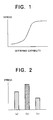
- the polycrystalline silicon layer is formed on the silicon wafer at a high temperature such that the grain size of polycrystalline silicon becomes greater, or the polycrystalline silicon layer is formed so as to become thinner. In these cases, however, the gettering capability of the polycrystalline silicon layer is decreased, as shown in FIG. 1.
- the polycrystalline silicon layer As a polycrystalline silicon layer is subjected to heat treatment during fabrication of semiconductor devices from a silicon wafer, the polycrystalline silicon layer is further crystallized into monocrystal, thereby resulting in a reduction in the gettering capability of the polycrystalline silicon layer.
- the amorphous silicon layer has the advantage of being resistant to crystallization into monocrystal relative to the polycrystalline silicon layer, even when it is subjected to heat treatment during the fabrication of semiconductor devices, thus providing the advantage of longer continuance of the gettering capability.
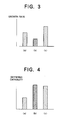
- an amorphous silicon layer is formed (designated by (b) in FIG. 2) by growing amorphous silicon on the reverse surface of the silicon wafer using the low pressure chemical vapor deposition method in the same way as for polycrystalline silicon, the stress acting on the silicon wafer becomes larger than the stress resulting from formation of a polycrystalline silicon layer (designated by (a) in FIG. 2). As a result, the warpage of the silicon wafer becomes still greater.
- FIG. 1 as is the case of formation of a polycrystalline silicon layer, even if an amorphous silicon layer is formed using the low pressure chemical vapor deposition method, the stress acting on the silicon wafer increases so long as the gettering capability of the amorphous silicon layer increases.
- a growth rate of the amorphous silicon becomes extremely low as compared with that of the polycrystalline silicon (designated by (a) in FIG. 3), thereby resulting in a decrease in the productivity of a silicon wafer.
- an amorphous silicon layer is formed by growing amorphous silicon on the reverse surface of a silicon wafer using a plasma chemical vapor deposition method in lieu of the low pressure chemical vapor deposition method,
- the amorphous silicon layer is formed using the plasma chemical vapor deposition method, the stress acting on the silicon wafer can be reduced, and the gettering capability of the amorphous silicon layer can be improved, as well.
- These effects are amazing and are completely contrast to the tendency in the case where a polycrystalline silicon layer or an amorphous silicon layer is formed using the low pressure chemical vapor deposition method; i.e., the tendency of the gettering capability of the polycrystalline silicon layer to decrease with a decrease in the stress acting on the silicon wafer, as illustrated in FIG. 1. It is considered that a large amount of hydrogen atoms contained in the amorphous silicon formed by the use of the plasma chemical vapor deposition method contribute to improved continuance of the gettering capability.
- an object of the present invention is to provide a silicon wafer which has a gettering layer possessing high gettering capability and enhanced continuance of the gettering capability and which undergoes reduced stress due to the gettering layer so that its warpage decreases.
- Another object of the present invention is to provide a method of manufacturing such an improved silicon wafer with high productivity.
- the present invention provides a silicon wafer having an amorphous silicon layer formed on one main surface thereof.
- the amorphous silicon layer is formed by plasma chemical vapor deposition.
- the present invention also provides the following manufacturing methods:
- the main surface of the silicon wafer on which the amorphous silicon layer is to be formed is an etched or mirror-polished surface.
- the present invention it is possible to provide a silicon wafer which has a gettering layer possessing high gettering capability and enhanced continuance of the gettering capability and which undergoes reduced stress due to the gettering layer so that its warpage decreases.
- a method of manufacturing a silicon wafer usually comprises a slicing process A for slicing a silicon monocrystalline rod manufactured by a monocrystal manufacturing apparatus into disk-shaped silicon wafers; a chamfering process B for chamfering the outer edge of each of the silicon wafers thus sliced in the slicing process A in order to prevent the silicon wafer from becoming cracked or chipped; a lapping process C for lapping the thus-chamfered silicon wafer so as to form a flat surface thereon; an etching process D for eliminating mechanical damage remaining in both the front and reverse surfaces of the chamfered and lapped silicon wafer; a mirror-polishing process E for polishing the surface of the etched silicon wafer; and a cleaning process F for cleaning the mirror-polished surface of the silicon wafer so as to remove polishing material and foreign matter adhered thereto.
- a silicon wafer having an amorphous silicon layer formed on the reverse surface thereof according to the present invention is usually manufactured by forming an amorphous silicon layer on the reverse surface of the silicon wafer through use of the plasma chemical vapor deposition method after having etched it in the etching process D, and by subsequently subjecting the thus-formed amorphous silicon layer to the mirror-polishing process E and the cleaning process F.
- an amorphous silicon layer is formed on the reverse surface of the silicon wafer using the plasma chemical vapor deposition method, an amorphous silicon layer continued to the amorphous silicon layer on the reverse surface is unintentionally formed on the front surface. Even in this case, the thus-formed amorphous silicon layer on the front surface is eliminated by the mirror-polishing process E.
- the polishing be performed as less as possible in order to maintain the flatness of the surface. For this reason, it is preferred that the amorphous silicon layer formed on the front surface is soft (i.e., a quick polishing is desirable). Since the amorphous silicon layer formed using the plasma chemical vapor deposition method is soft and it can be polished quick, the silicon wafer formed according to the present invention is very superior even in this respect.
- an amorphous silicon layer on the reverse surface of the silicon wafer using the plasma chemical vapor deposition method after the front surface of or the front and reverse surfaces of the etched silicon wafer have been mirror-polished.
- the amorphous silicon layer is formed solely on the reverse surface of the silicon wafer so that no amorphous silicon layer is formed on the front surface thereof, the silicon wafer can proceed to the cleaning process F without need for second mirror-polishing (re-mirror-polishing) of the front surface of the silicon wafer, as illustrated in FIG. 7B.
- the amorphous silicon layer is usually formed on the reverse surface of the silicon wafer, using a plasma chemical vapor deposition apparatus which utilizes the plasma chemical vapor deposition method.
- the amorphous silicon layer can be utilized in preventing an epitaxial wafer from autodoping during epitaxial growth of an epitaxial layer using a high-doped substrate.
- Amorphous silicon and polycrystalline silicon were compared with each other with regard to growth rate, stress acting on a silicon wafer, and gettering capability of a gettering layer.
- silicon wafers were sliced from a silicon monocrystal rod manufactured by a floating zone method (a p-type conductivity). The thus-sliced silicon wafers were subjected to chamfering, lapping, and etching processing.
- a silicon wafer sliced from a silicon monocrystal rod manufactured by a CZ method possesses an intrinsic gettering effect and, hence, is unsuitable for use in checking the gettering capability of a gettering layer. For this reason, there were used the silicon wafers which were formed from the silicon monocrystal rod manufactured by the floating zone method and which did not have any intrinsic gettering effect.
- a silicon monocrystal rod manufactured by a CZ method is suitable for an actual application.
- An amorphous silicon layer serving as a gettering layer was formed on the reverse surface of a wafer under growth conditions shown in table 1, using a plasma chemical vapor deposition apparatus using radio-frequency of 13.56 MHz (made by Novellus Systems Inc.).
- a polycrystalline silicon layer serving as a gettering layer was formed on the reverse surface of a wafer under the growth conditions shown in table 1, using a low pressure chemical vapor deposition apparatus (made by Shinko Denki Corporation).
- An amorphous silicon layer serving as a gettering layer was formed on the reverse surface of a wafer under the growth conditions shown in table 1, using the low pressure chemical vapor deposition apparatus (made by Shinko Denki Corporation).
- the warpage of each silicon wafer was measured before and after the formation of its gettering layer, and the magnitude of the stress acting on the silicon wafer was calculated from the difference between the measured warpages before and after the formation of the getting layer.
- a ratio of iron captured by the gettering layer was calculated from a measurement value of the concentration of iron. The thus-calculated ratio was used as the gettering capability.
- Table 2 shows the results of the measurement of the amorphous silicon and the polycrystalline silicon with regard to the growth rate, the stress acting on the silicon wafer and the gettering capability of the gettering layer.
- Growth rate (nm/min.) Stress (Pa) Gettering capability (%)
- Example of the Invention 100 2 ⁇ 10 8 99 Comparative Example 1 20 5 ⁇ 10 8 93 Comparative Example 2 3 7 ⁇ 10 8 99
Applications Claiming Priority (2)
| Application Number | Priority Date | Filing Date | Title |
|---|---|---|---|
| JP99370/96 | 1996-03-28 | ||
| JP8099370A JPH09266212A (ja) | 1996-03-28 | 1996-03-28 | シリコンウエーハおよびその製造方法 |
Publications (2)
| Publication Number | Publication Date |
|---|---|
| EP0798771A2 true EP0798771A2 (de) | 1997-10-01 |
| EP0798771A3 EP0798771A3 (de) | 1997-10-08 |
Family
ID=14245662
Family Applications (1)
| Application Number | Title | Priority Date | Filing Date |
|---|---|---|---|
| EP97302062A Withdrawn EP0798771A3 (de) | 1996-03-28 | 1997-03-26 | Silizium-Wafer mit einer amorphen Siliziumschicht und Verfahren zur Herstellung derselben durch plasma-aktivierte chemische Dampfabscheidung (PECVD) |
Country Status (4)
| Country | Link |
|---|---|
| US (1) | US5970365A (de) |
| EP (1) | EP0798771A3 (de) |
| JP (1) | JPH09266212A (de) |
| TW (1) | TW430903B (de) |
Cited By (2)
| Publication number | Priority date | Publication date | Assignee | Title |
|---|---|---|---|---|
| US6027569A (en) * | 1998-06-03 | 2000-02-22 | Seh America, Inc. | Gas injection systems for a LPCVD furnace |
| WO2002052643A3 (en) * | 2000-12-27 | 2003-03-06 | Memc Electronic Materials | Semiconductor wafer manufacturing process |
Families Citing this family (6)
| Publication number | Priority date | Publication date | Assignee | Title |
|---|---|---|---|---|
| JP2004531048A (ja) * | 2000-12-15 | 2004-10-07 | サイバーオプティクス コーポレーション | 改良されたインタフェースを有する基板整列画像捕捉装置 |
| US20020080236A1 (en) * | 2000-12-15 | 2002-06-27 | Madsen David D. | Camera with improved illuminator |
| JP2002231665A (ja) * | 2001-02-06 | 2002-08-16 | Sumitomo Metal Ind Ltd | エピタキシャル膜付き半導体ウエーハの製造方法 |
| US6582995B2 (en) * | 2001-07-11 | 2003-06-24 | Taiwan Semiconductor Manufacturing Co., Ltd. | Method for fabricating a shallow ion implanted microelectronic structure |
| US8846500B2 (en) | 2010-12-13 | 2014-09-30 | Semiconductor Components Industries, Llc | Method of forming a gettering structure having reduced warpage and gettering a semiconductor wafer therewith |
| JP7683803B1 (ja) * | 2024-12-20 | 2025-05-27 | 信越半導体株式会社 | エピタキシャルウェーハの製造方法 |
Family Cites Families (11)
| Publication number | Priority date | Publication date | Assignee | Title |
|---|---|---|---|---|
| AT380974B (de) * | 1982-04-06 | 1986-08-11 | Shell Austria | Verfahren zum gettern von halbleiterbauelementen |
| JPS60119733A (ja) * | 1983-12-01 | 1985-06-27 | Fuji Electric Corp Res & Dev Ltd | シリコン板の重金属ゲッタリング方法 |
| JPS6124240A (ja) * | 1984-07-13 | 1986-02-01 | Toshiba Corp | 半導体基板 |
| JPH042133A (ja) * | 1990-04-18 | 1992-01-07 | Mitsubishi Electric Corp | 結晶板 |
| JP2583803B2 (ja) * | 1990-06-08 | 1997-02-19 | 東芝セラミックス株式会社 | アモルファス構造を有するウェーハ |
| JP3063143B2 (ja) * | 1990-10-29 | 2000-07-12 | 日本電気株式会社 | Si基板の製造方法 |
| JP2726583B2 (ja) * | 1991-11-18 | 1998-03-11 | 三菱マテリアルシリコン株式会社 | 半導体基板 |
| DE4304849C2 (de) * | 1992-02-21 | 2000-01-27 | Mitsubishi Electric Corp | Halbleitervorrichtung und Verfahren zur Herstellung einer Halbleitervorrichtung |
| JP2839801B2 (ja) * | 1992-09-18 | 1998-12-16 | 三菱マテリアル株式会社 | ウェーハの製造方法 |
| JPH07221112A (ja) * | 1994-02-02 | 1995-08-18 | Hitachi Ltd | 半導体ウエーハの製造方法 |
| US5757063A (en) * | 1994-03-25 | 1998-05-26 | Kabushiki Kaisha Toshiba | Semiconductor device having an extrinsic gettering film |
-
1996
- 1996-03-28 JP JP8099370A patent/JPH09266212A/ja active Pending
-
1997
- 1997-03-24 TW TW086103680A patent/TW430903B/zh not_active IP Right Cessation
- 1997-03-24 US US08/826,441 patent/US5970365A/en not_active Expired - Fee Related
- 1997-03-26 EP EP97302062A patent/EP0798771A3/de not_active Withdrawn
Cited By (2)
| Publication number | Priority date | Publication date | Assignee | Title |
|---|---|---|---|---|
| US6027569A (en) * | 1998-06-03 | 2000-02-22 | Seh America, Inc. | Gas injection systems for a LPCVD furnace |
| WO2002052643A3 (en) * | 2000-12-27 | 2003-03-06 | Memc Electronic Materials | Semiconductor wafer manufacturing process |
Also Published As
| Publication number | Publication date |
|---|---|
| JPH09266212A (ja) | 1997-10-07 |
| EP0798771A3 (de) | 1997-10-08 |
| US5970365A (en) | 1999-10-19 |
| TW430903B (en) | 2001-04-21 |
Similar Documents
| Publication | Publication Date | Title |
|---|---|---|
| US5738942A (en) | Semiconductor silicon wafer and process for producing it | |
| CA1121521A (en) | Semiconductor substrate and a manufacturing method thereof | |
| US7579261B2 (en) | Epitaxially coated silicon wafer and method for producing epitaxially coated silicon wafers | |
| KR101101480B1 (ko) | 에피택셜 코팅 실리콘 웨이퍼의 제조 방법 | |
| US5834363A (en) | Method of manufacturing semiconductor wafer, semiconductor wafer manufactured by the same, semiconductor epitaxial wafer, and method of manufacturing the semiconductor epitaxial wafer | |
| US6995077B2 (en) | Epitaxially coated semiconductor wafer and process for producing it | |
| EP2159826A1 (de) | Verfahren zur herstellung von soi-wafern | |
| SG183019A1 (en) | Epitaxially coated silicon wafer and method for producing epitaxially coated silicon wafers | |
| KR20060017676A (ko) | 실리콘 웨이퍼의 제조방법, 및 실리콘 웨이퍼와 soi웨이퍼 | |
| EP1758154B1 (de) | Herstellungsverfahren für einen siliziumwafer | |
| US5389551A (en) | Method of manufacturing a semiconductor substrate | |
| JP3454033B2 (ja) | シリコンウェーハおよびその製造方法 | |
| JPH03295235A (ja) | エピタキシャルウェーハの製造方法 | |
| EP1533402B1 (de) | Epitaktischer wafer und herstellungsverfahren dafür | |
| US5970365A (en) | Silicon wafer including amorphous silicon layer formed by PCVD and method of manufacturing wafer | |
| US11990336B2 (en) | Silicon epitaxial wafer production method and silicon epitaxial wafer | |
| EP0798770B1 (de) | Siliziumscheibe mit auf einer Oberfläche gestapelten polykristallinen Siliziumschichten,und ihr Herstellungsverfahren | |
| US6965149B2 (en) | Epitaxial semiconductor wafer and a manufacturing method thereof | |
| JP5347791B2 (ja) | 半導体エピタキシャルウエーハの製造方法 | |
| US6576501B1 (en) | Double side polished wafers having external gettering sites, and method of producing same | |
| US20080003782A1 (en) | Multilayer gettering structure for semiconductor device and method | |
| KR101063908B1 (ko) | 에피택셜 웨이퍼의 제조장치 및 방법 | |
| KR20090116646A (ko) | 실리콘 웨이퍼 및 이의 제조방법 | |
| KR20050032837A (ko) | 에피택셜 웨이퍼의 제조방법 | |
| CN118048691A (zh) | 层叠晶片的制造方法和层叠晶片 |
Legal Events
| Date | Code | Title | Description |
|---|---|---|---|
| PUAI | Public reference made under article 153(3) epc to a published international application that has entered the european phase |
Free format text: ORIGINAL CODE: 0009012 |
|
| PUAL | Search report despatched |
Free format text: ORIGINAL CODE: 0009013 |
|
| AK | Designated contracting states |
Kind code of ref document: A2 Designated state(s): DE FR GB |
|
| AK | Designated contracting states |
Kind code of ref document: A3 Designated state(s): DE FR GB |
|
| 17P | Request for examination filed |
Effective date: 19971120 |
|
| 17Q | First examination report despatched |
Effective date: 20001027 |
|
| STAA | Information on the status of an ep patent application or granted ep patent |
Free format text: STATUS: THE APPLICATION IS DEEMED TO BE WITHDRAWN |
|
| 18D | Application deemed to be withdrawn |
Effective date: 20021101 |