EP0798840A2 - Batterie-Stromversorgung - Google Patents
Batterie-Stromversorgung Download PDFInfo
- Publication number
- EP0798840A2 EP0798840A2 EP97104065A EP97104065A EP0798840A2 EP 0798840 A2 EP0798840 A2 EP 0798840A2 EP 97104065 A EP97104065 A EP 97104065A EP 97104065 A EP97104065 A EP 97104065A EP 0798840 A2 EP0798840 A2 EP 0798840A2
- Authority
- EP
- European Patent Office
- Prior art keywords
- converter
- switching element
- power supply
- battery power
- battery
- Prior art date
- Legal status (The legal status is an assumption and is not a legal conclusion. Google has not performed a legal analysis and makes no representation as to the accuracy of the status listed.)
- Granted
Links
Images
Classifications
-
- H—ELECTRICITY
- H02—GENERATION; CONVERSION OR DISTRIBUTION OF ELECTRIC POWER
- H02J—ELECTRIC POWER NETWORKS; CIRCUIT ARRANGEMENTS OR SYSTEMS FOR SUPPLYING OR DISTRIBUTING ELECTRIC POWER; SYSTEMS FOR STORING ELECTRIC ENERGY
- H02J7/00—Circuit arrangements for charging or discharging batteries or for supplying loads from batteries
- H02J7/34—Parallel operation in networks using both storage and other DC sources, e.g. providing buffering
- H02J7/345—Parallel operation in networks using both storage and other DC sources, e.g. providing buffering using capacitors as storage or buffering devices
-
- H—ELECTRICITY
- H02—GENERATION; CONVERSION OR DISTRIBUTION OF ELECTRIC POWER
- H02M—APPARATUS FOR CONVERSION BETWEEN AC AND AC, BETWEEN AC AND DC, OR BETWEEN DC AND DC, AND FOR USE WITH MAINS OR SIMILAR POWER SUPPLY SYSTEMS; CONVERSION OF DC OR AC INPUT POWER INTO SURGE OUTPUT POWER; CONTROL OR REGULATION THEREOF
- H02M3/00—Conversion of DC power input into DC power output
- H02M3/02—Conversion of DC power input into DC power output without intermediate conversion into AC
- H02M3/04—Conversion of DC power input into DC power output without intermediate conversion into AC by static converters
- H02M3/10—Conversion of DC power input into DC power output without intermediate conversion into AC by static converters using discharge tubes with control electrode or semiconductor devices with control electrode
- H02M3/145—Conversion of DC power input into DC power output without intermediate conversion into AC by static converters using discharge tubes with control electrode or semiconductor devices with control electrode using devices of a triode or transistor type requiring continuous application of a control signal
- H02M3/155—Conversion of DC power input into DC power output without intermediate conversion into AC by static converters using discharge tubes with control electrode or semiconductor devices with control electrode using devices of a triode or transistor type requiring continuous application of a control signal using semiconductor devices only
- H02M3/156—Conversion of DC power input into DC power output without intermediate conversion into AC by static converters using discharge tubes with control electrode or semiconductor devices with control electrode using devices of a triode or transistor type requiring continuous application of a control signal using semiconductor devices only with automatic control of output voltage or current, e.g. switching regulators
- H02M3/158—Conversion of DC power input into DC power output without intermediate conversion into AC by static converters using discharge tubes with control electrode or semiconductor devices with control electrode using devices of a triode or transistor type requiring continuous application of a control signal using semiconductor devices only with automatic control of output voltage or current, e.g. switching regulators including plural semiconductor devices as final control devices for a single load
- H02M3/1582—Buck-boost converters
Definitions
- the invention relates to a battery power supply according to the preamble of protection claim 1.
- the radio devices are only in the transmit mode for a relatively short time by emitting a so-called transmit burst.
- the pulsed transmission mode causes a relatively high current consumption during the transmission burst. This leads to a reduction in the life of the battery, so that only particularly suitable batteries can be used for these radio devices.
- the current or voltage supply must also be designed for the highest occurring current, whereby line and switching resistances as well as the internal resistances of the battery are very critical.
- the pulse-shaped supply currents also influence surrounding circuit parts during transmission, e.g. the NF amplifier and the control of the radio.
- Another problem is that the output stages of the transmitter of the radio do not work with their optimum efficiency over the entire operation of the supply voltage, and are mostly at the lower limit of the battery voltage at their power limit.
- a battery power supply for a radio is known from European patent application 0 674 400 A1, a constant current source and a buffer capacitor connected in parallel with the output stage being arranged in the current supply path.
- the buffer capacitor is charged with a constant current up to a certain voltage value. This capacitor is discharged during the transmission burst in transmission mode and provides the current required for the output stages of the transmission stage.
- the voltage drop during the transmission burst must be very low, as a rule it may only be in the range of a few hundred millivolts. Very large capacitances must therefore be used for the buffer capacitor.
- the invention has for its object to provide a battery power supply in which the capacity requirement for the buffer capacitor is reduced.
- the capacity of the buffer capacitor can be drastically reduced. This also reduces the space required for the power supply.
- the space requirement can be further reduced.
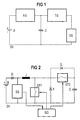
- a battery B is shown in FIG. 1, which generally delivers an output voltage in the range from 3.6 V to 5 V.
- the negative pole of the battery B is connected to a reference potential OV, for example.
- the output voltage of the battery B at its positive pole is stepped up to a voltage of, for example, 30 V in a step-up converter HS, and thus a capacitor C is charged.
- the step-up converter HS can be current-limited on the output side, so that the current supplied by the battery B pulsates only slightly. As a result, the battery B is only slightly loaded.
- the voltage applied to the capacitor C is transformed down to the supply voltage of the transmission voltage SS via a step-down converter TS.
- the voltage across the capacitor C drops to 10 V, for example.
- the basic principle of the invention is to step up the voltage on capacitor C, which acts as a buffer capacitor, compared to the output voltage of battery B, and then to lower the voltage on capacitor C to the required supply voltage of transmission stage SS.
- the capacitance of the capacitor C and thus also its size can be reduced.
- the supply voltage of the transmission stage SS can be selected largely independently of the output voltage of the battery B.
- the coil is the space-determining component that cannot be integrated.
- the step-up and step-down converter HS, TS were combined in such a way that a single coil I can be used for both switching regulators HS, TS.
- the battery B is in turn connected with its negative pole to the reference potential OV.
- the positive pole of the battery B is connected to the anode of a diode D.
- the transmitting stage SS is connected between the cathode of the diode D and the reference potential OV.
- the cathode of the diode D is further connected to one terminal of the coil I.
- the other connection of the coil I is connected to the reference potential OV via a switching element ST1.
- the other connection of the coil I is further connected via a switching element ST2 to a connection of the capacitor C, the other connection of which is connected to the reference potential OV.
- a free-wheeling diode F the anode of which is connected to the reference potential OV, can be connected in parallel with the switching element ST1.
- a rectifier diode G the cathode of which is connected to the capacitor C, can be connected in parallel with the switching element ST2.
- a control circuit SG is provided to control the switching elements ST1 and ST2.
- the control circuit SG is also connected to the transmission stage SS, for example, and receives the switch-on and switch-off times for the transmission bursts in the transmission mode of the transmission stage SS.
- the step-up converter HS shown in FIG. 1 is implemented in FIG. 2 by the coil I, the switching element ST1 and the rectifier diode G. Through this step-up converter HS, the output voltage output by battery B via diode D is stepped up and passed to capacitor C. During this operating phase, the switching element ST2 is in an open switching state, for example.
- the step-down converter TS shown in FIG. 1 is likewise implemented in FIG. 2 by the coil I, by the freewheeling diode F and the switching element ST2.
- the voltage which can be tapped off at the capacitor C is transformed down to the supply voltage by this step-down converter TS during the transmission operation of the transmission stage SS.
- the switching element ST1 is in an open switching state, for example.
- the supply voltage at the transmitter SS is in this combination of step-up and step-down converter HS, TS preferably approximately equal to or greater than the battery voltage.
- the switching elements are implemented by bidirectional switching transistors. MOS-FET components can be used for this.
- the freewheeling diode F and the rectifier diode G can be dispensed with. Their functions are realized by the corresponding control of the switching elements ST1 and ST2.
- the switching element ST1 is periodically switched on and off.
- the switching element ST2 is also switched on or off with the same period, the switching states of the two switching elements ST1 and ST2 being in opposite phases. This ensures that when the switching element ST1 is in the switching state, the switching element ST2 is in an open switching state and thus no current can flow out of the capacitor C.
- the switching element ST1 is in the open switching state, the switching element ST2 is in a conductive switching state and the current flows through the coil I to the capacitor C.
- the switching element ST2 of the buck converter TS is periodically switched on and off during the transmission operation of the transmission stage SS. With the same period, but in opposite phase, the switching element ST1 is also controlled.
- the switching element ST2 is in a conductive switching state, the switching element ST1 is in an open switching state and the current flows from the capacitor C through the coil I to the transmitting stage SS. If the switching element ST2 is in an open switching state, then the switching element ST1 is in a conductive switching state.
- This combination of the switching states of the switching elements ST1 and ST2 can have an effect the freewheeling diode F can be realized in the function as a buck converter TS.
- the battery power supply according to the invention can also be used to control display elements, for example light-emitting diodes or the like, in the radio or in general in a battery-powered terminal.
- the light yield of the light-emitting diodes can be improved by the invention, for example, as a result of the higher operating voltage.
- the starting behavior can be improved for the same reason.
Landscapes
- Engineering & Computer Science (AREA)
- Power Engineering (AREA)
- Charge And Discharge Circuits For Batteries Or The Like (AREA)
- Dc-Dc Converters (AREA)
Abstract
Description
- Die Erfindung bezieht sich auf eine Batterie-Stromversorgung gemäß dem Oberbegriff des Schutzanspruchs 1.
- Bei TDMA-(Time Division Multiple Access) Funksystemen sind die Funkgeräte nur für relativ kurze Zeit im Sendebetrieb, in dem sie einen sogenannten Sendeburst aussenden. Der pulsförmige Sendebetrieb bewirkt eine relativ hohe Stromaufnahme während des Sendeburst. Dies führt zu einer Verringerung der Lebensdauer der Batterie, so daß nur besonders geeignete Batterien für diese Funkgeräte verwendbar sind. Weiter ist die Strom- bzw. Spannungsversorgung für den höchsten vorkommenden Strom auszulegen, wobei Leitungs- und Schaltwiderstände ebenso wie die Innenwiderstände der Batterie sehr kritisch sind. Schließlich beeinflussen die pulsförmigen Versorgungsströme wahrend des Sendebetriebes auch umliegende Schaltungsteile, wie z.B. den NF-Verstärker und die Steuerung des Funkgerätes. Problematisch ist ferner, daß die Endstufen der Sendeeinrichtung des Funkgerätes nicht über den gesamten Betrieb der Versorgungsspannung mit ihrem optimalen Wirkungsgrad arbeiten, und meist an der unteren Grenze der Batteriespannung an ihrer Leistungsgrenze sind.
- Aus der europäischen Patentanmeldung 0 674 400 A1 ist eine Batterie-Stromversorgung für ein Funkgerät bekannt, wobei im Stromzuführungsweg eine Konstantstromquelle, sowie ein parallel zur Endstufe geschalteter Pufferkondensator angeordnet sind. Der Pufferkondensator wird mit einem Konstantstrom bis auf einen bestimmten Spannungswert aufgeladen. Während des Sendeburst im Sendebetrieb wird dieser Kondensator entladen und stellt den benötigten Strom für die Endstufen der Sendestufe zur Verfügung.
- Der Spannungsabfall während des Sendebursts muß sehr niedrig sein, in der Regel darf er sich nur im Bereich einiger hundert Millivolt bewegen. Es müssen daher für den Pufferkondensator sehr große Kapazitäten verwendet werden.
- Der Erfindung liegt die Aufgabe zugrunde, eine Batterie-Stromversorgung anzugeben, bei der der Kapazitätsbedarf für den Pufferkondensator reduziert ist.
- Diese Aufgabe wird erfindungsgemäß durch die im Schutzanspruch 1 angegebenen Merkmale gelöst.
- Durch die Kombination aus einem Hoch- und einem Tiefsetzsteller in der Batterie-Stromversorgung kann der Pufferkondensator in seiner Kapazität drastisch verkleinert werden. Damit ist auch der Platzbedarf für die Stromversorgung verringert.
- Bei der Ausgestaltung der Erfindung durch die gemeinsame Spule für Hoch- und Tiefsetzsteller kann der Platzbedarf weiter verringert werden.
- Im folgenden wird die Erfindung anhand eines in der Zeichnung dargestellten Ausführungsbeispieles beschrieben. Dabei zeigen:
- Figur 1
- das Blockschaltbild einer Schaltung zur Pufferung der Sendestufe und
- Figur 2
- ein Detailschaltbild dieser Schaltung.
- In Figur 1 ist eine Batterie B dargestellt, die in der Regel eine Ausgangsspannung im Bereich von 3,6 V bis 5 V abgibt. Der negative Pol der Batterie B ist beispielsweise mit einem Bezugspotential OV verbunden. Die Ausgangsspannung der Batterie B an ihrem Pluspol wird in einem Hochsetzsteller HS auf eine Spannung von beispielsweise 30 V hochtransformiert, und damit ein Kondensator C aufgeladen. Der Hochsetzsteller HS kann ausgangsseitig strombegrenzt sein, so daß der von der Batterie B gelieferte Strom nur wenig pulsiert. Hierdurch wird die Batterie B nur wenig belastet.
- Während des Sendebetriebes einer Sendestufe SS wird die am Kondensator C anliegende Spannung über einen Tiefsetzsteller TS auf die Versorgungsspannung der Sendespannung SS heruntertransformiert. Die Spannung am Kondensator C sinkt dabei auf beispielsweise 10 V ab.
- Das Grundprinzip der Erfindung besteht darin, die Spannung am Kondensator C, der als Pufferkondensator wirkt, gegenüber der Ausgangsspannung der Batterie B heraufzusetzen, und anschließend die Spannung am Kondensator C auf die benötigte Versorgungsspannug der Sendestufe SS herabzusetzen.
- Hierdurch kann die Kapazität des Kondensators C und damit auch dessen Baugröße verkleinert werden. Zudem ist bei dieser Stromversorgung der Sendestufe SS eines nicht näher dargestellte TDMA-Funkgerätes die Versorgungsspannung der Sendestufe SS weitgehend unabhängig wählbar von der Ausgangsspannung der Batterie B.
- Bei den Schaltreglern HS und TS ist jeweils die Spule das platzbestimmende, und nicht integrierbare Bauelement. Bei der in Figur 2 dargestellten Schaltung wurden der Hoch- und der Tiefsetzsteller HS, TS derart kombiniert, so daß für beide Schaltregler HS, TS eine einzige Spule I verwendet werden kann.
- Die Batterie B ist wiederum mit ihrem negativen Pol am Bezugspotential OV angeschaltet. Der positive Pol der Batterie B ist mit der Anode einer Diode D verbunden. Zwischen die Kathode der Diode D und das Bezugspotential OV ist die Sendestufe SS geschaltet.
- Die Kathode der Diode D ist weiter mit dem einen Anschluß der Spule I verbunden. Der andere Anschluß der Spule I ist über ein Schaltelement ST1 mit dem Bezugspotential OV verbunden. Der andere Anschluß der Spule I ist weiter über ein Schaltelement ST2 mit einem Anschluß des Kondensators C verbunden, dessen anderer Anschluß am Bezugspotential OV angeschaltet ist.
- Dem Schaltelement ST1 kann eine Freilaufdiode F parallelgeschaltet sein, deren Anode mit dem Bezugspotential OV verbunden ist. Dem Schaltelemente ST2 kann eine Gleichrichterdiode G parallel geschaltet sein, deren Kathode am Kondensator C angeschaltet ist.
- Zur Steuerung der Schaltelemente ST1 und ST2 ist eine Steuerschaltung SG vorgesehen. Die Steuerschaltung SG ist auch beispielsweise mit der Sendestufe SS verbunden, und erhält hierüber die Einschalt- und Ausschaltzeitpunkte für die Sendebursts im Sendebetrieb der Sendestufe SS.
- Der in Figur 1 dargestellte Hochsetzsteller HS wird in Figur 2 durch die Spule I, das Schaltelement ST1 und die Gleichrichterdiode G realisiert. Durch diesen Hochsetzsteller HS wird die von der Batterie B über die Diode D abgegebene Ausgangsspannung hochtransformiert und an den Kondensator C gegeben. Während dieser Betriebsphase ist beispielsweise das Schaltelement ST2 in einem offenen Schaltzustand.
- Der in Figur 1 dargestellte Tiefsetzsteller TS ist in Figur 2 ebenfalls durch die Spule I, durch die Freilaufdiode F und das Schaltelement ST2 realisiert. Die am Kondensator C abgreifbare Spannung wird während des Sendebetriebes der Sendestufe SS von diesem Tiefsetzsteller TS auf die Versorgungsspannung heruntertransformiert. Während dieser Betriebsphase ist das Schaltelemente ST1 beispielsweise in einem offenen Schaltzustand. Die Versorgungsspannung an der Sendestufe SS ist bei dieser Kombination aus Hoch- und Tiefsetzsteller HS, TS vorzugsweise in etwa gleich oder größer als die Batteriespannung.
- Bei einer bevorzugten Ausführungsform der Schaltung gemäß Figur 2 sind die Schaltelemente durch bidirektionale Schalttransistoren realisiert. Hierzu können MOS-FET-Bauelemente verwendet werden.
- Bei dieser Ausführungsform kann auf die Freilaufdiode F und die Gleichrichterdiode G verzichtet werden. Deren Funktionen werden durch die entsprechende Steuerung der Schaltelemente ST1 bzw. ST2 realisiert.
- Während des Aufladevorganges des Kondensators C durch den Hochsetzsteller HS wird das Schaltelemente ST1 periodisch ein- und ausgeschaltet. Gleichzeitig wird mit der gleichen Periode auch das Schaltelement ST2 ein- bzw. ausgeschaltet, wobei die Schaltzustände der beiden Schaltelemente ST1 und ST2 jeweils gegenphasig sind. Hierdurch ist sichergestellt, daß beim leitenden Schaltzustand des Schaltelementes ST1 das Schaltelement ST2 sich in einem offenen Schaltzustand befindet, und somit kein Strom vom Kondensator C abfließen kann. Beim offenen Schaltzustand des Schaltelementes ST1 ist das Schaltelement ST2 in einem leitenden Schaltzustand, und der Strom fließt durch die Spule I zum Kondensator C.
- Analog hierzu wird während des Sendebetriebes der Sendestufe SS das Schaltelement ST2 des Tiefsetzstellers TS periodisch ein- und ausgeschaltet. Mit der gleichen Periode, aber gegenphasig, wird auch das Schaltelement ST1 angesteuert. Bei einem leitenden Schaltzustand des Schaltelementes ST2 ist das Schaltelement ST1 in einem offenen Schaltzustand, und der Strom fließt vom Kondensator C durch die Spule I zur Sendestufe SS . Wenn sich das Schaltelement ST2 in einem offenen Schaltzustand befindet, dann ist das Schaltelement ST1 in einem leitenden Schaltzustand. Durch diese Kombination der Schaltzustände der Schaltelemente ST1 und ST2 kann die Wirkung der Freilaufdiode F bei der Funktion als Tiefsetzsteller TS realisiert werden.
- An Stelle der Sendeendstufe SS können mit der erfindungsgemäßen Batterie-Stromversorgung auch Anzeigeelemente, wie beispielsweise Leuchtdioden oder Ähnliches, im Funkgerät oder allgemein in einem batteriegespeisten Endgerät angesteuert werden. Durch die Erfindung kann beispielsweise die Lichtausbeute der Leuchtdioden in Folge der höheren Bertriebsspannung verbessert werden. Bei batteriebetriebenen Motoren beispielsweise kann aus dem gleichen Grund das Anlaufverhalten verbessert werden.
Claims (3)
- Batterie-Stromversorgung für eine Last (SS) mit periodischem, impulsartigem Strombedarf, insbesondere für ein TDMA-Funkgerät,
mit einer parallel zur Last (SS) geschalteten Kapazität (C) zur Pufferung,
gekennzeichnet durch einen Hochsetzsteller (HS) zur Aufladung der Kapazität (C), und
einen der Kapazität (C) nachgeschalteten Tiefsetzsteller (TS) zur Versorgung der Last (SS). - Batterie-Stromversorgung nach Anspruch 1,
gekennzeichnet durch eine gemeinsame Induktivität (I) für den Hochsetzsteller (HS) mit einem Schaltelement (ST1) und einer Gleichrichterdiode (G), und für den Tiefsetzsteller (TS) mit einem Schaltelement (ST2) und einer Freilaufdiode (F). - Batterie-Stromversorgung nach Anspruch 2,
gekennzeichnet durch bidirektionale, gegenphasig angesteuerte Schaltelemente in dem Hoch- und dem Tiefsetzsteller (HS, TS), wobei das Schaltelement (ST2) des Tiefsetzstellers (TS) die Gleichrichterdiode (G) für den Hochsetzsteller (HS), und das Schaltelement (ST1) des Hochsetzstellers (HS) die Freilaufdiode (F) für den Tiefsetzsteller (TS) realisiert.
Applications Claiming Priority (4)
| Application Number | Priority Date | Filing Date | Title |
|---|---|---|---|
| DE19612205 | 1996-03-27 | ||
| DE29605699U | 1996-03-27 | ||
| DE29605699U DE29605699U1 (de) | 1996-03-27 | 1996-03-27 | Batterie-Stromversorgung |
| DE19612205 | 1996-03-27 |
Publications (3)
| Publication Number | Publication Date |
|---|---|
| EP0798840A2 true EP0798840A2 (de) | 1997-10-01 |
| EP0798840A3 EP0798840A3 (de) | 1998-06-03 |
| EP0798840B1 EP0798840B1 (de) | 2002-01-30 |
Family
ID=26024203
Family Applications (1)
| Application Number | Title | Priority Date | Filing Date |
|---|---|---|---|
| EP97104065A Expired - Lifetime EP0798840B1 (de) | 1996-03-27 | 1997-03-11 | Batterie-Stromversorgung |
Country Status (2)
| Country | Link |
|---|---|
| EP (1) | EP0798840B1 (de) |
| DE (1) | DE59706207D1 (de) |
Cited By (5)
| Publication number | Priority date | Publication date | Assignee | Title |
|---|---|---|---|---|
| WO2001093411A1 (de) * | 2000-05-31 | 2001-12-06 | Siemens Ag Österreich | Pufferschaltung |
| DE102005030123A1 (de) * | 2005-06-28 | 2007-01-04 | Austriamicrosystems Ag | Stromversorgungsanordnung und deren Verwendung |
| EP1990924A1 (de) * | 2007-05-11 | 2008-11-12 | Actaris SAS | Batteriebetrieb für Radiofrequenzsender |
| US7768216B2 (en) | 2006-06-28 | 2010-08-03 | Austriamicrosystems Ag | Control circuit and method for controlling light emitting diodes |
| US8174209B2 (en) | 2008-01-30 | 2012-05-08 | Texas Instruments Deutschland Gmbh | DC-DC converter and method for minimizing battery peak pulse loading |
Family Cites Families (7)
| Publication number | Priority date | Publication date | Assignee | Title |
|---|---|---|---|---|
| JPS61144131A (ja) * | 1984-12-18 | 1986-07-01 | Toshiba Corp | バ−スト無線通信装置 |
| JPH04315320A (ja) * | 1991-04-15 | 1992-11-06 | Sony Corp | バースト無線通信装置 |
| ATE144663T1 (de) * | 1992-03-20 | 1996-11-15 | Siemens Ag | Schaltungsanordnung zur überbrückung von kurzzeitigen spannungsabfällen in batteriegespeisten funkgeräten |
| JPH05316646A (ja) * | 1992-05-07 | 1993-11-26 | Fujitsu Ltd | 電力供給回路 |
| JPH06252820A (ja) * | 1993-02-26 | 1994-09-09 | Sony Corp | 電源回路とそれを用いた無線通信装置 |
| US5423078A (en) * | 1993-03-18 | 1995-06-06 | Ericsson Ge Mobile Communications Inc. | Dual mode power amplifier for analog and digital cellular telephones |
| DE59506255D1 (de) * | 1994-03-24 | 1999-07-29 | Siemens Ag | Funkgerät |
-
1997
- 1997-03-11 EP EP97104065A patent/EP0798840B1/de not_active Expired - Lifetime
- 1997-03-11 DE DE59706207T patent/DE59706207D1/de not_active Expired - Fee Related
Cited By (9)
| Publication number | Priority date | Publication date | Assignee | Title |
|---|---|---|---|---|
| WO2001093411A1 (de) * | 2000-05-31 | 2001-12-06 | Siemens Ag Österreich | Pufferschaltung |
| US6801018B2 (en) | 2000-05-31 | 2004-10-05 | Siemens Ag Osterreich | Buffer circuit |
| DE102005030123A1 (de) * | 2005-06-28 | 2007-01-04 | Austriamicrosystems Ag | Stromversorgungsanordnung und deren Verwendung |
| WO2007000272A3 (de) * | 2005-06-28 | 2007-09-13 | Austriamicrosystems Ag | Stromversorgungsanordnung für einen led-blitz in einem mobiltelefon |
| US8716987B2 (en) | 2005-06-28 | 2014-05-06 | Ams Ag | Electrical power supply arrangement and use thereof |
| DE102005030123B4 (de) * | 2005-06-28 | 2017-08-31 | Austriamicrosystems Ag | Stromversorgungsanordnung und deren Verwendung |
| US7768216B2 (en) | 2006-06-28 | 2010-08-03 | Austriamicrosystems Ag | Control circuit and method for controlling light emitting diodes |
| EP1990924A1 (de) * | 2007-05-11 | 2008-11-12 | Actaris SAS | Batteriebetrieb für Radiofrequenzsender |
| US8174209B2 (en) | 2008-01-30 | 2012-05-08 | Texas Instruments Deutschland Gmbh | DC-DC converter and method for minimizing battery peak pulse loading |
Also Published As
| Publication number | Publication date |
|---|---|
| EP0798840A3 (de) | 1998-06-03 |
| DE59706207D1 (de) | 2002-03-14 |
| EP0798840B1 (de) | 2002-01-30 |
Similar Documents
| Publication | Publication Date | Title |
|---|---|---|
| DE112010005212B4 (de) | Dc/dc-spannungswandlervorrichtung | |
| EP1980012B9 (de) | Schaltungsanordnung zur spannungsversorgung und verfahren | |
| DE102008039351B3 (de) | Schaltungsanordnung zum Betrieb mindestens einer Halbleiterlichtquelle | |
| DE69508746T2 (de) | Selbstkonfigurierendes Batterieladegerät mit Mehrfachfunktionen als Versorgungsspannungsregler für batteriebetriebene Geräte | |
| DE102009041217A1 (de) | Spannungswandler und Verfahren zur Spannungswandlung | |
| DE19940419A1 (de) | Verfahren zum Betreiben von Aufwärts-Gleichspannungswandlern und Aufwärts-Gleichspannungswandler | |
| DE10030795B4 (de) | Gleichspannungswandlerschaltung | |
| DE19928309C2 (de) | Gleichspannungswandler | |
| DE10207138A1 (de) | Schaltung und Verfahren zum Verbessern des Wirkungsgrades eines Schaltreglers | |
| EP0573785B1 (de) | Stromversorgungsschaltung für ein Funkgerät | |
| DE60316392T2 (de) | Energierückgewinnungsschaltung und Stromwandlungssystem | |
| DE10328782B4 (de) | Steuerschaltung für einen MOSFET zur Synchrongleichrichtung | |
| DE102004060359A1 (de) | Laderegleranordnung und Verfahren zum Aufladen einer Batterie | |
| EP0798840B1 (de) | Batterie-Stromversorgung | |
| EP0201878A2 (de) | Schaltungsanordnung mit einem p-schaltenden n-Kanal MOS-Transistor | |
| DE29605699U1 (de) | Batterie-Stromversorgung | |
| EP1400007B1 (de) | Steuergerät für gleichstrommotoren mit kommutator | |
| EP0266743B1 (de) | Schaltungsanordnung zur Erzeugung einer internen Versorgungsspannung bei getakteten Stromversorgungen | |
| DE4007953C2 (de) | Gleichspannungswandler mit geschalteten Kondensatoren | |
| EP0404993B1 (de) | Gleichstromumrichter mit Strombegrenzung | |
| DE4203829C2 (de) | Gleichspannungs-Speiseschaltung | |
| EP1145913A2 (de) | Bordnetz mit Spannungsstabilisierung | |
| EP0027171A1 (de) | Durchfluss-Gleichstromumrichter | |
| DE3927734C2 (de) | ||
| WO2008074666A1 (de) | Spannungskonverter und verfahren zur spannungsvervielfachung |
Legal Events
| Date | Code | Title | Description |
|---|---|---|---|
| PUAI | Public reference made under article 153(3) epc to a published international application that has entered the european phase |
Free format text: ORIGINAL CODE: 0009012 |
|
| AK | Designated contracting states |
Kind code of ref document: A2 Designated state(s): DE FI FR GB IT SE |
|
| PUAL | Search report despatched |
Free format text: ORIGINAL CODE: 0009013 |
|
| AK | Designated contracting states |
Kind code of ref document: A3 Designated state(s): DE FI FR GB IT SE |
|
| 17P | Request for examination filed |
Effective date: 19980707 |
|
| 17Q | First examination report despatched |
Effective date: 19991108 |
|
| GRAG | Despatch of communication of intention to grant |
Free format text: ORIGINAL CODE: EPIDOS AGRA |
|
| GRAG | Despatch of communication of intention to grant |
Free format text: ORIGINAL CODE: EPIDOS AGRA |
|
| GRAH | Despatch of communication of intention to grant a patent |
Free format text: ORIGINAL CODE: EPIDOS IGRA |
|
| GRAH | Despatch of communication of intention to grant a patent |
Free format text: ORIGINAL CODE: EPIDOS IGRA |
|
| GRAA | (expected) grant |
Free format text: ORIGINAL CODE: 0009210 |
|
| REG | Reference to a national code |
Ref country code: GB Ref legal event code: IF02 |
|
| AK | Designated contracting states |
Kind code of ref document: B1 Designated state(s): DE FI FR GB IT SE |
|
| PG25 | Lapsed in a contracting state [announced via postgrant information from national office to epo] |
Ref country code: FI Free format text: LAPSE BECAUSE OF FAILURE TO SUBMIT A TRANSLATION OF THE DESCRIPTION OR TO PAY THE FEE WITHIN THE PRESCRIBED TIME-LIMIT Effective date: 20020130 |
|
| REF | Corresponds to: |
Ref document number: 59706207 Country of ref document: DE Date of ref document: 20020314 |
|
| PG25 | Lapsed in a contracting state [announced via postgrant information from national office to epo] |
Ref country code: SE Free format text: LAPSE BECAUSE OF FAILURE TO SUBMIT A TRANSLATION OF THE DESCRIPTION OR TO PAY THE FEE WITHIN THE PRESCRIBED TIME-LIMIT Effective date: 20020430 |
|
| GBT | Gb: translation of ep patent filed (gb section 77(6)(a)/1977) |
Effective date: 20020409 |
|
| ET | Fr: translation filed | ||
| PLBE | No opposition filed within time limit |
Free format text: ORIGINAL CODE: 0009261 |
|
| STAA | Information on the status of an ep patent application or granted ep patent |
Free format text: STATUS: NO OPPOSITION FILED WITHIN TIME LIMIT |
|
| 26N | No opposition filed | ||
| PGFP | Annual fee paid to national office [announced via postgrant information from national office to epo] |
Ref country code: FR Payment date: 20060324 Year of fee payment: 10 |
|
| PGFP | Annual fee paid to national office [announced via postgrant information from national office to epo] |
Ref country code: DE Payment date: 20060522 Year of fee payment: 10 |
|
| REG | Reference to a national code |
Ref country code: GB Ref legal event code: 732E |
|
| REG | Reference to a national code |
Ref country code: FR Ref legal event code: TP |
|
| GBPC | Gb: european patent ceased through non-payment of renewal fee |
Effective date: 20070311 |
|
| PGFP | Annual fee paid to national office [announced via postgrant information from national office to epo] |
Ref country code: IT Payment date: 20070524 Year of fee payment: 11 |
|
| REG | Reference to a national code |
Ref country code: FR Ref legal event code: ST Effective date: 20071130 |
|
| PG25 | Lapsed in a contracting state [announced via postgrant information from national office to epo] |
Ref country code: DE Free format text: LAPSE BECAUSE OF NON-PAYMENT OF DUE FEES Effective date: 20071002 |
|
| PG25 | Lapsed in a contracting state [announced via postgrant information from national office to epo] |
Ref country code: GB Free format text: LAPSE BECAUSE OF NON-PAYMENT OF DUE FEES Effective date: 20070311 |
|
| PG25 | Lapsed in a contracting state [announced via postgrant information from national office to epo] |
Ref country code: FR Free format text: LAPSE BECAUSE OF NON-PAYMENT OF DUE FEES Effective date: 20070402 |
|
| PGFP | Annual fee paid to national office [announced via postgrant information from national office to epo] |
Ref country code: GB Payment date: 20060308 Year of fee payment: 10 |
|
| PG25 | Lapsed in a contracting state [announced via postgrant information from national office to epo] |
Ref country code: IT Free format text: LAPSE BECAUSE OF NON-PAYMENT OF DUE FEES Effective date: 20080311 |