EP0800139A2 - Programmierbares Lese/-Schreibzugriffsignal und Verfahren - Google Patents
Programmierbares Lese/-Schreibzugriffsignal und Verfahren Download PDFInfo
- Publication number
- EP0800139A2 EP0800139A2 EP97104658A EP97104658A EP0800139A2 EP 0800139 A2 EP0800139 A2 EP 0800139A2 EP 97104658 A EP97104658 A EP 97104658A EP 97104658 A EP97104658 A EP 97104658A EP 0800139 A2 EP0800139 A2 EP 0800139A2
- Authority
- EP
- European Patent Office
- Prior art keywords
- read
- write access
- processor
- address space
- external device
- Prior art date
- Legal status (The legal status is an assumption and is not a legal conclusion. Google has not performed a legal analysis and makes no representation as to the accuracy of the status listed.)
- Withdrawn
Links
Images
Classifications
-
- G—PHYSICS
- G06—COMPUTING OR CALCULATING; COUNTING
- G06F—ELECTRIC DIGITAL DATA PROCESSING
- G06F13/00—Interconnection of, or transfer of information or other signals between, memories, input/output devices or central processing units
- G06F13/14—Handling requests for interconnection or transfer
- G06F13/16—Handling requests for interconnection or transfer for access to memory bus
- G06F13/1668—Details of memory controller
- G06F13/1694—Configuration of memory controller to different memory types
-
- G—PHYSICS
- G06—COMPUTING OR CALCULATING; COUNTING
- G06F—ELECTRIC DIGITAL DATA PROCESSING
- G06F13/00—Interconnection of, or transfer of information or other signals between, memories, input/output devices or central processing units
- G06F13/38—Information transfer, e.g. on bus
- G06F13/42—Bus transfer protocol, e.g. handshake; Synchronisation
- G06F13/4204—Bus transfer protocol, e.g. handshake; Synchronisation on a parallel bus
- G06F13/4208—Bus transfer protocol, e.g. handshake; Synchronisation on a parallel bus being a system bus, e.g. VME bus, Futurebus, Multibus
Definitions
- the present invention relates in general to data processing systems, and in particular, to a programmable read/write access signal delivered from a processor.
- a processor (hereinafter also referred to as a CPU (central processing unit)) is typically implemented on an integrated circuit ("IC") and is coupled to various external resources (devices) by a system bus.
- external devices may include flash memory devices, read-only memory (“ROM”) devices, random access memory (“RAM”) devices, dynamic random access memory (“DRAM”) devices, universal asynchronous receiver/transmitter (“UART”) devices, application specific integrated circuits (“ASIC”), timer devices, other microprocessors, direct memory access (“DMA”) channels, hard disks, tape drives, CD-ROMs, network communications adapters, user interfaces, and display devices.
- ROM read-only memory
- RAM random access memory
- DRAM dynamic random access memory
- UART universal asynchronous receiver/transmitter
- ASIC application specific integrated circuits
- timer devices other microprocessors, direct memory access (“DMA”) channels, hard disks, tape drives, CD-ROMs, network communications adapters, user interfaces, and display devices.
- DMA direct memory access
- the system bus which couples all of these various external devices to the processor, is typically a plurality of transmission lines operating in parallel. It could be said that the equivalent of the bus in the human body is the central nervous system.
- an addressing scheme is needed so that only the intended destination of a set of data or instructions transmitted from the processor or from one of the external devices is received by that intended destination.
- the set of addresses for a particular system can be parsed into a plurality of address spaces.
- An address space is made up of one or more addresses.
- a particular address space may be dedicated to a particular external device.
- the address spaces are generally indicated by asserting a chip select signal to a specific device.
- a bus protocol is initiated between the processor and the external device corresponding to the particular address space.
- This bus protocol typically includes an alert signal to the external device that a read or write access is about to occur, and a notification to the external device to indicate whether or not the access is a read or a write.
- This bus protocol is produced by a system bus controller located in the processor and is coupled between the core circuitry of the processor (hereinafter referred to also as the "core") and the system bus.
- the system bus controller acts as an interface between read and write requests received from the core and the system bus.
- different types of external memory devices may require differing values of read/write access signals in order to interface correctly with the processor.
- Prior art processors are rigid in that they produce only one value for the read/write access signal. If this signal is asserted high by the processor for a write access to an external device, but the external device requires that this received signal be asserted low, then the processor and the external device will not be able to interface correctly.
- the external device may operate as if the write access from the processor is a read access.
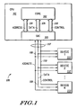
- processor 101 is coupled to N (where N is a positive integer) external devices 111-113 by system bus 107, which is a "glueless" interface.
- system bus 107 which is a "glueless" interface.
- external logic circuitry is not required to be implemented anywhere along system bus 107 in order that CPU 101 can properly interface with each of the N external devices 111-113.
- CPU 101 includes processor core 102, which typically comprises various execution units and related circuitry.
- Core 102 is coupled to system bus controller ("SBC") 103 by address bus 104, data bus 105, and control bus 106.
- SBC 103 operates as a bus interface unit between core 102 and system bus 107.
- System bus 107 includes address bus 108, data bus 109, and control bus 110. System bus 107 couples CPU 101 to each of the N external devices 111-113.
- each of the N external devices 111-113 resides in an address space to which read and write accesses may be conducted.
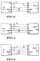
- FIG. 2 there is illustrated a coupling of CPU 101 to external device 111.
- a portion of control bus 110 is illustrated in more detail to show the unique requirement by external device 111 for control signals for interfacing CPU 101 and external device 111.
- External device 111 requires that the read/write access signal, labeled as ERE, from CPU 101 is received by the output enable (OE) and write enable (WE) pins of external device 111.
- the chip select (CS) signal of CPU 101 is received by the chip enable (CE) pin of external device 111.
- FIG. 3 illustrates a coupling of CPU 101 to external device 112, which is a different external device than external device 111.
- External device 112 requires that the ERE signal from CPU 101 be received only by the OE pin of external device 112.
- the WE pin of external device 112 is coupled to the WE pin of CPU 101.
- FIG. 4 illustrates yet another example of a coupling of CPU 101 to an external device different than external devices 111 and 112.
- External device 113 has its OE pin tied to ground, and the WE pin of external device 113 receives the ERE signal from CPU 101.
- External devices 111-113 may comprise different memory devices such as SRAM, ROM or flash memory chips. Such different memory chips often require different control interfaces in order to communicate with a processor with respect to read and write accesses. For example, for a write access from CPU 101, external device 112 may require that the ERE signal be asserted low, while external device 113 may require that, for a write access, the ERE signal be asserted high. As discussed above, prior art processors are rigidly configured so that, for any access (read or write), the ERE signal is always asserted at the same level. For example, in a prior art processor, for a write access, the ERE signal may always be asserted low.
- an external logic circuit such as an inverter circuit
- the present invention solves the foregoing problem without requiring such additional external logic circuitry.
- a "glueless" interface can be implemented between CPU 101 and all of external devices 111-113.
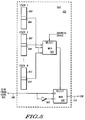
- SBC 103 receives a read or write access (labeled R/W) from core 102 on control bus 106.
- core 102 may request that it be able to write information to an address space, corresponding to an address received by SBC 103 on address bus 104 (see FIG. 1), to one of external devices 111-113, corresponding to the address space.
- Such a write access from core 102 on bus 106 could be implemented as an asserted-high or an asserted-low signal. This signal is received by the "0" input of multiplexer circuit (mux) 502 within SBC 103.
- multiplexer circuit (mux) 502 is received by the "0" input of multiplexer circuit (mux) 502 within SBC 103.
- This write access signal is also inverted by inverter 503, which has its output coupled to the "1" input of mux 502. Selection of either one of these inputs to be output as the ERE signal from SBC 103 is performed as a function of a register value within one of bits 604, 608, or 612 in registers 603, 607, or 611, respectively.
- Registers 603, 607, and 611 may each be a chip select control register (CSCR) implemented within SBC 103. Bit values within a CSCR define the external bus control signals for an external device for a given address space. Selection of one of bits 604, 608, or 612 is made by multiplexer circuit 510 as a function of the specified address space of the read or write access from core 102.
- Each of registers 603, 607 and 611 is dedicated to a different address space within system 100.
- bits 604, 608, and 612 (which each may be comprised of one or more bits) have been preprogrammed into registers 603, 607, and 611, respectively, at the time data processing system 100 is configured by the program executing on CPU 101.
- a system engineer may purchase CPU 101 configured in accordance with the present invention for coupling within system 100 to one or more of external devices 111-113.
- the system engineer will take note of the particular read/write access protocol requirements of the various external devices 111-113 and will generate the appropriate program instructions to configure the required values within each of bits 604, 608, and 612 pertaining to each of external devices 111-113, respectively, so that SBC 103 produces the required ERE signal value levels needed by each of the external devices (address spaces).
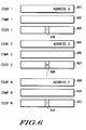
- each address space will have a dedicated set of chip select registers (see FIG. 6). Note that one skilled in the art will be able to perform this preprogramming feature. Alternatively, programming of bits 604, 608, and/or 612 may occur during a reset of the integrated circuit.
- chip select registers 601-603 are dedicated to external device 111
- chip select registers 605-607 are dedicated to external device 112
- chip select registers 609-611 are dedicated to external device 113. Therefore, when an address indicates one of external devices 111, 112 or 113 should be accessed, a set of chip select registers corresponding to the selected one of the external devices will provide control information during that access.
- Registers 601, 605, and 609 may be typical chip select address registers for storing the address pertaining to a particular read or write access received from core 102.
- Registers 602, 606, and 610 may be optional mask registers used in combination with the chip select address registers for defining address spaces within data processing system 100. And, as noted previously, registers 603, 607, and 611 are chip select control registers for containing various control bits for directing the particular control signals to be sent to their respective external devices.
- register bits 604, 608, and 612 are the ERE bits used within their respective CSCR registers for determining the required ERE signal to be sent to the corresponding external device.
- mux 502 may receive the register value in bit 604 for determining the signal level of the ERE signal to be sent to external device 111.
- the table shown below illustrates an example of how these ERE bits are programmed for proper operation of read and write accesses from CPU 101 to external devices 111-113 as shown in FIGS. 2, 3 and 4.
- ERE bit value is a "0"
- the ERE signal output will be asserted low for a write access and asserted high for a read access. If the ERE bit value is a 1, then a read access will result in an ERE signal asserted low, while a write access will result in an ERE signal asserted high.
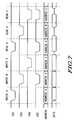
- FIG. 7 An example of this is further illustrated in FIG. 7 by the timing diagram, which illustrates three consecutive write accesses and three consecutive read accesses requested by core 102. In the first write access, a write access is to occur to address space A. Address A is stored within register 601. This will cause a chip select signal (CS1) to be sent from SBC 103 to external device 111.
- CS1 chip select signal
- mux 502 Since the register value within bit 604 of register 603 is a "1" bit, mux 502 will select the "1" input, which is the inverted signal of the write access signal received from core 102. Therefore, the ERE signal sent to external device 111 will be asserted high.
- the chip select signal CS2 When the write access to address B is received, the chip select signal CS2 will be asserted low and sent to external device 112. Since the register value within bit 608 is a "0" bit, the ERE signal sent from SBC 103 to external device 112 will be asserted low.
- chip select signal CSN When the write access from core 102 is received and intended for address C, which corresponds to external device 113, chip select signal CSN will be asserted low and sent to external device 113. Since the register value within bit 612 is a "1" bit, the ERE signal sent from SBC 103 to external device 113 will be asserted high.
- the value for the ERE signal is opposite for the read accesses as it was for the write accesses for the same set of addresses.
- An advantage of the present invention is that the ERE signal sent from SBC 103 to the various external devices 111-113 is programmable so that external logic circuitry is not required in order to modify this ERE signal before being received by each of external devices 111-113, which may have differing requirements for the level of this ERE signal.
Landscapes
- Engineering & Computer Science (AREA)
- Theoretical Computer Science (AREA)
- Physics & Mathematics (AREA)
- General Engineering & Computer Science (AREA)
- General Physics & Mathematics (AREA)
- Microcomputers (AREA)
- Multi Processors (AREA)
- Bus Control (AREA)
Applications Claiming Priority (2)
| Application Number | Priority Date | Filing Date | Title |
|---|---|---|---|
| US627669 | 1996-04-01 | ||
| US08/627,669 US5872940A (en) | 1996-04-01 | 1996-04-01 | Programmable read/write access signal and method therefor |
Publications (2)
| Publication Number | Publication Date |
|---|---|
| EP0800139A2 true EP0800139A2 (de) | 1997-10-08 |
| EP0800139A3 EP0800139A3 (de) | 1999-03-10 |
Family
ID=24515604
Family Applications (1)
| Application Number | Title | Priority Date | Filing Date |
|---|---|---|---|
| EP97104658A Withdrawn EP0800139A3 (de) | 1996-04-01 | 1997-03-19 | Programmierbares Lese/-Schreibzugriffsignal und Verfahren |
Country Status (9)
| Country | Link |
|---|---|
| US (1) | US5872940A (de) |
| EP (1) | EP0800139A3 (de) |
| JP (1) | JPH1055331A (de) |
| KR (1) | KR970071302A (de) |
| CN (1) | CN1171577A (de) |
| IE (1) | IE970147A1 (de) |
| IL (1) | IL120309A0 (de) |
| SG (1) | SG64973A1 (de) |
| TW (1) | TW337564B (de) |
Cited By (1)
| Publication number | Priority date | Publication date | Assignee | Title |
|---|---|---|---|---|
| EP1069506A1 (de) * | 1999-07-09 | 2001-01-17 | Princeton Technology Corporation | Ein paralleles Bussystem mit Peripheriegeräteerweiterungsfähigkeit |
Families Citing this family (13)
| Publication number | Priority date | Publication date | Assignee | Title |
|---|---|---|---|---|
| JP3304895B2 (ja) * | 1998-10-08 | 2002-07-22 | 日本電気株式会社 | 補助記録装置の接続方法およびその装置 |
| US6725307B1 (en) * | 1999-09-23 | 2004-04-20 | International Business Machines Corporation | Method and system for controlling data transfers with physical separation of data functionality from address and control functionality in a distributed multi-bus multiprocessor system |
| US7529799B2 (en) * | 1999-11-08 | 2009-05-05 | International Business Machines Corporation | Method and apparatus for transaction tag assignment and maintenance in a distributed symmetric multiprocessor system |
| JP3663106B2 (ja) * | 2000-02-28 | 2005-06-22 | 東芝機械株式会社 | データ入出力装置 |
| JP2003015790A (ja) * | 2001-06-28 | 2003-01-17 | Oki Electric Ind Co Ltd | 半導体集積回路 |
| US7162554B1 (en) * | 2001-07-11 | 2007-01-09 | Advanced Micro Devices, Inc. | Method and apparatus for configuring a peripheral bus |
| EP1286270A1 (de) * | 2001-07-24 | 2003-02-26 | Deutsche Thomson-Brandt Gmbh | Integrierte Schaltung mit generischer Kommunikationsschnittstelle |
| US6876563B1 (en) * | 2002-12-20 | 2005-04-05 | Cypress Semiconductor Corporation | Method for configuring chip selects in memories |
| US7610061B2 (en) * | 2003-09-20 | 2009-10-27 | Samsung Electronics Co., Ltd. | Communication device and method having a common platform |
| CN1307571C (zh) * | 2004-11-26 | 2007-03-28 | 上海广电(集团)有限公司中央研究院 | 一种低速总线结构及其数据传输方法 |
| US7702839B2 (en) * | 2005-04-12 | 2010-04-20 | Nokia Corporation | Memory interface for volatile and non-volatile memory devices |
| US10120829B2 (en) | 2016-11-23 | 2018-11-06 | Infineon Technologies Austria Ag | Bus device with programmable address |
| CN110781118B (zh) * | 2019-09-30 | 2023-11-03 | 深圳震有科技股份有限公司 | 实现并行总线从模式的方法及装置、计算机设备、介质 |
Family Cites Families (11)
| Publication number | Priority date | Publication date | Assignee | Title |
|---|---|---|---|---|
| US5325513A (en) * | 1987-02-23 | 1994-06-28 | Kabushiki Kaisha Toshiba | Apparatus for selectively accessing different memory types by storing memory correlation information in preprocessing mode and using the information in processing mode |
| US4933845A (en) * | 1987-09-04 | 1990-06-12 | Digital Equipment Corporation | Reconfigurable bus |
| US5265243A (en) * | 1989-03-27 | 1993-11-23 | Motorola, Inc. | Processor interface controller for interfacing peripheral devices to a processor |
| US5448744A (en) * | 1989-11-06 | 1995-09-05 | Motorola, Inc. | Integrated circuit microprocessor with programmable chip select logic |
| IL96808A (en) * | 1990-04-18 | 1996-03-31 | Rambus Inc | Introductory / Origin Circuit Agreed Using High-Performance Brokerage |
| KR0181471B1 (ko) * | 1990-07-27 | 1999-05-15 | 윌리암 피.브레이든 | 컴퓨터 데이타 경로배정 시스템 |
| JPH04163655A (ja) * | 1990-10-26 | 1992-06-09 | Mitsubishi Electric Corp | 入出力装置 |
| US5557757A (en) * | 1994-02-02 | 1996-09-17 | Advanced Micro Devices | High performance integrated processor architecture including a sub-bus control unit for generating signals to control a secondary, non-multiplexed external bus |
| US5721860A (en) * | 1994-05-24 | 1998-02-24 | Intel Corporation | Memory controller for independently supporting synchronous and asynchronous DRAM memories |
| US5535349A (en) * | 1994-06-09 | 1996-07-09 | Motorola, Inc. | Data processing system and method for providing chip selects to peripheral devices |
| EP0691616A1 (de) * | 1994-07-08 | 1996-01-10 | Advanced Micro Devices, Inc. | RAM-/ und ROM-Steuerungseinheit |
-
1996
- 1996-04-01 US US08/627,669 patent/US5872940A/en not_active Expired - Fee Related
-
1997
- 1997-02-25 IL IL12030997A patent/IL120309A0/xx unknown
- 1997-02-27 TW TW086102417A patent/TW337564B/zh active
- 1997-03-03 IE IE970147A patent/IE970147A1/en not_active IP Right Cessation
- 1997-03-19 EP EP97104658A patent/EP0800139A3/de not_active Withdrawn
- 1997-03-19 SG SG1997000848A patent/SG64973A1/en unknown
- 1997-03-28 JP JP9094570A patent/JPH1055331A/ja active Pending
- 1997-03-28 CN CN97109921A patent/CN1171577A/zh active Pending
- 1997-04-01 KR KR1019970012616A patent/KR970071302A/ko not_active Withdrawn
Cited By (1)
| Publication number | Priority date | Publication date | Assignee | Title |
|---|---|---|---|---|
| EP1069506A1 (de) * | 1999-07-09 | 2001-01-17 | Princeton Technology Corporation | Ein paralleles Bussystem mit Peripheriegeräteerweiterungsfähigkeit |
Also Published As
| Publication number | Publication date |
|---|---|
| US5872940A (en) | 1999-02-16 |
| SG64973A1 (en) | 1999-05-25 |
| IE970147A1 (en) | 1997-10-08 |
| TW337564B (en) | 1998-08-01 |
| IL120309A0 (en) | 1997-06-10 |
| CN1171577A (zh) | 1998-01-28 |
| KR970071302A (ko) | 1997-11-07 |
| JPH1055331A (ja) | 1998-02-24 |
| EP0800139A3 (de) | 1999-03-10 |
Similar Documents
| Publication | Publication Date | Title |
|---|---|---|
| US6701405B1 (en) | DMA handshake protocol | |
| US10270447B2 (en) | Apparatus for configurable interface and associated methods | |
| US5872940A (en) | Programmable read/write access signal and method therefor | |
| US5978865A (en) | System for performing DMA transfers where an interrupt request signal is generated based on the value of the last of a plurality of data bits transmitted | |
| JPS59168556A (ja) | 集積回路マイクロプロセツサ | |
| US20050108454A1 (en) | Method and apparatus for providing an inter integrated circuit interface with an expanded address range and efficient priority-based data throughput | |
| US5574869A (en) | Bus bridge circuit having configuration space enable register for controlling transition between various modes by writing the bridge identifier into CSE register | |
| US5416916A (en) | Structure for enabling direct memory-to-memory transfer with a fly-by DMA unit | |
| US5896549A (en) | System for selecting between internal and external DMA request where ASP generates internal request is determined by at least one bit position within configuration register | |
| US5535419A (en) | Sytem and method for merging disk change data from a floppy disk controller with data relating to an IDE drive controller | |
| US6754760B1 (en) | Programmable interface for a configurable system bus | |
| US20040230754A1 (en) | Memory system for a radiotelephone | |
| US7062588B2 (en) | Data processing device accessing a memory in response to a request made by an external bus master | |
| JPS63116258A (ja) | デ−タ処理システム | |
| US7043592B2 (en) | External bus controller | |
| EP0321775B1 (de) | Sicheres Datenverarbeitungssystem, das Artikelbausteine benutzt | |
| JPS6246025B2 (de) | ||
| US20060090024A1 (en) | Bus controller | |
| EP0691616A1 (de) | RAM-/ und ROM-Steuerungseinheit | |
| CA1252573A (en) | Dual bus system | |
| JPS6242306B2 (de) | ||
| KR0165505B1 (ko) | 공유메모리를 사용한 통신장치 | |
| JPH02207363A (ja) | データ転送制御方式、デバイスコントローラ、およびメモリ・コントローラ | |
| KR100236330B1 (ko) | 피씨아이(PCI) 슬레이브(Slave) 어드레스 스테핑(Spepping)장치 | |
| KR100452332B1 (ko) | 데이터 읽기 및 쓰기 속도 개선 방법 |
Legal Events
| Date | Code | Title | Description |
|---|---|---|---|
| PUAI | Public reference made under article 153(3) epc to a published international application that has entered the european phase |
Free format text: ORIGINAL CODE: 0009012 |
|
| AK | Designated contracting states |
Kind code of ref document: A2 Designated state(s): DE GB |
|
| PUAL | Search report despatched |
Free format text: ORIGINAL CODE: 0009013 |
|
| AK | Designated contracting states |
Kind code of ref document: A3 Designated state(s): DE GB |
|
| STAA | Information on the status of an ep patent application or granted ep patent |
Free format text: STATUS: THE APPLICATION IS DEEMED TO BE WITHDRAWN |
|
| 18D | Application deemed to be withdrawn |
Effective date: 19990911 |