EP0800317A2 - Farbkamera mit einem einzigen CCD-Farbbildsensor mit höherer Auflösung, der fähig ist, Geisterfarberzeugung zu begrenzen - Google Patents
Farbkamera mit einem einzigen CCD-Farbbildsensor mit höherer Auflösung, der fähig ist, Geisterfarberzeugung zu begrenzen Download PDFInfo
- Publication number
- EP0800317A2 EP0800317A2 EP97105161A EP97105161A EP0800317A2 EP 0800317 A2 EP0800317 A2 EP 0800317A2 EP 97105161 A EP97105161 A EP 97105161A EP 97105161 A EP97105161 A EP 97105161A EP 0800317 A2 EP0800317 A2 EP 0800317A2
- Authority
- EP
- European Patent Office
- Prior art keywords
- color
- signal
- pixels
- rows
- filters
- Prior art date
- Legal status (The legal status is an assumption and is not a legal conclusion. Google has not performed a legal analysis and makes no representation as to the accuracy of the status listed.)
- Granted
Links
Images








Classifications
-
- H—ELECTRICITY
- H10—SEMICONDUCTOR DEVICES; ELECTRIC SOLID-STATE DEVICES NOT OTHERWISE PROVIDED FOR
- H10D—INORGANIC ELECTRIC SEMICONDUCTOR DEVICES
- H10D48/00—Individual devices not covered by groups H10D1/00 - H10D44/00
- H10D48/30—Devices controlled by electric currents or voltages
- H10D48/32—Devices controlled by only the electric current supplied, or only the electric potential applied, to an electrode which does not carry the current to be rectified, amplified or switched
- H10D48/36—Unipolar devices
-
- H—ELECTRICITY
- H04—ELECTRIC COMMUNICATION TECHNIQUE
- H04N—PICTORIAL COMMUNICATION, e.g. TELEVISION
- H04N25/00—Circuitry of solid-state image sensors [SSIS]; Control thereof
- H04N25/40—Extracting pixel data from image sensors by controlling scanning circuits, e.g. by modifying the number of pixels sampled or to be sampled
- H04N25/44—Extracting pixel data from image sensors by controlling scanning circuits, e.g. by modifying the number of pixels sampled or to be sampled by partially reading an SSIS array
- H04N25/447—Extracting pixel data from image sensors by controlling scanning circuits, e.g. by modifying the number of pixels sampled or to be sampled by partially reading an SSIS array by preserving the colour pattern with or without loss of information
-
- H—ELECTRICITY
- H04—ELECTRIC COMMUNICATION TECHNIQUE
- H04N—PICTORIAL COMMUNICATION, e.g. TELEVISION
- H04N25/00—Circuitry of solid-state image sensors [SSIS]; Control thereof
- H04N25/10—Circuitry of solid-state image sensors [SSIS]; Control thereof for transforming different wavelengths into image signals
- H04N25/11—Arrangement of colour filter arrays [CFA]; Filter mosaics
- H04N25/13—Arrangement of colour filter arrays [CFA]; Filter mosaics characterised by the spectral characteristics of the filter elements
- H04N25/135—Arrangement of colour filter arrays [CFA]; Filter mosaics characterised by the spectral characteristics of the filter elements based on four or more different wavelength filter elements
- H04N25/136—Arrangement of colour filter arrays [CFA]; Filter mosaics characterised by the spectral characteristics of the filter elements based on four or more different wavelength filter elements using complementary colours
Definitions
- the present invention relates generally to color cameras, and more particularly to a single CCD type color camera having a color separation circuit for processing a signal from a solid state imaging device which includes photoelectric conversion elements arranged in an array corresponding to color filters arranged in a color differentially ordered array, and a method of separating color signals using such a circuit.
- a CCD Charge Coupled Device
- a CCD Charge Coupled Device which is widely used today as an imaging device in a color camera simply changes the amplitude of a signal to output in response to the brightness of light which it receives, and the output signal does not include any color information. Therefore, in order to obtain color information, some optical means must be employed for example for filtering light incident to the CCD.
- a so-called single CCD type color camera which extracts three primary color signals from a single CCD is employed, and a color filter array is used on the side of the light receiving surface of the CCD according to a so-called simultaneous color imaging method.
- Fig. 16 is a block diagram schematically showing the structure of an inter-line transfer CCD 10 generally used in a color camera for home use.
- Inter-line transfer CCD 10 includes a photosensitive portion 12 formed of pn junction type photodiodes arranged in an array, a transfer portion 14 including an analog shift register formed of a CCD, and a horizontal transfer register 16 for transferring signals formed by converting signal charges sequentially transferred from transfer portion 14 into voltage in the horizontal direction for output.
- Fig. 16 includes pn junction type photodiodes corresponding to three pixels arranged each in the vertical and horizontal direction for ease of illustration.
- photodiodes corresponding to 500 pixels in the vertical direction and 500 to 800 pixels in the horizontal direction are arranged in an array.
- the inter-line transfer CCD is generally driven in two modes, i.e., frame accumulation and field accumulation.
- the field accumulation mode used corresponding to a color differentially ordered color filter array will be detailed.
- Figs. 17A and 17B are schematic diagrams for use in illustration of how signal charges are read out form inter-line transfer CCD 10 according to the field accumulation mode
- Fig. 17A shows a method of reading out a signal charge in an odd-numbered field
- Fig. 17B a method of reading out a signal charge in an even-numbered field.
- signals from an odd-numbered pixel and an even-numbered pixel in the vertical direction are simultaneously transferred from the photosensitive portion to the transfer portion, where the signals are added.
- color differential signals are separated using such a method of transferring in inter-line transfer CCD 10.
- Fig. 18 is a diagram schematically showing the flow of processing a signal output from inter-line transfer CCD 10 when the color filter array is color differentially ordered.
- color filters of magenta hereinafter Mg
- green hereinafter G
- cyan hereinafter Cy
- Ye yellow
- Mg, G, Ye and Cy described above as the colors of color filters permits the intensity of a G signal weighing the most in a luminance signal among three primary colors R, G and B to be higher than that of a B signal.
- color filters of Ye and color filters of Cy are alternately arranged in the horizontal direction.
- the method of reading out from inter-line transfer CCD 10 having the color filter array arrangement is on the basis of 2-pixel addition reading in the vertical direction (y-direction).
- an odd-numbered pixel and an even-numbered pixel in the vertical direction are added, and in the following even-numbered field, a different combination of an even-numbered pixel and an odd-numbered pixel are added.
- signals are output in the order of G+Cy, Mg+Ye, ... in the n-th scanning line and in the order of Mg+Cy, G+Ye, ... in the n+1-th scanning line.
- These signals are pulse amplitude modulated signals as shown in Fig. 18.
- the complementary color signals are replaced by three primary color signals and indicated as the amplitude modulated waveforms of the three primary color signals.
- a direct current component and a fundamental wave component excluding a harmonic component are shown as follows.
- a luminance signal is obtained by filtering only the direct current component in the above expressions (4) and (5) through a low-pass filter (hereinafter LPF).
- LPF low-pass filter
- the luminance signal and two color differential signals 2R-G and 2B-G can be readily separated if passed through a band-pass filter (hereinafter BPF) having a center frequency fn and detected.
- BPF band-pass filter
- the luminance signal and color differential signals can be line-sequentially obtained.
- the luminance signal and color signals are actually reproduced as follows:
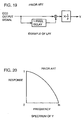
- the LPF with this end is implemented for example by a circuit shown in Fig. 19.
- An LPF 20 includes a one-pixel delay circuit 22 receiving an output signal from the CCD, an adder circuit 24 for adding the output signal received from the CCD and the signal received from one-pixel delay circuit 22 for output, and an attenuator 26 for reducing the intensity of a signal by half.
- the intensity of a Y signal is therefore gradually reduced from the low frequency region and reaches 0 at Nyquist frequency fn as shown in Fig. 20.
- the horizontal resolution for a luminance signal within a single field will be H and the vertical resolution will be V/2. More specifically, the resolution in the vertical direction is half the number of pixels arranged in the CCD.
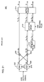
- Fig. 21 is a block diagram schematically showing the structure of a conventional color separation circuit 500 which separates three primary color signals R, G, and B from a CCD output signal.
- Color separation circuit 500 includes a sample-hold circuit 502 performing a sampling and holding (S&H) to a received CCD output signal in response to a sampling pulse SP1 and outputting a signal S1 (Ye+Mg, ... in the n-th line), a sample-hold circuit 504 for performing a sampling and holding to a received CCD output signal in response a sampling pulse SP2 in a phase 180 different from that of sampling pulse SP1 and outputting a signal S2 (Cy+G, ... in the n-th line), an adder circuit 506 for adding received signals S1 and S2 and outputting an added signal S1+S2, and a subtracter circuit 508 for outputting a differential signal S1-S2 between received signals S1 and S2.
- S&H sampling and holding
- a 1H delay line 510 for delaying received signal S1-S2 by one horizontal scanning interval for output
- Fig. 22 is a diagram schematically showing the relation between signals output from CCD 10 and sample-hold pulses SP1 and SP2 for sampling and holding the signals.
- signal S1 sampled and held in response to sampling pulse SP1 is a sum signal of signal Ye and signal Mg for the n-th line.
- Signal S2 sampled and held in response to sampling pulse SP2 is a sum signal of signal Cy and signal G.
- Signal S1 produced by sampling and holding the output signal from the n+1-th line in the CCD in the even-numbered field in response to sampling pulse SP1 is a sum signal of signal Ye and signal G
- signal sampled and held in response to sampling pulse SP2 is a sum signal of signal Cy and signal Mg.
- luminance signal CL luminance signal
- color differential signals CR and CB are necessary for the scanning line.
- color signals are produced/separated in the n+1-th line by using color differential signal CB obtained from the n+1-th line and color differential signal CR obtained from the n-th line.
- signal S1-S2 (CR, CB, ...) output from subtracter circuit 508 and a signal (CB, CR, ...) obtained by passing the signal through 1H delay line 510 are input to selecting circuit 512 switched in response to a line selecting pulse, so that color differential signal S1-S2 one scanning line before may be used as a color differential signal for the scanning line which is currently being read.
- selecting circuit 512 directly outputs signal S1-S2 corresponding to the presently read scanning line to matrix circuit 514 as color differential signal CR if the signal is signal CR, and at the same time outputs a color differential signal one scanning line before which is output from 1H delay line 510 as signal CB to matrix circuit 514.
- signal from 1H delay line 510 is output as color differential signal CR and signal S1-S2 from subtracter circuit 508 is output as color differential signal CB to matrix circuit 514 if color differential signal S1-S2 read out from the present scanning line corresponds to signal CB.
- Signals S1 and S2 result from sampling and holding the output signal of the CCD in response to sampling frequency fn.
- Fig. 23 shows the frequency characteristic of signals S1 and S2.
- Signals S1 and S2 result from sampling and holding, the response of which gradually decreases from the low frequency region and reaches 0 at frequency fn/2.
- Luminance signal CL, color differential signals CR and CB and RGB signal resulting from these signals have similar frequency characteristic as Fig. 23.
- the horizontal resolution of the RGB signal is therefore H/2.
- the vertical resolution within a single field is V/4 for signals CR and CB, and V/2 for luminance signal CL.
- the vertical resolution is about V/4.
- the resolution corresponding to only 1/2 to 1/4 the number of effective pixels can be obtained for RGB.
- Another object of the invention is to provide a method of color separation permitting a luminance signal and color differential signals corresponding to each pixel to be produced based on output signals independently read out from all the pixels of a CCD.
- Yet another object of the invention is to provide a single CCD type color camera capable of restricting a ghost color signal at edges of an image and improving picture quality.
- the present invention is directed to a single CCD color camera including a solid state imaging device and a color separation circuit.
- the solid state imaging device has photoelectric conversion elements corresponding to pixels and arranged in an array.
- the solid state imaging device includes a color filter array in which color differentially ordered color filters corresponding to the photoelectric conversion elements are arranged on the side of its light receiving surface, and green and three kinds of complementary color filters are provided corresponding to four pixels in an arbitrary set of two rows and two columns.
- the color separation circuit produces a color signal corresponding to the central position of the set of four pixels on the basis of output signals from pixels in two rows and two columns among four rows and two columns including the four pixels in response to output signals independently read out from all the pixels by the solid state imaging device.
- the color separation circuit includes a storing circuit for storing signals sequentially output from the solid state imaging device, and an operation circuit for producing a luminance signal and color differential signals corresponding to the differences in intensity between a green signal and the other two primary color signals for each set of four pixels and producing a color signal from the luminance signal and the color differential signals.
- the operation circuit produces a color signal corresponding to the central position by a linear operation to output signals from a set of pixels in two rows and two columns including a pixel in the y-th row and the x-th column (x, y) stored in the storing circuit.
- the operation circuit i produces a color differential signal by output signals from a set of pixels in two rows and two columns if photoelectric conversion elements to output a signal including a prescribed primary color signal among photoelectric conversion elements corresponding to complementary color filters in the pixels in the two rows and two columns are diagonally arranged,
- ii) produces a color differential signal by output signals from a set of adjacent pixels in two rows and two columns to share two pixels among the pixels in two rows and two columns if photoelectric conversion elements to output a signal including a prescribed primary color signal among photoelectric conversion elements corresponding to complementary color filters in the pixels in two rows and two columns are not diagonally arranged.
- a method of separating a color signal in a single CCD type color camera including a solid state imaging device having a color differentially ordered color filter array and a corresponding photoelectric conversion element array includes the steps of:
- a method of separating a color signal in a single CCD color camera including a color filter array having color differentially ordered filters in which green and three kinds of complementary colors correspond to four pixels in an arbitrary set of two rows and two columns and a solid state imaging device having photoelectric conversion elements corresponding to the pixels arranged in an array including the steps of:
- a main advantage of the present invention resides in that if the number of effective pixels in the CCD is H in the horizontal direction and V in the vertical direction, an RGB signal can be produced for each of (H-1) ⁇ (V-1) pixels, and therefore a high resolution may be implemented.
- Another advantage of the present invention resides in that images free from picture quality deterioration may be reproduced while restricting generation of ghost color signals if the brightness of an object changes and edges whose luminance levels abruptly change exist.
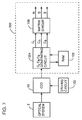
- Fig. 1 is a block diagram schematically showing the structure of a main portion of a color separation circuit 100 according to the invention in comparison with the structure of the conventional color separation circuit 200 shown in Fig. 21.
- Color separation circuit 100 includes an optical system receiving light from an object, a CCD 10 converting an optical image formed by optical system 2 into an electrical signal, a driving circuit 102 for driving an independent reading from all the pixels, a CLCRCB generation circuit 104 for generating a luminance signal CL and color differential signals CR and CB based on an output signal received from CCD 10, a random access memory 106 (hereinafter RAM) capable of transmitting/receiving a reading signal D(x, y), luminance signal CL, and color differential signals CR and CB from CCD 10 to/from CLCRCB generation circuit 104 and storing these signals for at least two scanning lines, and a matrix circuit 108 for separating and outputting three primary color signals R, G and B from a signal received from CLCRCB generation circuit 104 through a prescribed operation.
- a CCD 10 converting an optical image formed by optical system 2 into an electrical signal
- a driving circuit 102 for driving an independent reading from all the pixels
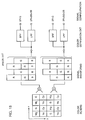
- Fig. 2 is a diagram schematically showing the arrangement of a color filter array according to the embodiment and a reading of a signal from CCD 10 including the arrangement of color filter array.
- driving circuit 102 generates a driving pulse without mixing two pixels in the vertical direction in CCD 10 unlike the conventional example in Fig. 21.
- An output signal from CCD 10 is read out on a frame-basis rather than on the field-basis as shown in Figs. 17A and 17B.
- each pixel (x, y) and the filter color in a CCD output signal as described above may be represented as follows if n is a natural number.
- Mg and G color filters belong to odd numbered rows and Ye and Cy color filters belong to even numbered robs for ease of illustration, the present invention is not limited to such an arrangement, and is similarly applicable for example to a color filter arrangement one row shifted from this arrangement.
- CLCRCB generation circuit 104 when independent reading of all the pixels as described in conjunction with Fig. 2 is performed will be detailed.
- Fig. 3 is a diagram schematically showing data processing in CLCRCB generation circuit 104 and data exchange with RAM 106.
- the prefix c represents one of L, R and B
- CL(x, y) represents a luminance signal
- CR(x, y) a first color differential signal
- CB(x, y) a second color differential signal.
- signal Cc(x, y) is a signal corresponding to the central position of the four pixels, this is only for ease of representation, and the signal may be defined as a signal corresponding to the pixel (x, y) in a one-to-one correspondence with pixel (x, y).
- Cc(x, y) Kc(x, y) ⁇ D(x, y)+Kc(x+1, y) ⁇ D(x+1, y)+Kc(x, y+1) ⁇ D(x, y+1)+Kc(x+1, y+1) ⁇ D(x+1, y+1)
- a luminance signal and a color differential signal corresponding to the pixel (1, 2) circled in Fig. 2 will be generated according to the process as described above.
- the set of pixels in two rows and two columns including the pixel (1, 2) includes pixel (1, 2), pixel (2, 2), pixel (1, 3) and pixel (2, 3).
- a color filter corresponding to pixel (1, 2) is Cy
- a color filter corresponding to pixel (2, 2) is Ye
- a color filter corresponding to pixel (1, 3) is Mg
- a color filter corresponding to pixel (2, 3) is G.
- Expression (16) is formed by modifying expression (15) taking advantage of the relation between the color of the filter and factor KL(X, Y) as described above, and expression (17) is formed by modifying expression (16) using expressions (1) to (3).
- luminance signal CL(1, 2) corresponding to pixel (1, 2) may be obtained.
- First color differential signal CR(1, 2) may be also produced as follows based on expression (14).
- Expression (19) is formed by modifying expression (18) taking advantage of the relation between the color of the filter of pixel (X, Y) and factor KR(X, Y), and expression (20) is formed by modifying expression (19) using expressions (1) to (3).
- first color differential signal CL(1, 2) corresponding to pixel (1, 2) may be produced.
- Second color differential signal CB(1, 2) may be also produced as follows similarly to the case of first color differential signal CB(1, 2).
- CB(1, 2) KB(1, 2) ⁇ (1, 2)+KB(2, 2) ⁇ D(2, 2)+KB(1, 3) ⁇ D(1, 3)+KB(2, 3) ⁇ D(2, 3)
- Expression (22) is formed by modifying expression (21) also taking advantage of the relation between the color of the filter of pixel (X, Y) and factor KB(X, Y), and expression (23) is formed by modifying expression (22) using expressions (1) to (3).
- luminance signal CL and color differential signals CR and CB may be generated corresponding to each of the pixels constituting CCD 10.
- CLCRCB generation circuit 104 may generate luminance signal CL and color differential signals CR and CB through the above-described operation based on the relation.
- Matrix circuit 108 separates a RGB signal corresponding to each of the pixels of the CCD through the following operations to output signal CL, signal CR and signal CB received from CLCRCB generation circuit 104.
- G(x, y) ⁇ 2CL(x, y)-2CR(x, y)-2CB(x, y) ⁇ /10
- R(x, y) ⁇ CL(x, y)+4CR(x, y)-CB(x, y) ⁇ /10
- B(x, y) ⁇ CL(x, y)-CR(x, y)+4CB(x, y) ⁇ /10
- an RGB signal may be generated for each of all the pixels in CCD 10.
- a resulting horizontal resolution is H-1
- a resulting vertical resolution is V-1.
- the meaning of "-1" used in the horizontal and vertical resolutions is that an RGB signal is produced corresponding to a single pixel (x, y) included in the set of pixels arranged in two rows and two columns according to this embodiment, and therefore the number of effective columns/rows in the pixel array is reduced by one both in the horizontal and vertical directions because the set of pixels in two rows and two columns can not be picked up any longer with respect to the last column or row.
- color separation circuit 100 exchanges signal D(x, y), luminance signal CL, and color differential signals CR and CB from CCD 10 with CLCRCB generation circuit 104, and includes RAM 106 capable of storing these signals for at least two scanning lines.
- luminance signal CL, first and second color differential signals CR and CB can be generated by processing by the CLCRCB generation circuit based on the read out signals within the frame memory.
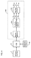
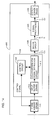
- Fig. 4 is a block diagram schematically showing the structure of a main portion of a color separation circuit 200 according to a second embodiment of the invention having such a structure.
- color separation circuit 200 includes a frame memory 110 for storing the entire one frame of signals D(x, y) read out from CCD 10, and CLCRCB generation circuit 204 generates luminance signal CL, first and second color differential signals CR and CB based on data received from the frame memory, as opposed to the structure of color separation circuit 100 according to the first embodiment. Since the other features are similar to the structure of color separation circuit 100 according to the first embodiment, and therefore the same portions are attached with the same reference numerals and characters and the description will not be repeated.
- luminance signal CL and first and second color differential signals CL and CB are generated according to the process represented by expression (14) in the first embodiment.
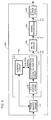
- Fig. 5 is a block diagram showing more in detail the structure of CLCRCB generation circuit 204 in the structure shown in Fig. 4.
- color separation circuit 200 includes a signal processing circuit 200 for producing video signals (i.e. luminance signal Y and color differential signals Cu and Cv produced through well known gamma correction and white balance correction) in response to a signal received from matrix circuit 108, and an output buffer 230 externally outputting the video signal received from signal processing circuit 220.
- video signals i.e. luminance signal Y and color differential signals Cu and Cv produced through well known gamma correction and white balance correction
- Color separation circuit 200 may be implemented as an ASIC (application-specific integrated circuit).
- frame memory 110 can form a dynamic random access memory (hereinafter DRAM) having a storage capacity for H ⁇ V pieces of pixel data where the number of horizontal pixels is H and the number of vertical pixels is V in CCD 10.
- DRAM dynamic random access memory
- CLCRCB generation circuit 204 includes an input buffer 206 receiving from frame memory 110, one block of data corresponding to a plurality of pixels necessary for a prescribed image processing, a control circuit 208 controlling addressing of a data block to be read out from frame memory 110, and a color differential signal separation circuit 210 controlled by control circuit 208 for performing a separation processing to one block of data in the input buffer to obtain for each pixel luminance signal CL, and first and second color differential signals CL and CB.
- input buffer 206 stores data corresponding to 9 ⁇ 9 pixels as one block.
- Input buffer 26 can be formed of a static random access memory (hereinafter SRAM) having a capacity of storing data for the above 9 ⁇ 9 pixels.
- SRAM static random access memory
- Color differential signal separation circuit 210 is controlled by control circuit 208 to sequentially read out data for 2 ⁇ 2 pixels among data for 9 ⁇ 9 pixels stored in input buffer 206, and generates luminance signal CL, and first and second color differential signals CL and CB depending upon the color of a color filter corresponding to each pixel and according to expression (14).
- Matrix circuit 108 receives an output from color differential signal separation circuit 210, outputs three primary color signals R, G and B corresponding to the central position of each of 2 ⁇ 2 pixels, and signal processing circuit 220, though not limited, generates a video signals (i.e. luminance signal Y and color differential signals Cv and Cu produced through well known gamma correction and white balance correction) based on the primary color signals.
- a video signals i.e. luminance signal Y and color differential signals Cv and Cu produced through well known gamma correction and white balance correction
- Output buffer 230 accumulates one block of video signals (data for 8 ⁇ 8 pixels in the JPEG coding) output from signal processing circuit 220, and externally outputs the data on a block-basis.
- Output buffer 230 can be formed of an SRAM having a capacity of storing data for 8 ⁇ 8 pixels as described above, though not limited thereto.
- a JPEG coding circuit (not shown) performs a JPEG coding, and the coded data is for example stored in a flash memory.
- the above-described processing is repeatedly performed to one frame of data stored in frame memory 110, and compressed data corresponding to images for one frame is consequently stored in the flash memory.
- Fig. 6 is a flow chart for use in illustration of the operation of color separation circuit 200 shown in Fig. 5.
- input buffer 206 is controlled by control circuit 208 to take in a unit data block for processing (data for 9 ⁇ 9 pixels) (step S100).
- Color differential signal separation circuit 210 then receives data for 2 ⁇ 2 pixels to perform a separation processing of color differential signals from the unit data in input buffer 206 in response to an address designated by control circuit 208 (step S102).
- Matrix circuit 108 receives an output from color differential signal separation circuit 210 and outputs three primary color signals R, G and B corresponding to the central position of each of 2 ⁇ 2 pixels (step S114).
- Signal processing circuit 220 then generates an NTSC signal, video signals Y, Cu, Cv based on the three primary color signals (step S116).
- Output buffer 230 accumulates video signals output from signal processing circuit 220 (step S118).
- step S120 it is determined whether or not color differential signal separation processing to one block of data (data for 9 ⁇ 9 pixels) stored in input buffer 206 has been completed.
- step S120 If the processing has been completed (step S120), Y, Cu and Cv data corresponding to 8 ⁇ 8 pixels is output from output buffer 230, and the JPEG coding circuit performs a JPEG coding (image data compression processing) to the received data (step S122).
- the coded data is also stored in the flash memory (step S124).
- the above-described processing is repeatedly performed to one frame of data stored in frame memory 110, and the one frame of image data is compressed and stored.
- RGB signals may be generated corresponding to each of all the pixels in CCD 10 as is the case with color separation circuit 100 in the first embodiment. Therefore, an improved resolution, H-1 in the horizontal direction and V-1 in the vertical direction is implemented as compared to the conventional color separation circuit.
- the arrangement of color filter array is not limited to the color differentially ordered arrangement as shown in Fig. 2, but the invention is applicable to other color filter array arrangements by changing factors KL, KR and KB accordingly.
- a color separation circuit 300 according to a third embodiment of invention has basically the same structure as that of color separation circuit 100 according to the first embodiment. However, as will be described below, the third embodiment is directed to restriction of generation of a ghost color signal by replacing CLCRCB generation circuit 104 with CLCRCB generation circuit 304.
- color separation circuit 300 according to the third embodiment shown in Fig. 7 is essentially identical to color separation circuit 100 according to the first embodiment shown in Fig. 1 with a difference being that CLCRCB generation circuit 104 is replaced with CLCRCB generation circuit 304.
- Fig. 8 is a diagram schematically showing the arrangement of color filter array according to the embodiment and how a signal is read out from CCD 10 having such a color filter array.
- CCD 10 performs an independent reading operation to all the pixels. More specifically, driving circuit 102 generates a driving pulse without mixing two pixels in the vertical direction.
- An output signal from CCD 10 is a so-called frame reading signal rather than a field reading signal shown in Fig. 17.
- Mg and G are alternately arranged in the horizontal direction (x-direction) in the 0-th line in the vertical direction (y-direction), Mg and G are alternately output as a signal read out from CCD 10 for a scanning line corresponding the line.
- signals Ye and Cy are alternately output.
- each pixel (x, y) in a CCD output signal and a filter color as described above may be represented as follows if n is a natural number.
- Mg and G color filters belong to even numbered rows and Ye and Cy color filters belong to odd numbered rows for ease of illustration, the present invention is not limited to such an arrangement, and is similarly applicable for example to a color filter arrangement one row shifted from this arrangement.
- output signals are independently read out from all the pixels in CCD 10, and these signals are stored in RAM 106.
- luminance signal CL(x, y), first color differential signal CR(x, y) and second color differential signal CB(x, y) may be generated for each pixel (x, y) through the following operations.
- an output signal from a photoelectric conversion element corresponding to pixel (x, y) in CCD 10 is represented as D(x, y).
- a luminance signal and two color differential signals can be extracted through the linear operation represented by expression (14) to output signals from pixels (x, y), (x+1, y), (x, y+1) and (x+1, y+1) in two rows and two columns including pixel (x, y).
- a luminance signal and color differential signals corresponding to pixel (0, 0) shown in Fig. 8 will be produced by way of illustration.
- second color differential signal CB (0, 0) is produced by the following expression (29):
- the luminance signal and two color differential signals for pixel (0, 0) can be produced using output signals from pixels (0, 0), (1, 0), (0, 1), and (1, 1).
- a luminance signal and color differential signals may be produced through a linear operation of output signals from pixels (x, y), (x+1, y), (x, y+1), and (x+1, y+1) in two rows and two columns including that pixel (x, y).
- a luminance signal and two color differential signals can be produced for each pixel, and therefore a color separation circuit with a higher resolution than a conventional color separation circuit can be advantageously implemented.
- the intensity of light incident to the arrangement of CCD pixels has a change H1 in luminance level in the horizontal direction (an edge where the luminance level changes between the left and right end of the picture plane) will be considered.
- H1 in luminance level in the horizontal direction an edge where the luminance level changes between the left and right end of the picture plane
- the luminance level changes by b/a (b>a) toward the horizontal direction (x-axis).
- a luminance signal and color differential signals for pixel (0, 0) will be produced as follows by way of illustration.
- color differential signals may be produced for pixel (0, 2) as follows.
- a ghost color is generated if there exists a great luminance change (edge) in the horizontal direction. If the image is reproduced on the picture plane, the ghost color appears at the portion essentially without any color, which results in picture quality deterioration. Also in the process of producing R, G and B signals for three primary colors from signals CL, CR and CB, a ghost luminance signal is generated because of a ghost color signal component, resulting in deterioration of the luminance signal.
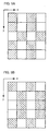
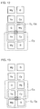
- Fig. 9A is a diagram showing the arrangement of filters to output a color signal including an R signal component for the color filter array in Fig. 2, with the arrangement of pixels to output the signal having the R signal component being shaded.
- Fig. 9B is a diagram showing the arrangement of pixels to output a signal including a B signal component being shaded.
- the R signal is included in output signals from pixels corresponding to a magenta color filter and a yellow color filter among the arrangement of color filters in Fig. 8.
- the B signal component is included in output signals from pixels corresponding to a magenta color filter and a cyan color filter.
- an output signal having an R signal component is obtained only from the side of lower luminance level, and there is no R signal component on the side of higher luminance level.
- a large ghost color signal component is generated in color differential signal CR(0, 0) accordingly.
- a pixel to output a signal having a B signal component exists on both sides of higher and lower luminance levels.
- a ghost color signal for color differential signal CB (0, 0) has an absolute value smaller than a ghost color signal component appearing for color differential signal CR (0, 0).
- the color differential signal CR needs to be produced based on signals from a set of pixels in two rows and two columns in which pixels to output a R signal component are diagonally arranged in order to suppress generation of a ghost color signal. This also applies to color differential signal CB.
- CLCRCB generation circuit 304 will be described when an independent reading is performed to all the pixels in CCD 10 as shown in Fig. 7.
- the method is expressed as producing a luminance signal and color differential signals for a pixel in the center of four pixels in two rows and two columns based on output signals from the pixels.
- the method may be expressed as generating color differential signals for pixel (x, y) from output signals in two rows and two columns of pixels (x, y), (x+1, y), (x, y+1), and (x+1, y+1) including the pixel.
- the luminance signal and color differential signals for pixel (x, y) among these four pixels are assumed to be a luminance signal and color differential signals for the central position, the expression is substantially the same as following description.
- an output signal D(x, y) is for example a magenta color filter
- the signal is specifically expressed as Mg(x, y).
- Figs. 10 to 13 are diagrams for use in illustration of the operation of CLCRCB generation circuit 304 in color separation circuit 300 according to the invention.
- Fig. 10 shows a set of pixels in two rows and two columns used in calculating color differential signals in the central position surrounded by pixels (0, 0), (1, 0), (1, 0) and (1, 1).
- Fig. 11 shows a set of pixels in two rows and two columns used in calculating color differential signals in the central position surrounded by pixels (0, 1), (1, 1), (0, 2) and (1, 2) shown in Fig. 8.
- Fig. 12 shows a set of pixels in two rows and two columns used in calculating color differential signals in the central position surrounded by pixels (0, 2), (1, 2), (0, 3) and (1, 3) shown in Fig. 8.
- Fig. 13 shows a set of pixels in two rows and two columns used in calculating color differential signals in the central position surrounded by pixels (0, 3), (1, 3), (0, 4) and (1, 4) as shown in Fig. 8.
- luminance signal CL and color differential signal CB in the central position surrounded by pixels (0, 0), (1, 0), (0, 1) and (1, 1) are both calculated based on output signals from these four pixels.
- color differential signal CR is calculated based on output signals from a set of pixels in two rows and two columns shifted by one pixel in the y-direction.
- the luminance signal and color differential signal CR in the central position surrounded by pixels (0, 1), (1, 1), (0, 2) and (1, 2) are calculated based on output signals from these four pixels.
- color differential signal CB is calculated from a set of pixels in two rows and two columns shifted by one pixel in the - y-direction.
- luminance signal CL and color differential signal CR corresponding to the central position surrounded by pixels (0, 2), (1, 2), (0, 3) and (1, 3) are calculated from the four pixels in two rows and two columns.
- color differential signal CB is calculated based on output signals from pixels in two rows and two columns shifted by one pixel in the y-direction.
- luminance signal CL and color differential signal CB in the central position surrounded by pixels (0, 3), (1, 3), (0, 4) and (1, 4) are operated based on output signals from these four pixels.
- color differential signal CR is calculated based on output signals from pixels in two rows and two columns shifted by one pixel in the - y direction.
- CLCRCB generation circuit 104 By the operation of CLCRCB generation circuit 104 as described above, the effect of suppressing generation of ghost color signals by luminance signal CL and color differential signals CR and CB may be confirmed as follows.
- color differential signals for pixel (0, 0) will be derived.
- color differential signal CB(0, 0) will be calculated as follows.
- CB(0, 0) S(b-a)
- Color differential signals corresponding to a single pixel are calculated for each two rows in the vertical direction, its vertical resolution is V/2 if there is V pixels in the vertical direction.
- V/2 if there is V pixels in the vertical direction.
- luminance signal CL and color differential signals CR and CB can be generated for each of all the pixels constituting CCD 10.
- CLCRCB generation circuit 104 can generate luminance signal CL and color differential signals CR and CB through the above-described operation based on the relation.
- matrix circuit 108 shown in Fig. 7 is the same as the first embodiment.
- Matrix circuit 108 therefore performs operations represented by expressions (24) to (26) to signals CL, CR and CB received from CLCRCB generation circuit 304 to separate a RGB signal corresponding to each of all of the pixels in the CCD.
- An RGB signal corresponding to each of all the pixels in CCD 10 can be generated.
- an improved resolution, H-1 in the horizontal direction and V-1 in the vertical direction can be implemented as opposed to a conventional color separation circuit.
- ghost colors may be advantageously suppressed as described above.
- a color separation circuit 400 according to a fourth embodiment of the invention has essentially the same structure as color separation circuit 200 according to the second embodiment. However, the fourth embodiment is directed to suppressing generation of a ghost color signal by replacing color signal separation circuit 210 with a color differential signal separation circuit 410 as will be described later.
- color separation circuit 300 according to the fourth embodiment shown in Fig. 14 is essentially identical to the structure of color separation circuit 200 shown in Fig. 2 with a difference being that color differential signal separation circuit 210 is replaced with a color differential signal separation circuit 410.
- color separation circuit 400 includes a frame memory 110 for storing the entire one frame of signal D(x, y) from CCD 10, and a CLCRCB generation circuit 404 generates luminance signal CL, and first and second color differential signals CR and CB in response to data from the frame memory, as opposed to color separation circuit 300 according to the third embodiment. Since the other features are the same as those of color separation circuit 300 according to the third embodiment, the same portions are denoted by the same reference numerals and characters and a description will not be repeated here.
- luminance signal CL and first and second color differential signals CR and CB are generated according to the method described in conjunction with Figs. 10 to 13 according to the third embodiment.
- Fig. 15 is a flow chart for use in illustration of the operation of color separation circuit 400 shown in Fig. 14.
- input buffer 206 is controlled by control circuit 208 to take in a unit data block for processing (data for 9 ⁇ 11 pixels) from frame memory 110 (step S200).
- Color differential signal separation circuit 410 then receives data for 4 ⁇ 2 pixels for a separation processing of color differential signals from the unit data in input buffer 206 in response to addresses designated by control circuit 208 (step S202).
- Color differential signal separation circuit 410 performs the processing described in conjunction with Figs. 10 to 13 depending upon the color of a color filter corresponding to each pixel which is defined based on the addresses of 4 ⁇ 2 pixels. More specifically, in the arrangement of color filters shown in Fig. 8, a processing corresponding to the values of x and y of a pixel (x, y) corresponding to the position to produce color differential signals among the 4 ⁇ 2 pixels is performed (steps S206 to S212).
- Matrix circuit 108 receives an output from color differential signal separation circuit 210 and outputs three primary color signals R, G and B corresponding to the central position in each of 2 ⁇ 2 pixels (step S214).
- Signal processing circuit 220 then generates Y, Cu and Cv signals, video signals based on the three primary color signals (step S216).
- Output buffer 230 accumulates video signals output from signal processing circuit 220 (step S218).
- step S220 it is determined whether or not a color differential signal separation processing has been completed to one block of data (data for 9 ⁇ 11 pixels) stored in input buffer 206 (step S220).
- step S220 If it is determined that the processing to the one block of data has been completed (step S220), Y, Cu and Cv data corresponding to 8 ⁇ 8 pixels is output from output buffer 230, and the JPEG coding circuit performs a JPEG coding processing (image data compressing processing) to the data (step S222).
- the coded data is accumulated in the flash memory (step S224).
- the above-described processing is repeatedly performed to one frame of data stored in frame memory 110, and one frame of image data is compressed and stored.
- an RGB signal corresponding to each of all the pixels in CCD 10 can be generated. Therefore, as is the third embodiment, an improved resolution, H-1 in the horizontal direction and V-1 in the vertical direction may be implemented as opposed to a conventional color separation circuit.
- ghost colors may be advantageously suppressed as is the third embodiment.
Landscapes
- Engineering & Computer Science (AREA)
- Multimedia (AREA)
- Signal Processing (AREA)
- Physics & Mathematics (AREA)
- Spectroscopy & Molecular Physics (AREA)
- Color Television Image Signal Generators (AREA)
Applications Claiming Priority (6)
| Application Number | Priority Date | Filing Date | Title |
|---|---|---|---|
| JP7728396 | 1996-03-29 | ||
| JP77283/96 | 1996-03-29 | ||
| JP8077283A JPH09271029A (ja) | 1996-03-29 | 1996-03-29 | 単板式カラーカメラおよび色信号の分離方法 |
| JP20194896 | 1996-07-31 | ||
| JP201948/96 | 1996-07-31 | ||
| JP20194896 | 1996-07-31 |
Publications (3)
| Publication Number | Publication Date |
|---|---|
| EP0800317A2 true EP0800317A2 (de) | 1997-10-08 |
| EP0800317A3 EP0800317A3 (de) | 1997-12-03 |
| EP0800317B1 EP0800317B1 (de) | 2002-06-05 |
Family
ID=26418389
Family Applications (1)
| Application Number | Title | Priority Date | Filing Date |
|---|---|---|---|
| EP97105161A Expired - Lifetime EP0800317B1 (de) | 1996-03-29 | 1997-03-26 | Farbkamera mit einem einzigen CCD-Farbbildsensor mit höherer Auflösung, der fähig ist, Geisterfarberzeugung zu begrenzen |
Country Status (4)
| Country | Link |
|---|---|
| US (1) | US6323901B1 (de) |
| EP (1) | EP0800317B1 (de) |
| KR (1) | KR100447916B1 (de) |
| DE (1) | DE69712969T2 (de) |
Cited By (6)
| Publication number | Priority date | Publication date | Assignee | Title |
|---|---|---|---|---|
| EP1083754A2 (de) | 1999-09-10 | 2001-03-14 | Sony Corporation | Bildaufnahmegerät |
| EP1038159A4 (de) * | 1997-12-08 | 2002-08-07 | Intel Corp | Neuer auf flankendetektion gestützter geraüschunterdrückungsalgorithmus |
| EP0969674A3 (de) * | 1998-07-03 | 2004-01-02 | Canon Kabushiki Kaisha | Bildaufnahmegerät zur Verarbeitung von Bildsignalen in Blöcken |
| WO2007087119A3 (en) * | 2006-01-12 | 2007-11-22 | Micron Technology Inc | Method and apparatus for producing bayer color mosaic interpolation for imagers |
| EP1367837A4 (de) * | 2001-01-25 | 2009-04-01 | Nikon Corp | Bildverarbeitungsverfahren, bildverarbeitungsprogramm und bildprozessor |
| DE202007019236U1 (de) | 2007-11-02 | 2011-11-09 | Valentina Anzupowa | Farbteiler-Bildwandler-Gruppe mit teildurchlässigen Spiegeln und Mosaikfarbfiltern |
Families Citing this family (6)
| Publication number | Priority date | Publication date | Assignee | Title |
|---|---|---|---|---|
| JP3925588B2 (ja) * | 1997-11-25 | 2007-06-06 | セイコーエプソン株式会社 | 画像処理装置、画像処理方法および画像処理制御プログラムを記録した媒体 |
| JP4006075B2 (ja) * | 1998-01-30 | 2007-11-14 | キヤノン株式会社 | Cmosセンサ及び撮像システム |
| US6900838B1 (en) * | 1999-10-14 | 2005-05-31 | Hitachi Denshi Kabushiki Kaisha | Method of processing image signal from solid-state imaging device, image signal processing apparatus, image signal generating apparatus and computer program product for image signal processing method |
| KR100423616B1 (ko) * | 2002-04-12 | 2004-03-22 | 주식회사 레이시스 | 영상 보정기능이 있는 ccd 카메라 |
| JP2005197922A (ja) * | 2004-01-06 | 2005-07-21 | Fuji Xerox Co Ltd | 画像読取装置 |
| DE102010030108B4 (de) | 2010-06-15 | 2014-12-04 | Fraunhofer-Gesellschaft zur Förderung der angewandten Forschung e.V. | Farbbildsensor |
Family Cites Families (24)
| Publication number | Priority date | Publication date | Assignee | Title |
|---|---|---|---|---|
| GB2014397B (en) * | 1978-02-10 | 1982-08-18 | Hitachi Ltd | Solid-state colour imaging device |
| DE3381818D1 (de) | 1982-12-14 | 1990-09-20 | Matsushita Electric Industrial Co Ltd | Festkoerper-farbabbildungsanordnung. |
| JPH0628450B2 (ja) * | 1983-01-28 | 1994-04-13 | 松下電器産業株式会社 | 固体撮像装置 |
| EP0119862B1 (de) * | 1983-03-17 | 1990-12-27 | Nec Corporation | Festkörperfarbabbildungsgerät |
| JPS6055781A (ja) * | 1983-09-07 | 1985-04-01 | Nec Corp | 固体撮像素子 |
| JPS60214183A (ja) * | 1984-04-09 | 1985-10-26 | Nec Corp | カラ−撮像装置 |
| US4697208A (en) * | 1985-06-13 | 1987-09-29 | Olympus Optical Co., Ltd. | Color image pickup device with complementary color type mosaic filter and gamma compensation means |
| JPS631276A (ja) * | 1986-06-20 | 1988-01-06 | Olympus Optical Co Ltd | カラ−撮像装置 |
| US4998162A (en) * | 1988-08-22 | 1991-03-05 | Sony Corporation | Video camera |
| US4945406A (en) * | 1988-11-07 | 1990-07-31 | Eastman Kodak Company | Apparatus and accompanying methods for achieving automatic color balancing in a film to video transfer system |
| US5457494A (en) * | 1988-11-21 | 1995-10-10 | Canon Kabushiki Kaisha | Image pickup signal processing apparatus |
| JP2668444B2 (ja) * | 1989-11-28 | 1997-10-27 | キヤノン株式会社 | 撮像装置 |
| JP2733859B2 (ja) * | 1989-09-28 | 1998-03-30 | キヤノン株式会社 | カラー撮像装置 |
| JP3035930B2 (ja) * | 1989-10-19 | 2000-04-24 | ソニー株式会社 | カラー固体撮像装置 |
| KR920006601Y1 (ko) | 1989-12-31 | 1992-09-21 | 삼성전자 주식회사 | 보색 필터 ccd를 이용한 원색 신호 출력회로 |
| JP2942903B2 (ja) * | 1990-11-05 | 1999-08-30 | キヤノン株式会社 | ディジタル・カメラ信号処理装置 |
| EP0570204B1 (de) * | 1992-05-13 | 1996-07-10 | Matsushita Electric Industrial Co., Ltd. | Festkörperbildaufnahmevorrichtung mit einer Farbfiltermatrix |
| JPH06133319A (ja) * | 1992-10-16 | 1994-05-13 | Canon Inc | カラー撮像装置 |
| JP3615778B2 (ja) * | 1993-04-05 | 2005-02-02 | 日本フィリップス株式会社 | カラー撮像装置 |
| JP3647052B2 (ja) * | 1993-04-15 | 2005-05-11 | キヤノン株式会社 | 撮像装置 |
| JP2931520B2 (ja) * | 1993-08-31 | 1999-08-09 | 三洋電機株式会社 | 単板式カラービデオカメラの色分離回路 |
| US6031569A (en) * | 1994-02-28 | 2000-02-29 | Canon Kabushiki Kaisha | Image sensing method and apparatus utilizing the same |
| JPH07288824A (ja) * | 1994-04-14 | 1995-10-31 | Asahi Optical Co Ltd | 輝度信号生成装置 |
| JP3392564B2 (ja) * | 1995-02-27 | 2003-03-31 | 三洋電機株式会社 | 単板式カラービデオカメラ |
-
1997
- 1997-03-26 DE DE69712969T patent/DE69712969T2/de not_active Expired - Fee Related
- 1997-03-26 US US08/824,296 patent/US6323901B1/en not_active Expired - Fee Related
- 1997-03-26 EP EP97105161A patent/EP0800317B1/de not_active Expired - Lifetime
- 1997-03-28 KR KR1019970011194A patent/KR100447916B1/ko not_active Expired - Fee Related
Cited By (11)
| Publication number | Priority date | Publication date | Assignee | Title |
|---|---|---|---|---|
| EP1038159A4 (de) * | 1997-12-08 | 2002-08-07 | Intel Corp | Neuer auf flankendetektion gestützter geraüschunterdrückungsalgorithmus |
| EP0969674A3 (de) * | 1998-07-03 | 2004-01-02 | Canon Kabushiki Kaisha | Bildaufnahmegerät zur Verarbeitung von Bildsignalen in Blöcken |
| US6684000B1 (en) | 1998-07-03 | 2004-01-27 | Canon Kabushiki Kaisha | Image sensing device capable of outputting image signals by blocks and processing circuit which processes image signals by blocks |
| EP1083754A2 (de) | 1999-09-10 | 2001-03-14 | Sony Corporation | Bildaufnahmegerät |
| EP1083754A3 (de) * | 1999-09-10 | 2004-11-10 | Sony Corporation | Bildaufnahmegerät |
| US7068314B1 (en) | 1999-09-10 | 2006-06-27 | Sony Corporation | Image pickup apparatus which can eliminate a false color in the spatial frequency band during chromatic signal processing |
| EP1367837A4 (de) * | 2001-01-25 | 2009-04-01 | Nikon Corp | Bildverarbeitungsverfahren, bildverarbeitungsprogramm und bildprozessor |
| US7565007B2 (en) | 2001-01-25 | 2009-07-21 | Nikon Corporation | Image processing method, image processing program, and image processing apparatus |
| WO2007087119A3 (en) * | 2006-01-12 | 2007-11-22 | Micron Technology Inc | Method and apparatus for producing bayer color mosaic interpolation for imagers |
| US7456881B2 (en) | 2006-01-12 | 2008-11-25 | Aptina Imaging Corporation | Method and apparatus for producing Bayer color mosaic interpolation for imagers |
| DE202007019236U1 (de) | 2007-11-02 | 2011-11-09 | Valentina Anzupowa | Farbteiler-Bildwandler-Gruppe mit teildurchlässigen Spiegeln und Mosaikfarbfiltern |
Also Published As
| Publication number | Publication date |
|---|---|
| KR970067935A (ko) | 1997-10-13 |
| DE69712969T2 (de) | 2003-01-09 |
| EP0800317B1 (de) | 2002-06-05 |
| US6323901B1 (en) | 2001-11-27 |
| EP0800317A3 (de) | 1997-12-03 |
| DE69712969D1 (de) | 2002-07-11 |
| KR100447916B1 (ko) | 2004-11-06 |
Similar Documents
| Publication | Publication Date | Title |
|---|---|---|
| US6133953A (en) | Color camera having a single imaging element and capable of restricting unwanted false color signal | |
| US7830431B2 (en) | Simultaneous readout of CMOS APS imagers | |
| EP0800317B1 (de) | Farbkamera mit einem einzigen CCD-Farbbildsensor mit höherer Auflösung, der fähig ist, Geisterfarberzeugung zu begrenzen | |
| US5043817A (en) | Image pick-up apparatus with electronic zooming-in | |
| JP3854662B2 (ja) | 撮像装置 | |
| US6429953B1 (en) | Super resolution scanning using color multiplexing of image capture devices | |
| KR100462260B1 (ko) | 영상픽업장치 | |
| KR100552016B1 (ko) | 디지탈 컬러 카메라 및 색 데이타 분리 방법 | |
| JP3967853B2 (ja) | 固体撮像装置および信号読出し方法 | |
| US5150204A (en) | Solid state image pickup having plural pixels arranged on plural lines | |
| EP1173029A2 (de) | Farbbildaufnahmegerät | |
| JP2000152256A (ja) | 固体撮像素子およびその駆動方法並びにカメラシステム | |
| JP2002084548A (ja) | カラー撮像素子及び撮像装置 | |
| JP2940820B2 (ja) | 単板式カラーカメラおよび色信号の分離方法 | |
| JPH10173868A (ja) | 固体撮像素子およびこれを備えた画像読取装置 | |
| JPWO2002085035A1 (ja) | 固体撮像装置 | |
| JP2000261817A (ja) | 撮像装置 | |
| JP2692486B2 (ja) | 固体撮像装置 | |
| JP3463695B2 (ja) | 撮影装置 | |
| JPH0492590A (ja) | スチルビデオカメラ | |
| JPH0492591A (ja) | スチルビデオカメラ | |
| JPH07147683A (ja) | 固体撮像素子 | |
| JPH0492592A (ja) | 撮像装置 | |
| JPH09271029A (ja) | 単板式カラーカメラおよび色信号の分離方法 | |
| JP2007088733A (ja) | Ccd型単板式カラー固体撮像素子 |
Legal Events
| Date | Code | Title | Description |
|---|---|---|---|
| PUAI | Public reference made under article 153(3) epc to a published international application that has entered the european phase |
Free format text: ORIGINAL CODE: 0009012 |
|
| AK | Designated contracting states |
Kind code of ref document: A2 Designated state(s): DE FR GB |
|
| PUAL | Search report despatched |
Free format text: ORIGINAL CODE: 0009013 |
|
| AK | Designated contracting states |
Kind code of ref document: A3 Designated state(s): DE FR GB |
|
| 17P | Request for examination filed |
Effective date: 19971218 |
|
| 17Q | First examination report despatched |
Effective date: 20000105 |
|
| GRAG | Despatch of communication of intention to grant |
Free format text: ORIGINAL CODE: EPIDOS AGRA |
|
| GRAG | Despatch of communication of intention to grant |
Free format text: ORIGINAL CODE: EPIDOS AGRA |
|
| GRAH | Despatch of communication of intention to grant a patent |
Free format text: ORIGINAL CODE: EPIDOS IGRA |
|
| GRAH | Despatch of communication of intention to grant a patent |
Free format text: ORIGINAL CODE: EPIDOS IGRA |
|
| GRAA | (expected) grant |
Free format text: ORIGINAL CODE: 0009210 |
|
| AK | Designated contracting states |
Kind code of ref document: B1 Designated state(s): DE FR GB |
|
| REG | Reference to a national code |
Ref country code: GB Ref legal event code: FG4D |
|
| REF | Corresponds to: |
Ref document number: 69712969 Country of ref document: DE Date of ref document: 20020711 |
|
| ET | Fr: translation filed | ||
| PLBE | No opposition filed within time limit |
Free format text: ORIGINAL CODE: 0009261 |
|
| STAA | Information on the status of an ep patent application or granted ep patent |
Free format text: STATUS: NO OPPOSITION FILED WITHIN TIME LIMIT |
|
| 26N | No opposition filed |
Effective date: 20030306 |
|
| PGFP | Annual fee paid to national office [announced via postgrant information from national office to epo] |
Ref country code: FR Payment date: 20060308 Year of fee payment: 10 |
|
| PGFP | Annual fee paid to national office [announced via postgrant information from national office to epo] |
Ref country code: DE Payment date: 20060323 Year of fee payment: 10 |
|
| GBPC | Gb: european patent ceased through non-payment of renewal fee |
Effective date: 20070326 |
|
| REG | Reference to a national code |
Ref country code: FR Ref legal event code: ST Effective date: 20071130 |
|
| PG25 | Lapsed in a contracting state [announced via postgrant information from national office to epo] |
Ref country code: DE Free format text: LAPSE BECAUSE OF NON-PAYMENT OF DUE FEES Effective date: 20071002 |
|
| PG25 | Lapsed in a contracting state [announced via postgrant information from national office to epo] |
Ref country code: GB Free format text: LAPSE BECAUSE OF NON-PAYMENT OF DUE FEES Effective date: 20070326 |
|
| PG25 | Lapsed in a contracting state [announced via postgrant information from national office to epo] |
Ref country code: FR Free format text: LAPSE BECAUSE OF NON-PAYMENT OF DUE FEES Effective date: 20070402 |
|
| PGFP | Annual fee paid to national office [announced via postgrant information from national office to epo] |
Ref country code: GB Payment date: 20060322 Year of fee payment: 10 |