EP0800335A2 - Circuit pour alimenter des lampes électriques - Google Patents
Circuit pour alimenter des lampes électriques Download PDFInfo
- Publication number
- EP0800335A2 EP0800335A2 EP97104699A EP97104699A EP0800335A2 EP 0800335 A2 EP0800335 A2 EP 0800335A2 EP 97104699 A EP97104699 A EP 97104699A EP 97104699 A EP97104699 A EP 97104699A EP 0800335 A2 EP0800335 A2 EP 0800335A2
- Authority
- EP
- European Patent Office
- Prior art keywords
- circuit
- parallel
- transistor
- bridge inverter
- control
- Prior art date
- Legal status (The legal status is an assumption and is not a legal conclusion. Google has not performed a legal analysis and makes no representation as to the accuracy of the status listed.)
- Granted
Links
Images
Classifications
-
- H—ELECTRICITY
- H05—ELECTRIC TECHNIQUES NOT OTHERWISE PROVIDED FOR
- H05B—ELECTRIC HEATING; ELECTRIC LIGHT SOURCES NOT OTHERWISE PROVIDED FOR; CIRCUIT ARRANGEMENTS FOR ELECTRIC LIGHT SOURCES, IN GENERAL
- H05B41/00—Circuit arrangements or apparatus for igniting or operating discharge lamps
- H05B41/14—Circuit arrangements
- H05B41/26—Circuit arrangements in which the lamp is fed by power derived from DC by means of a converter, e.g. by high-voltage DC
- H05B41/28—Circuit arrangements in which the lamp is fed by power derived from DC by means of a converter, e.g. by high-voltage DC using static converters
- H05B41/282—Circuit arrangements in which the lamp is fed by power derived from DC by means of a converter, e.g. by high-voltage DC using static converters with semiconductor devices
- H05B41/2825—Circuit arrangements in which the lamp is fed by power derived from DC by means of a converter, e.g. by high-voltage DC using static converters with semiconductor devices by means of a bridge converter in the final stage
-
- Y—GENERAL TAGGING OF NEW TECHNOLOGICAL DEVELOPMENTS; GENERAL TAGGING OF CROSS-SECTIONAL TECHNOLOGIES SPANNING OVER SEVERAL SECTIONS OF THE IPC; TECHNICAL SUBJECTS COVERED BY FORMER USPC CROSS-REFERENCE ART COLLECTIONS [XRACs] AND DIGESTS
- Y10—TECHNICAL SUBJECTS COVERED BY FORMER USPC
- Y10S—TECHNICAL SUBJECTS COVERED BY FORMER USPC CROSS-REFERENCE ART COLLECTIONS [XRACs] AND DIGESTS
- Y10S315/00—Electric lamp and discharge devices: systems
- Y10S315/05—Starting and operating circuit for fluorescent lamp
-
- Y—GENERAL TAGGING OF NEW TECHNOLOGICAL DEVELOPMENTS; GENERAL TAGGING OF CROSS-SECTIONAL TECHNOLOGIES SPANNING OVER SEVERAL SECTIONS OF THE IPC; TECHNICAL SUBJECTS COVERED BY FORMER USPC CROSS-REFERENCE ART COLLECTIONS [XRACs] AND DIGESTS
- Y10—TECHNICAL SUBJECTS COVERED BY FORMER USPC
- Y10S—TECHNICAL SUBJECTS COVERED BY FORMER USPC CROSS-REFERENCE ART COLLECTIONS [XRACs] AND DIGESTS
- Y10S315/00—Electric lamp and discharge devices: systems
- Y10S315/07—Starting and control circuits for gas discharge lamp using transistors
Definitions
- the invention relates to a circuit arrangement for operating electric lamps according to the preamble of patent claim 1.
- Such a circuit arrangement is disclosed, for example, in European patent EP 0 093 469.
- This document describes an inverter, in particular a self-oscillating half-bridge inverter with two alternating switching inverter transistors, in the control circuit of which a time switching device is arranged.
- These time switches essentially consist of an auxiliary transistor and an RC element, the ohmic resistance of which is bridged by a Zener diode, and the capacitor of which is connected in parallel to the base-emitter path of the auxiliary transistor. Due to the Zener diodes, the time switching devices have voltage-dependent time constants which enable the frequency and the duty cycle of the half-bridge inverter to be controlled and the defined heating and ignition conditions for the low-pressure discharge lamps to be set.
- the circuit arrangement according to the invention is intended, on the one hand, to ensure satisfactory preheating of the lamp electrodes during operation of the above-mentioned fluorescent lamps and, on the other hand, to avoid an excessive rise in the pen current.
- the circuit arrangement according to the invention has a self-oscillating half-bridge inverter, to the output of which a load circuit designed as a resonance circuit is connected, in which at least one electric lamp is arranged.
- the two inverter transistors have a control circuit, in each of which an auxiliary transistor is connected.
- these auxiliary transistors are connected to the control circuits of the inverter transistors in such a way that the emitter or source resistance of these inverter transistors is formed by a parallel circuit consisting of at least one ohmic resistor and the control path of the corresponding auxiliary transistor arranged in parallel therewith.
- the control inputs of the two auxiliary transistors are connected according to the invention to the output of a common control circuit.
- the parallel circuits according to the invention which form the emitter resistances of the half-bridge inverter transistors, advantageously each have at least one further ohmic resistor which is connected in series with the control path of the corresponding auxiliary transistor and is arranged in parallel with the at least one ohmic resistor of the relevant parallel circuit.
- the dimensioning of these ohmic resistors is advantageously chosen such that for each of the parallel circuits according to the invention, which form the emitter resistor of a half-bridge inverter transistor, the total resistance of the ohmic resistors arranged parallel to the control path of the auxiliary transistor is approximately one order of magnitude greater than the total resistance of the ohmic resistors connected in series with the auxiliary transistor is.
- a capacitor is advantageously arranged parallel to the control paths of the auxiliary transistors, to which in turn at least one discharge resistor is connected in parallel.
- the output of the control circuit is connected to the control inputs of the auxiliary transistors via at least one charging resistor.
- the resistance values of these charging resistors are smaller than the resistance values of the discharge resistors, so that the time constant for the discharge process of the capacitors connected in parallel with the auxiliary transistors is considerably greater than the time constant for the charging process of these capacitors.
- at least one auxiliary transistor is advantageously connected to the output of the control circuit via at least one diode.
- the half-bridge inverter transistors are advantageously bipolar transistors, while the auxiliary transistors are advantageously field-effect transistors.
- the preferred exemplary embodiment of the circuit arrangement according to the invention also has a voltage divider which is connected to a resonant circuit component via a tap in the load circuit and monitors the voltage drop across this component.
- the control input of one of the auxiliary transistors is connected to this voltage divider, advantageously via a threshold value element.
- This voltage divider allows the electrical conductivity of the drain-source path of the aforementioned auxiliary transistor to be varied continuously as a function of the voltage drop at the resonant circuit component connected to the voltage divider.
- the effective emitter resistance of the corresponding half-bridge inverter transistor also changes continuously.
- the above-mentioned voltage divider thus additionally offers the possibility of regulating the voltage drop at the resonant circuit component in a continuous manner.
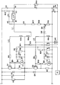
- the figure shows the circuit arrangement according to the preferred embodiment.
- This circuit arrangement is used to operate a T5 fluorescent lamp LP, which has an electrical power consumption (nominal power) of approximately 35 W.
- Appropriate dimensioning of the Electrical components of the preferred embodiment of the circuit arrangement according to the invention are given in the table.
- This circuit arrangement has a self-oscillating half-bridge inverter equipped with two npn bipolar transistors Q1, Q2.
- the half-bridge inverter is supplied with a DC voltage, which is obtained in the usual way by rectification from the grid voltage.
- a load circuit designed as a resonance circuit is connected to the output M of the half-bridge inverter. It contains the primary winding RKa of a toroidal transformer, a resonance inductor L1, the electrode filament E1 of the lamp LP, a resonance capacitor C1 and the electrode filament E2 of the fluorescent lamp LP.
- the discharge path of the low-pressure discharge lamp LP is connected in parallel to the resonance capacitor C1.
- the resonance capacitor C1 is also connected via the electrode coil E2 to the center tap V1 between the two coupling capacitors C2, C3, which in turn are arranged parallel to the half-bridge inverter Q1, Q2.
- the half-bridge inverter is controlled with the aid of the toroidal core transformer, the primary winding RKa of which is part of the load circuit and the secondary windings RKb, RKc are each arranged in a control circuit of the half-bridge inverter transistors Q1, Q2.
- the circuit arrangement has a starting device which essentially consists of the starting capacitor C5, the diac DC, the diode D3 and the ohmic resistors R2, R12, R13, R14.
- the two bipolar transistors Q1, Q2 of the half-bridge inverter are each equipped with a free-wheeling diode D1, D2, which are connected in parallel to the collector-emitter path of the corresponding transistor Q1, Q2.
- An ohmic resistor R1 and a capacitor C4 are arranged in parallel with the freewheeling diode D1. So far, the circuit arrangement corresponds to a self-oscillating, half-bridge inverter, such as that on pages 62-63 of the book Switching power supplies "by W. Hirschmann / A. Hauenstein, publisher Siemens AG.
- the control circuits of the two bipolar transistors Q1, Q2 each contain a basic series resistor R3 or R4, which is connected via an inductor L2 or L3 to the secondary winding RKb or RKc of the toroidal core transformer arranged in this control circuit.
- the emitter resistance of the bipolar transistor Q1 is formed by a parallel circuit consisting of the ohmic resistors R5, R6 and the auxiliary transistor T1. This parallel connection is designed such that the low-resistance resistor R6 is arranged in series with the drain-source path of the auxiliary transistor T1 and the higher-resistance resistor R5 is connected in parallel with this series circuit consisting of the resistor R6 and the drain-source path of the auxiliary transistor T1 .
- the emitter resistance of the bipolar transistor Q2 is formed by a parallel circuit consisting of the ohmic resistors R7, R8 and the auxiliary transistor T2.
- This parallel connection is also designed such that the low-resistance resistor R8 is arranged in series with the drain-source path of the auxiliary transistor T2 and the higher-resistance resistor R7 is connected in parallel with this series circuit consisting of the resistor R8 and the drain-source path of the auxiliary transistor T2 is.
- the control circuits of the two half-bridge inverter transistors Q1, Q2 also each have a base-emitter parallel resistor R9 or R10, which is connected in parallel to the base-emitter path of the corresponding bipolar transistor Q1, Q2 and improves the switching behavior of these two bipolar transistors Q1, Q2.
- the two auxiliary transistors T1, T2 are field effect transistors which are controlled with the aid of the control circuit IC.
- the purpose of the output of the control circuit IC is connected on the one hand via the ohmic resistor R11 and the diode D5 to the gate connection of the field effect transistor T1 and on the other hand via the ohmic resistor R21 to the gate connection of the field effect transistor T2.
- a capacitor C6 or C7 and an ohmic resistor R15 or R16 are connected in parallel to the gate of the field effect transistor T1 or T2.
- a Zener diode Z1, Z2 serving as overvoltage protection is arranged in parallel to the gate of each auxiliary transistor T1, T2.
- the circuit arrangement also has a voltage divider, which essentially consists of the resistors R17, R18 and R19.
- This voltage divider is connected via capacitor C8 and branch point V2 to a connection of resonance capacitor C1 and to a connection of lamp electrode E1, so that the voltage divider is connected in parallel with the resonance capacitor C1 in terms of alternating current.
- the center tap V3 between the resistors R18, R19 of the voltage divider is connected via a diode D6 and a Zener diode DZ to the gate terminal of the field effect transistor T2.
- the Zener diode DZ and the diode D6 are polarized in opposite directions.
- the starting capacitor C5 charges via the resistors R12, R13 to the breakdown voltage of the DC DC, which then generates trigger pulses for the base of the bipolar transistor Q2 and thereby causes the half-bridge inverter to oscillate.
- the start capacitor C5 is discharged via the resistor R2 and the diode D3 to such an extent that the diac DC does not generate any further trigger pulses.
- the two inverter transistors Q1, Q2 switch alternately, so that the center tap M of the half bridge is alternately connected to the positive or negative pole of the DC voltage supply.
- the taps M and V1 generates a medium-frequency alternating current in the load circuit designed as a series resonance circuit, the frequency of which corresponds to the clock frequency of the half-bridge inverter.
- the clock frequency of the half-bridge inverter is usually more than 20 kHz.
- the electronic components of the circuit arrangement according to the invention are also dimensioned such that the clock frequency of the self-oscillating half-bridge inverter is above the resonance frequency of the series resonance circuit L1, C1.
- the auxiliary transistors T1, T2 are initially in the blocked state, so that only the higher-impedance resistors R5 and R7 are effective as the emitter resistor for the bipolar transistors Q1, Q2.
- the control circuit IC switches its output voltage from approximately 0 V to approximately 10 V to 12 V, so that the control voltage for switching the field effect transistor T2 through the resistor R21 is built up on the capacitor C7.
- the discharge resistor R15 has a considerably larger resistance value than the charging resistor R11, the time constant of the capacitor C6 for the discharge process is considerably greater than for the charging process, so that the control voltage for the auxiliary transistor T1 required for switching through is still present at the capacitor C6 when the duty cycle of the bipolar transistor Q2 has already ended.
- the capacitor C6 is recharged via the resistor R11 and the diode D5.
- the effective emitter resistance for the bipolar transistors Q1 is given by the total or equivalent resistance of the resistors R5 and R6 which are now connected in parallel, if the resistance of the drain-source path of the auxiliary transistor T1 is disregarded.
- the effective emitter resistance of the bipolar transistor Q2 which essentially results from the equivalent resistance of the parallel resistors R7 and R8 when the auxiliary transistor T2 is switched on. Due to the now significantly lower effective emitter resistance of the bipolar transistors Q1, Q2 and the resulting reduced negative feedback of the half-bridge inverter, the clock frequency of the half-bridge inverter drops. The detuning between the clock frequency of the half-bridge inverter and the resonance frequency of the resonance circuit L1, C1 drops so far that the ignition voltage required to ignite the lamp LP is generated at the resonance capacitor C1 by the method of resonance increase.
- the then electrically conductive discharge path of the lamp LP constitutes a shunt to the resonance capacitor C1, so that only the operating voltage of the lamp LP drops via the resonance capacitor C1.
- the resonance circuit components C1, L1 are dimensioned in the preferred embodiment such that only a relatively small pin current flows through the electrodes E1, E2.
- the resonance circuit of the preferred embodiment therefore has a comparatively large resonance inductance L1 and a relatively high quality. Due to the high quality of the resonance circuit, a high voltage drop can build up on the resonance circuit components C1, L1.
- the voltage divider R17, R18, R19 together with the Zener diode DZ and the diode D6 now offers an additional possibility to limit or regulate the voltage drop in the resonance circuit C1, L1.
- the voltage drop across the resonance capacitor C1 or the lamp LP is detected by this voltage divider and divided down according to the resistance values of the ohmic resistors R17, R18, R19.
- the Zener diode DZ remains and thus also the current path, which starts from the gate of the field effect transistor T2 via the Zener diode DZ and the resistor R19 leads to the negative pole of the DC voltage source, de-energized and the field effect transistor T2 maintains its full control signal.
- the amplitude of the resonance capacitor voltage reaches this critical value, the voltage drop between the gate of the field effect transistor T2 and the branch point increases when the negative half-wave of the resonance capacitor voltage passes through V3 so far that the Zener diode DZ becomes conductive.
- the gate of the field effect transistor T2 only receives a reduced control signal since part of the control signal coming from the control circuit IC flows through the now conductive zener diode DZ and the voltage divider resistor R19 to the negative pole of the DC voltage source.
- the rectifier diode D6 is polarized so that the Zener diode DZ is only sensitive to the negative half-wave of the resonant capacitor voltage.
- a reduced control signal for the gate of the field effect transistor T2 reduces the conductivity of the drain-source path of the field effect transistor T2 and thus increases the effective emitter resistance of the bipolar transistor Q2.
- the effective emitter resistance of the bipolar transistor Q2 is calculated from the no longer negligible resistance of the drain-source path of the auxiliary transistor T2 and the resistance values of the ohmic resistors R7 and R8. This increase in the effective emitter resistance of the transistor Q2 causes a shortened on-time of the bipolar transistor Q2 and increases the clock frequency of the half-bridge inverter accordingly, whereby the open circuit voltage at the resonance capacitor is reduced.
- the invention is not limited to the exemplary embodiment explained in more detail above.
- the circuit arrangement according to the invention can also be used for dimming the lamp LP.
- the control circuit IC is to be designed in such a way that it not only switches between two voltage stages 0 V and 12 V for driving the auxiliary transistors T1, T2, as described in the exemplary embodiment above, but also provides a continuously variable output voltage after the lamp has been ignited .
Landscapes
- Circuit Arrangements For Discharge Lamps (AREA)
Applications Claiming Priority (2)
| Application Number | Priority Date | Filing Date | Title |
|---|---|---|---|
| DE19613149 | 1996-04-03 | ||
| DE19613149A DE19613149A1 (de) | 1996-04-03 | 1996-04-03 | Schaltungsanordnung zum Betrieb elektrischer Lampen |
Publications (3)
| Publication Number | Publication Date |
|---|---|
| EP0800335A2 true EP0800335A2 (fr) | 1997-10-08 |
| EP0800335A3 EP0800335A3 (fr) | 1999-05-06 |
| EP0800335B1 EP0800335B1 (fr) | 2002-11-27 |
Family
ID=7790253
Family Applications (1)
| Application Number | Title | Priority Date | Filing Date |
|---|---|---|---|
| EP97104699A Expired - Lifetime EP0800335B1 (fr) | 1996-04-03 | 1997-03-19 | Circuit pour alimenter des lampes électriques |
Country Status (4)
| Country | Link |
|---|---|
| US (1) | US5831396A (fr) |
| EP (1) | EP0800335B1 (fr) |
| CA (1) | CA2201537C (fr) |
| DE (2) | DE19613149A1 (fr) |
Families Citing this family (27)
| Publication number | Priority date | Publication date | Assignee | Title |
|---|---|---|---|---|
| DE19709545A1 (de) * | 1997-03-07 | 1998-09-10 | Patent Treuhand Ges Fuer Elektrische Gluehlampen Mbh | Schaltsteuerung einer Betriebsschaltung |
| US6188553B1 (en) | 1997-10-10 | 2001-02-13 | Electro-Mag International | Ground fault protection circuit |
| US6020688A (en) | 1997-10-10 | 2000-02-01 | Electro-Mag International, Inc. | Converter/inverter full bridge ballast circuit |
| US6069455A (en) * | 1998-04-15 | 2000-05-30 | Electro-Mag International, Inc. | Ballast having a selectively resonant circuit |
| US6091288A (en) * | 1998-05-06 | 2000-07-18 | Electro-Mag International, Inc. | Inverter circuit with avalanche current prevention |
| US6028399A (en) * | 1998-06-23 | 2000-02-22 | Electro-Mag International, Inc. | Ballast circuit with a capacitive and inductive feedback path |
| US6100645A (en) * | 1998-06-23 | 2000-08-08 | Electro-Mag International, Inc. | Ballast having a reactive feedback circuit |
| US6107750A (en) * | 1998-09-03 | 2000-08-22 | Electro-Mag International, Inc. | Converter/inverter circuit having a single switching element |
| US6160358A (en) * | 1998-09-03 | 2000-12-12 | Electro-Mag International, Inc. | Ballast circuit with lamp current regulating circuit |
| US6181082B1 (en) | 1998-10-15 | 2001-01-30 | Electro-Mag International, Inc. | Ballast power control circuit |
| US6169375B1 (en) | 1998-10-16 | 2001-01-02 | Electro-Mag International, Inc. | Lamp adaptable ballast circuit |
| US6137233A (en) * | 1998-10-16 | 2000-10-24 | Electro-Mag International, Inc. | Ballast circuit with independent lamp control |
| US6181083B1 (en) | 1998-10-16 | 2001-01-30 | Electro-Mag, International, Inc. | Ballast circuit with controlled strike/restart |
| US6222326B1 (en) | 1998-10-16 | 2001-04-24 | Electro-Mag International, Inc. | Ballast circuit with independent lamp control |
| US6127786A (en) * | 1998-10-16 | 2000-10-03 | Electro-Mag International, Inc. | Ballast having a lamp end of life circuit |
| US6100648A (en) * | 1999-04-30 | 2000-08-08 | Electro-Mag International, Inc. | Ballast having a resonant feedback circuit for linear diode operation |
| US7592753B2 (en) * | 1999-06-21 | 2009-09-22 | Access Business Group International Llc | Inductively-powered gas discharge lamp circuit |
| AU6335400A (en) | 1999-07-02 | 2001-01-22 | Fusion Lighting, Inc. | High output lamp with high brightness |
| DE19933161A1 (de) * | 1999-07-20 | 2001-01-25 | Patent Treuhand Ges Fuer Elektrische Gluehlampen Mbh | Schaltungsanordnung |
| DE10140723A1 (de) | 2001-08-27 | 2003-03-20 | Patent Treuhand Ges Fuer Elektrische Gluehlampen Mbh | Betriebsschaltung für Entladungslampe mit vorheizbaren Elektroden |
| WO2003030595A1 (fr) * | 2001-10-01 | 2003-04-10 | Koninklijke Philips Electronics N.V. | Circuit en pont auto-oscillant comprenant un circuit de demarrage |
| DE10206731B4 (de) * | 2002-02-18 | 2016-12-22 | Tridonic Gmbh & Co Kg | Lampensensor für ein Vorschaltgerät zum Betrieb einer Gasentladunslampe |
| DE10235217A1 (de) * | 2002-08-01 | 2004-02-19 | Patent-Treuhand-Gesellschaft für elektrische Glühlampen mbH | Schaltungsvorrichtung und Verfahren zum Betreiben einer Lampe |
| US7821208B2 (en) * | 2007-01-08 | 2010-10-26 | Access Business Group International Llc | Inductively-powered gas discharge lamp circuit |
| US7755296B2 (en) * | 2007-03-19 | 2010-07-13 | System General Corp. | Resonant inverter |
| CN101926085A (zh) * | 2008-01-24 | 2010-12-22 | 欧陆汽车系统美国有限公司 | 多级开关电源 |
| DE102014107991B4 (de) * | 2014-06-05 | 2020-01-30 | Krohne Messtechnik Gmbh | Feldgerät mit Schaltwandlerschaltung |
Family Cites Families (5)
| Publication number | Priority date | Publication date | Assignee | Title |
|---|---|---|---|---|
| NL8201631A (nl) * | 1982-04-20 | 1983-11-16 | Philips Nv | Gelijkstroom-wisselstroomomzetter voor het ontsteken en met wisselstroom voeden van een gas- en/of dampontladingslamp. |
| DD267617A1 (de) * | 1987-11-16 | 1989-05-03 | Narva Rosa Luxemburg K | Schaltungsanordnung eines halbbrueckenwechselrichters |
| CA1318345C (fr) * | 1988-04-13 | 1993-05-25 | David J. Cockram | Dispositif d'allumage pour lampe a decharge |
| US5097183A (en) * | 1991-06-25 | 1992-03-17 | Led Corporation N.V. | Master-slave half-bridge DC-to-AC switchmode power converter |
| DE9114039U1 (de) * | 1991-11-12 | 1992-01-09 | Patent-Treuhand-Gesellschaft für elektrische Glühlampen mbH, 8000 München | Schaltungsanordnung zum Betrieb einer oder mehrerer Niederdruckentladungslampen |
-
1996
- 1996-04-03 DE DE19613149A patent/DE19613149A1/de not_active Withdrawn
-
1997
- 1997-03-19 DE DE59708791T patent/DE59708791D1/de not_active Expired - Lifetime
- 1997-03-19 EP EP97104699A patent/EP0800335B1/fr not_active Expired - Lifetime
- 1997-03-31 US US08/828,983 patent/US5831396A/en not_active Expired - Fee Related
- 1997-04-02 CA CA002201537A patent/CA2201537C/fr not_active Expired - Fee Related
Also Published As
| Publication number | Publication date |
|---|---|
| DE59708791D1 (de) | 2003-01-09 |
| DE19613149A1 (de) | 1997-10-09 |
| EP0800335B1 (fr) | 2002-11-27 |
| CA2201537A1 (fr) | 1997-10-03 |
| EP0800335A3 (fr) | 1999-05-06 |
| US5831396A (en) | 1998-11-03 |
| CA2201537C (fr) | 2004-09-14 |
Similar Documents
| Publication | Publication Date | Title |
|---|---|---|
| EP0800335B1 (fr) | Circuit pour alimenter des lampes électriques | |
| EP0798952B1 (fr) | Circuit pour l'opération de lampes électriques et procédé d'opération | |
| EP0264765A2 (fr) | Disposition de circuit pour la mise en oeuvre de lampe à incandescence halogène basse tension | |
| WO1993012631A1 (fr) | Circuit pour actionner une ou plusieurs lampe(s) a decharge a basse pression | |
| DE19653604A1 (de) | Vorschaltung für eine Leuchtstofflampe | |
| EP0693864B1 (fr) | Circuit pour alimenter une ou plusieurs lampes à décharge basse-pression | |
| DE69315761T2 (de) | Geschützter Umrichter zur Steuerung einer Entladungslampe | |
| EP0439240B1 (fr) | Ballast électronique | |
| EP0655880B1 (fr) | Circuit basse tension pour l'alimentation d'une lampe à décharge basse pression | |
| DE69202783T2 (de) | Zünd- und Betriebsschaltung für Bogenentladungslampe. | |
| EP1033066A1 (fr) | Circuit pour actionner au moins une lampe a decharge | |
| EP0753987B1 (fr) | Circuit et procédé d'opération de lampes électriques | |
| DE69207215T2 (de) | Vielseitiges elektronisches Vorschaltgerät | |
| DE69616451T2 (de) | Umschaltanordnung | |
| DE3530638A1 (de) | Schaltungsanordnung zum starten und betrieb von gasentladungslampen | |
| EP0648068B1 (fr) | Circuit d'alimentation de lampes électriques | |
| EP0519220A1 (fr) | Ballast avec temps de chauffage commandé | |
| DE3504803A1 (de) | Gegentaktgenerator | |
| DE3626209A1 (de) | Vorschaltgeraet fuer wenigstens eine entladungslampe | |
| EP0155729B1 (fr) | Circuit pour l'exploitation à courant alternatif pour lampes à décharge à haute pression | |
| DE69714163T2 (de) | Schaltungsanordnung | |
| EP0276460A1 (fr) | Disposition de circuit pour mettre en oeuvre une lampe à décharge basse pression | |
| EP0021508A1 (fr) | Circuit d'allumage et de commande pour lampes à décharge dans un gaz et/ou une vapeur | |
| EP1395094A1 (fr) | Appareil et procédé permettant de faire fonctionner une lampe | |
| EP2140735B1 (fr) | Ensemble circuit servant à amorcer et à faire fonctionner au moins une lampe à décharge |
Legal Events
| Date | Code | Title | Description |
|---|---|---|---|
| PUAI | Public reference made under article 153(3) epc to a published international application that has entered the european phase |
Free format text: ORIGINAL CODE: 0009012 |
|
| AK | Designated contracting states |
Kind code of ref document: A2 Designated state(s): BE DE FR GB IT NL SE |
|
| PUAL | Search report despatched |
Free format text: ORIGINAL CODE: 0009013 |
|
| AK | Designated contracting states |
Kind code of ref document: A3 Designated state(s): BE DE FR GB IT NL SE |
|
| 17P | Request for examination filed |
Effective date: 19990607 |
|
| 17Q | First examination report despatched |
Effective date: 20010625 |
|
| GRAG | Despatch of communication of intention to grant |
Free format text: ORIGINAL CODE: EPIDOS AGRA |
|
| GRAG | Despatch of communication of intention to grant |
Free format text: ORIGINAL CODE: EPIDOS AGRA |
|
| GRAH | Despatch of communication of intention to grant a patent |
Free format text: ORIGINAL CODE: EPIDOS IGRA |
|
| GRAH | Despatch of communication of intention to grant a patent |
Free format text: ORIGINAL CODE: EPIDOS IGRA |
|
| GRAA | (expected) grant |
Free format text: ORIGINAL CODE: 0009210 |
|
| AK | Designated contracting states |
Kind code of ref document: B1 Designated state(s): BE DE FR GB IT NL SE |
|
| REG | Reference to a national code |
Ref country code: GB Ref legal event code: FG4D Free format text: NOT ENGLISH |
|
| RIC1 | Information provided on ipc code assigned before grant |
Free format text: 7H 05B 41/292 A, 7H 05B 41/38 B |
|
| REF | Corresponds to: |
Ref document number: 59708791 Country of ref document: DE Date of ref document: 20030109 |
|
| GBT | Gb: translation of ep patent filed (gb section 77(6)(a)/1977) |
Effective date: 20030226 |
|
| ET | Fr: translation filed | ||
| PLBE | No opposition filed within time limit |
Free format text: ORIGINAL CODE: 0009261 |
|
| STAA | Information on the status of an ep patent application or granted ep patent |
Free format text: STATUS: NO OPPOSITION FILED WITHIN TIME LIMIT |
|
| 26N | No opposition filed |
Effective date: 20030828 |
|
| PGFP | Annual fee paid to national office [announced via postgrant information from national office to epo] |
Ref country code: NL Payment date: 20060308 Year of fee payment: 10 |
|
| PGFP | Annual fee paid to national office [announced via postgrant information from national office to epo] |
Ref country code: BE Payment date: 20060314 Year of fee payment: 10 |
|
| PGFP | Annual fee paid to national office [announced via postgrant information from national office to epo] |
Ref country code: FR Payment date: 20060324 Year of fee payment: 10 |
|
| PGFP | Annual fee paid to national office [announced via postgrant information from national office to epo] |
Ref country code: IT Payment date: 20060331 Year of fee payment: 10 |
|
| PG25 | Lapsed in a contracting state [announced via postgrant information from national office to epo] |
Ref country code: SE Free format text: LAPSE BECAUSE OF NON-PAYMENT OF DUE FEES Effective date: 20070320 |
|
| EUG | Se: european patent has lapsed | ||
| GBPC | Gb: european patent ceased through non-payment of renewal fee |
Effective date: 20070319 |
|
| NLV4 | Nl: lapsed or anulled due to non-payment of the annual fee |
Effective date: 20071001 |
|
| BERE | Be: lapsed |
Owner name: *PATENT-TREUHAND-G.- FUR ELEKTRISCHE GLUHLAMPEN M. Effective date: 20070331 |
|
| PG25 | Lapsed in a contracting state [announced via postgrant information from national office to epo] |
Ref country code: BE Free format text: LAPSE BECAUSE OF NON-PAYMENT OF DUE FEES Effective date: 20070331 |
|
| REG | Reference to a national code |
Ref country code: FR Ref legal event code: ST Effective date: 20071130 |
|
| PG25 | Lapsed in a contracting state [announced via postgrant information from national office to epo] |
Ref country code: NL Free format text: LAPSE BECAUSE OF NON-PAYMENT OF DUE FEES Effective date: 20071001 |
|
| PGFP | Annual fee paid to national office [announced via postgrant information from national office to epo] |
Ref country code: SE Payment date: 20060308 Year of fee payment: 10 |
|
| PG25 | Lapsed in a contracting state [announced via postgrant information from national office to epo] |
Ref country code: GB Free format text: LAPSE BECAUSE OF NON-PAYMENT OF DUE FEES Effective date: 20070319 |
|
| PG25 | Lapsed in a contracting state [announced via postgrant information from national office to epo] |
Ref country code: FR Free format text: LAPSE BECAUSE OF NON-PAYMENT OF DUE FEES Effective date: 20070402 |
|
| PGFP | Annual fee paid to national office [announced via postgrant information from national office to epo] |
Ref country code: GB Payment date: 20060308 Year of fee payment: 10 |
|
| PG25 | Lapsed in a contracting state [announced via postgrant information from national office to epo] |
Ref country code: IT Free format text: LAPSE BECAUSE OF NON-PAYMENT OF DUE FEES Effective date: 20070319 |
|
| REG | Reference to a national code |
Ref country code: DE Ref legal event code: R081 Ref document number: 59708791 Country of ref document: DE Owner name: OSRAM GMBH, DE Free format text: FORMER OWNER: OSRAM GESELLSCHAFT MIT BESCHRAENKTER HAFTUNG, 81543 MUENCHEN, DE Effective date: 20111130 |
|
| PG25 | Lapsed in a contracting state [announced via postgrant information from national office to epo] |
Ref country code: DE Free format text: LAPSE BECAUSE OF NON-PAYMENT OF DUE FEES Effective date: 20111001 |
|
| REG | Reference to a national code |
Ref country code: DE Ref legal event code: R084 Ref document number: 59708791 Country of ref document: DE Effective date: 20120417 |
|
| REG | Reference to a national code |
Ref country code: DE Ref legal event code: R081 Ref document number: 59708791 Country of ref document: DE Owner name: OSRAM GMBH, DE Free format text: FORMER OWNER: OSRAM AG, 81543 MUENCHEN, DE Effective date: 20130205 |
|
| PGFP | Annual fee paid to national office [announced via postgrant information from national office to epo] |
Ref country code: DE Payment date: 20130321 Year of fee payment: 17 |
|
| REG | Reference to a national code |
Ref country code: DE Ref legal event code: R081 Ref document number: 59708791 Country of ref document: DE Owner name: OSRAM GMBH, DE Free format text: FORMER OWNER: OSRAM GMBH, 81543 MUENCHEN, DE Effective date: 20130822 |
|
| REG | Reference to a national code |
Ref country code: DE Ref legal event code: R119 Ref document number: 59708791 Country of ref document: DE |
|
| REG | Reference to a national code |
Ref country code: DE Ref legal event code: R119 Ref document number: 59708791 Country of ref document: DE Effective date: 20141001 |
|
| PG25 | Lapsed in a contracting state [announced via postgrant information from national office to epo] |
Ref country code: DE Free format text: LAPSE BECAUSE OF NON-PAYMENT OF DUE FEES Effective date: 20141001 |