EP0800722B1 - Circuit d'attaque cmos - Google Patents
Circuit d'attaque cmos Download PDFInfo
- Publication number
- EP0800722B1 EP0800722B1 EP96933564A EP96933564A EP0800722B1 EP 0800722 B1 EP0800722 B1 EP 0800722B1 EP 96933564 A EP96933564 A EP 96933564A EP 96933564 A EP96933564 A EP 96933564A EP 0800722 B1 EP0800722 B1 EP 0800722B1
- Authority
- EP
- European Patent Office
- Prior art keywords
- circuit
- output
- coupled
- timing
- terminal
- Prior art date
- Legal status (The legal status is an assumption and is not a legal conclusion. Google has not performed a legal analysis and makes no representation as to the accuracy of the status listed.)
- Expired - Lifetime
Links
- 230000007704 transition Effects 0.000 description 4
- 238000010586 diagram Methods 0.000 description 2
- 230000004913 activation Effects 0.000 description 1
- 239000003990 capacitor Substances 0.000 description 1
- 230000008878 coupling Effects 0.000 description 1
- 238000010168 coupling process Methods 0.000 description 1
- 238000005859 coupling reaction Methods 0.000 description 1
- 230000009849 deactivation Effects 0.000 description 1
- 230000009977 dual effect Effects 0.000 description 1
Images


Classifications
-
- H—ELECTRICITY
- H03—ELECTRONIC CIRCUITRY
- H03K—PULSE TECHNIQUE
- H03K5/00—Manipulating of pulses not covered by one of the other main groups of this subclass
- H03K5/01—Shaping pulses
- H03K5/04—Shaping pulses by increasing duration; by decreasing duration
- H03K5/06—Shaping pulses by increasing duration; by decreasing duration by the use of delay lines or other analogue delay elements
-
- H—ELECTRICITY
- H03—ELECTRONIC CIRCUITRY
- H03K—PULSE TECHNIQUE
- H03K19/00—Logic circuits, i.e. having at least two inputs acting on one output; Inverting circuits
- H03K19/0008—Arrangements for reducing power consumption
- H03K19/0013—Arrangements for reducing power consumption in field effect transistor circuits
Definitions
- the invention relates to a CMOS driver circuit having an input terminal and an output terminal, and comprising:
- CMOS driver circuit is known from US 5,317,206.
- Standard CMOS drivers having a circuit configuration such as that shown by transistors 100 and 102 in Fig. 1, are normally quite adequate for driving relatively large off-chip capacitive loads, such as the gate of a power transistor.
- relatively large off-chip capacitive loads such as the gate of a power transistor.
- VCC power supply terminal
- ground common terminal
- CMOS drivers are typically limited to low-frequency (i.e., below about 100 KHz) applications and smaller drivers.
- the two CMOS driver transistors can be provided with separate gate drive signals. Then, by using a timing circuit, it can be ensured that there will be a slight time delay between activation of one transistor of the CMOS pair and deactivation of the other transistor, so that both transistors will never be on simultaneously, thus substantially preventing shoot-through current from flowing between the power supply terminal and ground.
- CMOS predriver circuits can be used to boost the driving capability of the timing circuit to drive the output driver stage.
- the predrivers themselves can be quite large, and, if conventional CMOS stages are used as predrivers, significant shoot-through power will be dissipated in the predrivers during transitions.
- the maximum operating frequency of prior-art CMOS driver circuits is still limited by shoot-through dissipation to about 1 MHz.
- the invention aims to provide a CMOS driver circuit capable of driving relatively large off-chip capacitive loads (in the range of 1 to 2 nF), such as the gate of a power transistor, at frequencies in the range of several MHz without dissipating significant power due to shoot-through current.
- a CMOS driver circuit as mentioned in the opening paragraph is according to the invention characterized in that the pulses of each timing signal have different pulsewidths than the pulses of the other timing signals and in that the pulses of the three different timing signals have mutually-different starting and ending time points with reference to a common input signal VIN at the input terminal of the CMOS driver circuit, such that no transistor of a series-connected pair will turn on before its associated transistor turns off.
- the CMOS driver circuit according to the invention has two levels of zero-shoot-through drivers (dual predrivers and an output driver) which are controlled by a timing circuit which provides three different timing signals to the predriver stages (and through the predriver stages to the output driver), with the three timing signals having differing waveforms the CMOS driver circuit could be operated while substantially eliminating shoot-through-power dissipation in the circuit.
- said first timing signal comprises a first pulse having a first pulse width
- said second timing signal comprises a second pulse having a second pulsewidth greater than said first pulse width
- said third timing signal comprises a third pulse having a third pulse width greater than said second pulsewidth.
- the three different timing signals are substantially square-wave pulses.
- the timing signals may differ from each other by having at least one of a different rise time and a different fall time.
- the timing circuit includes three CMOS inverter circuits, with current sources inserted in selected ones of the CMOS inverter circuits to provide the different rise and/or fall times for the three timing signals.
- the timing circuit may be implemented digitally, by a circuit using a combination of AND and OR gates and delay elements, in which case the three timing signals will be substantially square-wave signals having different pulsewidths.
- CMOS driver circuits configured in accordance with the invention are capable of driving relatively large off-chip capacitive loads at high frequencies without significant shoot-through power dissipation.
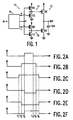
- a CMOS driver circuit 10 in accordance with the invention is shown in Fig. 1.
- the driver circuit 10 includes an output driver circuit stage 12 having a PMOS transistor 100 and an NMOS transistor 102 having their main current paths coupled in series between a power supply terminal V CC and ground, with a common connection between the main current paths forming an output terminal OUT of the CMOS driver circuit 10.
- a capacitor 104 is shown connected between the output terminal and ground by a dashed line to represent the capacitance of an external load such as the gate capacitance of a power transistor being driven by the CMOS driver circuit.
- the CMOS driver circuit 10 also includes first and second predriver circuits 14 and 18 having PMOS transistors 106 and 108 and NMOS transistors 110 and 112, respectively, with each pair of PMOS and NMOS transistors being coupled in series between V CC and ground.
- a common connection between the main current paths of each pair of PMOS and NMOS transistors, at points d and e, respectively, is coupled to the gate electrode of a corresponding output driver circuit transistor 100 or 102.
- the CMOS driver circuit 10 also includes a timing circuit 16, shown in Fig. 1 in block-diagram form, having an input terminal IN and three output terminals a, b, and c.
- the timing circuit is coupled to the two predriver circuits by coupling output terminal a to the gate of transistor 110, output terminal b to the gates of transistors 106 and 112, and output terminal c to the gate of transistor 108.
- the timing circuit 16 of Fig. 1 may be implemented in several ways, two of which are illustrated in Figs. 3 and 5.
- input terminal IN is coupled to OR gates 300 and 302, and AND gate 304.
- the outputs of gates 302 and 304 are coupled to delay ( ⁇ ) elements 306 and 308, respectively, and the outputs of these delay elements are cross-coupled back to second inputs of the gates 302 and 304.
- the output of delay element 306 is also coupled to a delay element 310, the output of which is in turn coupled to a second input of OR gate 300.
- the output of OR gate 300 forms timing circuit output c, with the output of delay element 306 forming timing circuit output terminal b and the output of delay element 308 forming the output terminal a of the timing circuit.
- timing circuit 16 includes first, second and third CMOS inverter circuits 500, 502 and 504, with each CMOS inverter circuit being composed of series-connected PMOS and NMOS transistors 506, 508; 510, 512; and 514; 516; respectively.
- the input terminal IN of the timing circuit 16 is coupled to the gate electrodes of transistors 506, 508, 510, 512, 514 and 516, and the output terminals of inverters 500, 502 and 504 are coupled to terminals a, b and c, respectively.
- Inverter circuits 500 and 504 further include current sources 518 connected between Vcc and transistor 506, and current source 520 connected between transistor 516 and ground, respectively.
- CMOS driver circuit 10 of Fig. 1 and the timing circuits 16 of Fig. 3 and Fig. 5 may be better understood with reference to the signal timing diagrams of Figs. 2a-f, 4a-d and 6a-d, respectively.
- Figs. 2a, 2b and 2c show representative waveforms at output terminals a, b and c of timing circuit 16.
- these three pulse waveforms have mutually-different starting (t1, t2 and t3) and ending (t4, t5 and t6) time points with reference to a common input signal V IN at terminal IN.
- the waveforms of Figs. 2a-2c are applied to the predriver circuits 14 and 18, the waveforms shown in Figs.
- transistor 110 in Fig. 1 is turned on when the waveform in Fig. 2a goes high, at time t3, and is turned off when that waveform goes low at time t4.
- Transistor 106 connected in series with transistor 110, turns off when its gate voltage (Vb in Fig. 2b) goes high, at time t2, and turns back on at time t5 when Vb goes low. Since t2 is slightly earlier than t3, and t5 is slightly later than t4, there is no point in time when both transistors will be on simultaneously. The same relationship applies with respect to the two transistors of predriver circuit 18, since waveforms Vb and Vc have a similar timing relationship to that of Va and Vb, as shown in Figs. 2b and 2c.
- the waveforms Vd and Ve are generated at the outputs of the predriver circuits and are applied to the gates of transistors 100 and 102, respectively, of the output driver circuit 12.
- the output waveform Vour will be generated at the output terminal OUT as shown in Fig. 2f.
- transistor 102 will be turned off at t2, before transistor 100 is turned on at time t3, and similarly, transistor 100 will be turned off at time t5, before transistor 102 is turned on at time t6, thus substantially preventing unwanted shoot-through dissipation in the output driver stage.
- the circuit of the invention controls the turn-on and turn-off timing of six transistors with only three independently-generated timing signals (Va, Vb and Vc), thus offering substantially improved performance in a relatively simple and economical circuit. This is accomplished both by using the same signal Vb in both predrivers, and by deriving the timing signals for the output driver circuit from the predriver circuit outputs, Vd and Ve, without using separate timing circuitry for the output driver circuit.
- the present invention enables the use of a total of only three different properly-timed input waveforms (instead of the six that would be conventionally required) to activate the two predriver circuits and the output driver circuit with substantially no shoot-through power dissipation, thus resulting in a cost-effective implementation of a low-power high-frequency CMOS driver circuit.
- Figs. 3 and 5 Two different implementations of the timing circuit 16, as previously described, are shown in Figs. 3 and 5.
- the "digital" implementation of Fig. 3 uses logic gates and delay elements in order to generate the output waveforms Va, Vb and Vc from the input waveform V IN as shown in Figs. 4a-4d with the AND and OR gates and the delay elements each operating in a conventional manner familiar to those of ordinary skill in this art and therefore not described in further detail here.
- the logic gates, in combination with the delay elements in the circuit of Fig. 3 enable the generation of three waveforms Va, Vb and Vc having a pyramid-shaped timing relationship as shown in Figs.
- V IN having a pulsewidth of (t4-t1)
- Va having a pulsewidth of (t5-t3)
- Vb having a pulsewidth of (t6-t2)
- Vc having a pulsewidth of (t7-t1).
- the relative timing of the three timing circuit output signals Va, Vb and Vc is obtained by inserting current sources 518 and 520 into the first and third CMOS inverter circuits 500 and 504, as shown in Fig. 5.
- the purpose of these current sources is to cause the leading or trailing edges of the pulses generated by the associated CMOS inverter to have a relatively more gradual rise or fall time than in a comparable CMOS inverter circuit without such a current source.
- V IN as shown in Fig.
- the output of the second CMOS inverter circuit 502 is shown as having a moderate rise time (t3-t1) and a moderate fall time (t7-t5).
- First CMOS inverter circuit 501 has an extended rise time (t4-t1) and a faster fall time (t5) due to the presence of current source 518 in the turn-on current path, and similarly, third CMOS inverter circuit 504 has a relatively fast rise time (t1) and an extended fall time (t8-t5) due to the presence of current source 520 in the turn-off path of the inverter circuit.
- waveform Va has an effective pulsewidth (t5-t3) which is less than the effective pulsewidth of waveform Vb (t6-t2), and the effective pulsewidth of waveform Vc (t7-t1) is greater than the pulsewidth of waveform Vb.
- both the rise time and the fall time of the waveform Vb, generated by the second CMOS inverter 502 which has no current source, is shown as having moderate rise and fall times, shown for illustration as approximately half way between the fast and slow rise and/or fall times of the waveforms Va and Vc.
- the circuit of Fig. 5 generates three different timing signals analogous to those shown in Figs. 2a-2c and 4b-4d.
- the present invention provides a CMOS driver circuit capable of driving relatively large off-chip capacitive loads at high frequencies in the range of several MHz. Additionally, the invention provides a CMOS driver circuit capable of driving relatively large capacitive loads at high frequencies without significant shoot-through power dissipation.
Landscapes
- Physics & Mathematics (AREA)
- Engineering & Computer Science (AREA)
- Computer Hardware Design (AREA)
- Computing Systems (AREA)
- General Engineering & Computer Science (AREA)
- Mathematical Physics (AREA)
- Nonlinear Science (AREA)
- Logic Circuits (AREA)
- Electronic Switches (AREA)
- Manipulation Of Pulses (AREA)
Claims (6)
- Circuit d'attaque CMOS possédant une borne d'entrée et une borne de sortie et comprenant :un circuit d'attaque de sortie possédant des premier et deuxième transistors MOS des premier et second types respectifs et ayant leurs voies de courant principales couplées en série entre une borne d'alimentation électrique et une borne commune, une connexion commune entre les voies de courant principales desdits premier et deuxième transistors MOS comprenant la borne de sortie dudit circuit d'attaque CMOS;un premier précircuit d'attaque possédant des troisième et quatrième transistors MOS desdits premier et deuxième types respectifs et comportant leurs voies de courant principales couplées en série entre ladite borne d'alimentation électrique et ladite borne commune, une connexion commune entre les voies de courant principales desdits troisième et quatrième transistors MOS étant couplée à une électrode de commande dudit premier transistor MOS;un deuxième précircuit d'attaque possédant des cinquième et sixième transistors MOS desdits premier et deuxième types respectifs et comportant leurs voies de courant principales couplées en série entre ladite borne d'alimentation électrique et ladite borne commune, une connexion commune entre les principales voies de courant desdits cinquième et sixième transistors MOS étant couplée à une électrode de commande dudit deuxième transistor MOS etun circuit de temporisation possédant une borne d'entrée qui comprend la borne d'entrée dudit circuit d'attaque CMOS et des première, deuxième et troisième bornes de sortie pour fournir différents premier, deuxième et troisième signaux de temporisation à une électrode de commande desdits quatrième, troisième, sixième et cinquième transistors MOS respectifs, lesdits signaux de temporisation comprenant des impulsions,
caractérisé en ce que les impulsions de chaque signal de temporisation ont des largeurs d'impulsion différentes des autres signaux de temporisation et en ce que les impulsions des trois signaux de temporisation différents ont des points temporels de début et de fin réciproquement différents par référence à un signal d'entrée commun VIN à la borne d'entrée du circuit d'attaque CMOS de telle sorte qu'aucun transistor d'une paire montée en série ne se mette en route avant que son transistor associé ne soit éteint. - Circuit d'attaque CMOS selon la revendication 1 dans lequel les impulsions de chaque signal de temporisation sont essentiellement des impulsions rectangulaires.
- Circuit d'attaque CMOS selon la revendication 1 dans lequel les impulsions de chaque signal de temporisation ont au moins un temps de croissance différent et un temps de décroissance différent des impulsions des autres signaux de temporisation.
- Circuit d'attaque CMOS selon la revendication 3, dans lequel ledit circuit de temporisation comprend des premier, deuxième et troisièmes circuits inverseurs CMOS couplés chacun entre ladite borne d'alimentation électrique et ladite borne commune, une entrée de chaque circuit inverseur étant couplée à la borne d'entrée dudit circuit de temporisation et une borne de sortie des premier, deuxième et troisième circuits inverseurs CMOS étant raccordée respectivement à des première, deuxième et troisième borne de sortie dudit circuit de temporisation, une première source de courant étant couplée entre une voie de courant principale dudit premier circuit inverseur CMOS et ladite borne d'alimentation électrique et une deuxième source de courant étant couplée entre une voie de courant principale dudit troisième circuit inverseur CMOS et ladite borne commune.
- Circuit d'attaque CMOS selon une ou plusieurs des revendications précédentes, dans lequel ledit premier signal de temporisation comprend une première impulsion possédant une première largeur d'impulsion, ledit deuxième signal de temporisation comprenant une deuxième impulsion ayant une deuxième largeur d'impulsion supérieure à ladite première largeur d'impulsion et ledit troisième signal de temporisation comprend une troisième impulsion possédant une troisième largeur d'impulsion supérieure à ladite deuxième largeur d'impulsion.
- Circuit d'attaque CMOS selon la revendication 5, dans lequel ledit circuit de temporisation comprend des première et deuxième grilles OU et une grille ET, chacune possédant une première entrée couplée à la borne d'entrée dudit circuit de temporisation, un premier circuit retardateur ayant une entrée couplée à une sortie de ladite première grille OU, un deuxième circuit retardateur ayant une entrée couplée à une sortie dudit premier circuit retardateur et une sortie couplée à une deuxième entrée de ladite deuxième grille OU et un troisième circuit retardateur ayant une entrée couplée à une sortie de ladite grille ET et une sortie couplée à une deuxième entrée de ladite première grille ET, la sortie dudit premier circuit retardateur étant couplée à une deuxième entrée de ladite grille ET et la sortie dudit troisième circuit retardateur à la sortie dudit premier circuit retardateur et une sortie de la deuxième grille OU comprend respectivement les premier, deuxième et troisième bornes de sortie du circuit de temporisation.
Applications Claiming Priority (3)
| Application Number | Priority Date | Filing Date | Title |
|---|---|---|---|
| US550129 | 1995-10-27 | ||
| US08/550,129 US5621342A (en) | 1995-10-27 | 1995-10-27 | Low-power CMOS driver circuit capable of operating at high frequencies |
| PCT/IB1996/001119 WO1997015981A1 (fr) | 1995-10-27 | 1996-10-18 | Circuit d'attaque cmos |
Publications (2)
| Publication Number | Publication Date |
|---|---|
| EP0800722A1 EP0800722A1 (fr) | 1997-10-15 |
| EP0800722B1 true EP0800722B1 (fr) | 2006-01-25 |
Family
ID=24195869
Family Applications (1)
| Application Number | Title | Priority Date | Filing Date |
|---|---|---|---|
| EP96933564A Expired - Lifetime EP0800722B1 (fr) | 1995-10-27 | 1996-10-18 | Circuit d'attaque cmos |
Country Status (7)
| Country | Link |
|---|---|
| US (1) | US5621342A (fr) |
| EP (1) | EP0800722B1 (fr) |
| JP (1) | JPH10512132A (fr) |
| CN (1) | CN1097344C (fr) |
| DE (1) | DE69635767T2 (fr) |
| TW (1) | TW334174U (fr) |
| WO (1) | WO1997015981A1 (fr) |
Families Citing this family (16)
| Publication number | Priority date | Publication date | Assignee | Title |
|---|---|---|---|---|
| TW361010B (en) * | 1996-09-30 | 1999-06-11 | Hitachi Ltd | Semiconductor device |
| JPH114575A (ja) * | 1997-06-11 | 1999-01-06 | Nec Corp | 昇圧回路 |
| JP3630290B2 (ja) * | 1998-09-28 | 2005-03-16 | パイオニアプラズマディスプレイ株式会社 | プラズマディスプレイパネルの駆動方法およびプラズマディスプレイ |
| JP3374820B2 (ja) * | 1999-01-08 | 2003-02-10 | セイコーエプソン株式会社 | 出力バッファ回路 |
| US6496051B1 (en) * | 2001-09-06 | 2002-12-17 | Sharp Laboratories Of America, Inc. | Output sense amplifier for a multibit memory cell |
| EP1443650A3 (fr) * | 2003-01-30 | 2006-11-15 | STMicroelectronics Pvt. Ltd | Procédé et système permettant de reduire la consommation d'énergie dans un circuit numérique utilisant des circuits à redistribution des charges |
| JP4576538B2 (ja) * | 2004-05-12 | 2010-11-10 | 国立大学法人 岡山大学 | 多次元のスイッチトポロジーを有する集積回路 |
| JP5158620B2 (ja) * | 2007-02-20 | 2013-03-06 | セイコーエプソン株式会社 | 集積回路装置及び電子機器 |
| US8212758B2 (en) * | 2009-05-11 | 2012-07-03 | Himax Technologies Limited | Source driver and display utilizing the source driver |
| US8279155B2 (en) * | 2009-05-11 | 2012-10-02 | Himax Technologies Limited | Source driver and display utilizing the source driver |
| CN101944315B (zh) * | 2009-07-09 | 2014-04-02 | 奇景光电股份有限公司 | 源极驱动器以及应用该源极驱动器的显示器 |
| CN102055446B (zh) * | 2009-10-29 | 2012-09-26 | 华映视讯(吴江)有限公司 | 功率晶体管的驱动电路 |
| WO2011067902A1 (fr) * | 2009-12-03 | 2011-06-09 | パナソニック株式会社 | Circuit integre a semi-conducteur et circuit elevateur comprenant ledit circuit integre a semi-conducteur |
| US9473134B2 (en) | 2014-01-28 | 2016-10-18 | Stmicroelectronics International N.V. | System and method for a pre-driver circuit |
| US10009023B2 (en) * | 2016-04-04 | 2018-06-26 | Mediatek Inc. | Method and apparatus for edge equalization for high speed drivers |
| EP3264544B1 (fr) * | 2016-06-28 | 2020-01-01 | ams AG | Circuit de commande pour générer une impulsion de signal de fonctionnement d'une diode électroluminescente |
Citations (1)
| Publication number | Priority date | Publication date | Assignee | Title |
|---|---|---|---|---|
| EP0368524A1 (fr) * | 1988-11-09 | 1990-05-16 | Ncr International Inc. | Circuit de tampon de sortie |
Family Cites Families (12)
| Publication number | Priority date | Publication date | Assignee | Title |
|---|---|---|---|---|
| DE3708499A1 (de) * | 1987-03-16 | 1988-10-20 | Sgs Halbleiterbauelemente Gmbh | Digitale gegentakt-treiberschaltung |
| JPH0799639B2 (ja) * | 1987-07-31 | 1995-10-25 | 株式会社東芝 | 半導体集積回路 |
| US4877980A (en) * | 1988-03-10 | 1989-10-31 | Advanced Micro Devices, Inc. | Time variant drive circuit for high speed bus driver to limit oscillations or ringing on a bus |
| US4952818A (en) * | 1989-05-17 | 1990-08-28 | International Business Machines Corporation | Transmission line driver circuits |
| US5089722A (en) * | 1990-04-02 | 1992-02-18 | Motorola, Inc. | High speed output buffer circuit with overlap current control |
| JPH07105711B2 (ja) * | 1990-04-26 | 1995-11-13 | 株式会社東芝 | 入力回路 |
| JPH0677804A (ja) * | 1992-04-27 | 1994-03-18 | Nec Corp | 出力回路 |
| JP2759577B2 (ja) * | 1992-05-14 | 1998-05-28 | 三菱電機株式会社 | バッファ回路 |
| US5574633A (en) * | 1994-02-23 | 1996-11-12 | At&T Global Information Solubions Company | Multi-phase charge sharing method and apparatus |
| US5581506A (en) * | 1994-06-03 | 1996-12-03 | Matsushita Electric Industrial Co., Ltd. | Level-shifter, semiconductor integrated circuit, and control methods thereof |
| US5497105A (en) * | 1994-06-30 | 1996-03-05 | Vlsi Technology, Inc. | Programmable output pad with circuitry for reducing ground bounce noise and power supply noise and method therefor |
| US5495195A (en) * | 1994-11-17 | 1996-02-27 | Advanced Micro Devices, Inc. | Output buffer for a high density programmable logic device |
-
1995
- 1995-10-27 US US08/550,129 patent/US5621342A/en not_active Expired - Fee Related
-
1996
- 1996-10-18 DE DE69635767T patent/DE69635767T2/de not_active Expired - Fee Related
- 1996-10-18 WO PCT/IB1996/001119 patent/WO1997015981A1/fr not_active Ceased
- 1996-10-18 JP JP9516437A patent/JPH10512132A/ja not_active Ceased
- 1996-10-18 CN CN96191284A patent/CN1097344C/zh not_active Expired - Fee Related
- 1996-10-18 EP EP96933564A patent/EP0800722B1/fr not_active Expired - Lifetime
- 1996-12-05 TW TW085218815U patent/TW334174U/zh unknown
Patent Citations (1)
| Publication number | Priority date | Publication date | Assignee | Title |
|---|---|---|---|---|
| EP0368524A1 (fr) * | 1988-11-09 | 1990-05-16 | Ncr International Inc. | Circuit de tampon de sortie |
Also Published As
| Publication number | Publication date |
|---|---|
| WO1997015981A1 (fr) | 1997-05-01 |
| TW334174U (en) | 1998-06-11 |
| CN1097344C (zh) | 2002-12-25 |
| DE69635767T2 (de) | 2006-11-02 |
| JPH10512132A (ja) | 1998-11-17 |
| CN1166248A (zh) | 1997-11-26 |
| DE69635767D1 (de) | 2006-04-13 |
| US5621342A (en) | 1997-04-15 |
| EP0800722A1 (fr) | 1997-10-15 |
Similar Documents
| Publication | Publication Date | Title |
|---|---|---|
| US5621342A (en) | Low-power CMOS driver circuit capable of operating at high frequencies | |
| US6326831B1 (en) | Level shift circuit | |
| US5391939A (en) | Output circuit of a semiconductor integrated circuit | |
| US11451130B2 (en) | Circuit to transfer a signal between different voltage domains and corresponding method to transfer a signal | |
| JPH033415A (ja) | 電子回路 | |
| US20080061827A1 (en) | Floating driving circuit | |
| US10263607B1 (en) | Pulse filtering circuit | |
| KR20010049227A (ko) | 레벨조정회로 및 이를 포함하는 데이터 출력회로 | |
| KR20040075024A (ko) | 하프-브릿지 구동기 및 그러한 구동기를 갖는 파워 변환시스템 | |
| US11881759B2 (en) | Circuit to transfer a signal between different voltage domains and corresponding method to transfer a signal | |
| JP3702159B2 (ja) | 半導体集積回路装置 | |
| US7034571B2 (en) | Level converting circuit efficiently increasing an amplitude of a small-amplitude signal | |
| US6184729B1 (en) | Low ground bounce and low power supply bounce output driver | |
| US4973861A (en) | Integrated circuit comprising logic circuits and at least one push-pull stage | |
| US4472645A (en) | Clock circuit for generating non-overlapping pulses | |
| US5034875A (en) | Voltage multiplier circuit | |
| US4468576A (en) | Inverter circuit having transistors operable in a shallow saturation region for avoiding fluctuation of electrical characteristics | |
| US20030011415A1 (en) | Inverter circuit | |
| JP3588301B2 (ja) | ハーフブリッジ形インバータ回路 | |
| JPH09172358A (ja) | 高耐圧パワー集積回路 | |
| US5670908A (en) | Circuit for controlling output voltage from charge pump | |
| US7719861B2 (en) | Signal differentiation with differential conversion circuit | |
| US6069486A (en) | Circuit configuration for reducing disturbances due to a switching of an output driver | |
| CN114006612A (zh) | 高压侧栅极驱动电路 | |
| US4496852A (en) | Low power clock generator |
Legal Events
| Date | Code | Title | Description |
|---|---|---|---|
| PUAI | Public reference made under article 153(3) epc to a published international application that has entered the european phase |
Free format text: ORIGINAL CODE: 0009012 |
|
| AK | Designated contracting states |
Kind code of ref document: A1 Designated state(s): DE FR GB |
|
| 17P | Request for examination filed |
Effective date: 19971103 |
|
| 17Q | First examination report despatched |
Effective date: 20030925 |
|
| GRAP | Despatch of communication of intention to grant a patent |
Free format text: ORIGINAL CODE: EPIDOSNIGR1 |
|
| GRAS | Grant fee paid |
Free format text: ORIGINAL CODE: EPIDOSNIGR3 |
|
| GRAA | (expected) grant |
Free format text: ORIGINAL CODE: 0009210 |
|
| AK | Designated contracting states |
Kind code of ref document: B1 Designated state(s): DE FR GB |
|
| REG | Reference to a national code |
Ref country code: GB Ref legal event code: FG4D |
|
| REF | Corresponds to: |
Ref document number: 69635767 Country of ref document: DE Date of ref document: 20060413 Kind code of ref document: P |
|
| ET | Fr: translation filed | ||
| PLBE | No opposition filed within time limit |
Free format text: ORIGINAL CODE: 0009261 |
|
| STAA | Information on the status of an ep patent application or granted ep patent |
Free format text: STATUS: NO OPPOSITION FILED WITHIN TIME LIMIT |
|
| 26N | No opposition filed |
Effective date: 20061026 |
|
| PG25 | Lapsed in a contracting state [announced via postgrant information from national office to epo] |
Ref country code: DE Free format text: LAPSE BECAUSE OF NON-PAYMENT OF DUE FEES Effective date: 20070501 |
|
| GBPC | Gb: european patent ceased through non-payment of renewal fee |
Effective date: 20061018 |
|
| REG | Reference to a national code |
Ref country code: FR Ref legal event code: ST Effective date: 20070629 |
|
| PG25 | Lapsed in a contracting state [announced via postgrant information from national office to epo] |
Ref country code: GB Free format text: LAPSE BECAUSE OF NON-PAYMENT OF DUE FEES Effective date: 20061018 |
|
| PG25 | Lapsed in a contracting state [announced via postgrant information from national office to epo] |
Ref country code: FR Free format text: LAPSE BECAUSE OF NON-PAYMENT OF DUE FEES Effective date: 20061031 |