EP0802421B1 - Mikrowellensensor - Google Patents
Mikrowellensensor Download PDFInfo
- Publication number
- EP0802421B1 EP0802421B1 EP96105891A EP96105891A EP0802421B1 EP 0802421 B1 EP0802421 B1 EP 0802421B1 EP 96105891 A EP96105891 A EP 96105891A EP 96105891 A EP96105891 A EP 96105891A EP 0802421 B1 EP0802421 B1 EP 0802421B1
- Authority
- EP
- European Patent Office
- Prior art keywords
- signal
- microwave
- amplifying
- band
- discharge
- Prior art date
- Legal status (The legal status is an assumption and is not a legal conclusion. Google has not performed a legal analysis and makes no representation as to the accuracy of the status listed.)
- Expired - Lifetime
Links
Images




Classifications
-
- G—PHYSICS
- G01—MEASURING; TESTING
- G01R—MEASURING ELECTRIC VARIABLES; MEASURING MAGNETIC VARIABLES
- G01R31/00—Arrangements for testing electric properties; Arrangements for locating electric faults; Arrangements for electrical testing characterised by what is being tested not provided for elsewhere
- G01R31/12—Testing dielectric strength or breakdown voltage ; Testing or monitoring effectiveness or level of insulation, e.g. of a cable or of an apparatus, for example using partial discharge measurements; Electrostatic testing
-
- G—PHYSICS
- G01—MEASURING; TESTING
- G01R—MEASURING ELECTRIC VARIABLES; MEASURING MAGNETIC VARIABLES
- G01R29/00—Arrangements for measuring or indicating electric quantities not covered by groups G01R19/00 - G01R27/00
- G01R29/08—Measuring electromagnetic field characteristics
- G01R29/0864—Measuring electromagnetic field characteristics characterised by constructional or functional features
- G01R29/0871—Complete apparatus or systems; circuits, e.g. receivers or amplifiers
-
- G—PHYSICS
- G01—MEASURING; TESTING
- G01R—MEASURING ELECTRIC VARIABLES; MEASURING MAGNETIC VARIABLES
- G01R29/00—Arrangements for measuring or indicating electric quantities not covered by groups G01R19/00 - G01R27/00
- G01R29/08—Measuring electromagnetic field characteristics
- G01R29/0864—Measuring electromagnetic field characteristics characterised by constructional or functional features
- G01R29/0892—Details related to signal analysis or treatment; presenting results, e.g. displays; measuring specific signal features other than field strength, e.g. polarisation, field modes, phase, envelope, maximum value
Definitions
- the invention relates to a device which detects a discharge caused by deterioration, an abnormality, or the like of an electric apparatus.
- a dielectric breakdown accident which is one of serious accidents of an electric power apparatus is often accompanied by a partial discharge as a forerunning phenomenon.
- a partial discharge is detected, therefore, an abnormality in the insulation of an electric power apparatus can be detected at an early stage or in an insignificant state in which a dielectric breakdown accident will not be caused.
- the preventive maintenance technique is important. Consequently, it is requested to provide an electric power apparatus with a sensor for fault diagnosis.
- Figs. 9 and 10 are diagrams showing a prior art discharge detection method which is based on the detection of a discharge current and which is disclosed in Institute of Electrical Engineers of Japan, "State and Trend of Preventive Maintenance Technique for Transformer", Technical Report of Institute of Electrical Engineers of Japan (Part II), No. 344, August 1990 (Expert Committee on Preventive Maintenance of Transformer).
- reference numeral 21 designates an object apparatus in which a discharge is to be detected
- 22 designates a high-voltage capacitor
- 23 designates a pulse transformer
- 24 designates an amplifier
- 25 designates an observation apparatus such as an oscilloscope.
- the high-voltage capacitor 22 is connected to the object apparatus 21, and grounded through the pulse transformer 23.
- the potential oscillation due to a discharge in the object apparatus 21 appears in the form of a charging/discharging pulse current of the high-voltage capacitor 22.
- This current is converted into a voltage by the pulse transformer 23.
- the voltage is amplified by the amplifier 24 and then observed on the oscilloscope 25 or the like.
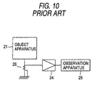
- Fig. 10 is a diagram showing another discharge detection method which is based on the detection of a discharge current.
- reference numeral 21 designates an object apparatus in which a discharge is to be detected
- 26 designates a Rogowski coil
- 24 designates an amplifier
- 25 designates an observation apparatus such as an oscilloscope.
- a pulse current due to a discharge or the like is taken out by the Rogowski coil 26, etc. which is electromagnetically coupled with a grounding conductor for the object apparatus 21.
- the pulse current is amplified by the amplifier 24 and then observed on the oscilloscope 25 or the like.
- the frequency is in a wide band from hundreds kHz to about 1 MHZ.
- the circuit is connected to the apparatus via a conductor and captures a high-frequency signal generated over a wide range in a network of distributed constant circuits which are coupled with each other by spatial capacitances. Consequently, it is very difficult to distinguish an internal discharge to be observed from external noise.
- the S/N ratio is often so poor that the minimum detection level becomes high with the result that such a method cannot be practically used.
- Fig. 11 is a diagram showing a prior art discharge detection method which is based on the detection of a discharge noise and which is disclosed in Institute of Electrical Engineers of Japan, "State and Trend of Preventive Maintenance Technique for Transformer", Technical Report of Institute of Electrical Engineers of Japan (Part II), No. 344, August 1990 (Expert Committee on Preventive Maintenance of Transformer).
- reference numeral 27 designates an interior of an object apparatus which is filled with oil or the like
- 28 designates a tank wall of the object apparatus
- 29 designates a piezoelectric device
- 30 designates a magnet plate
- 31 designates a cable.
- the components 29 to 31 constitute an ultrasonic microphone.
- the ultrasonic microphone is attached to the tank wall 28 of the object apparatus and discharge noise is then detected.
- the sensitivity cannot be increased to a sufficient level.
- it is difficult to remove noise such as a sound produced by collision of rain drops or sand grains with the object apparatus.
- decomposition products are chemically analyzed.
- a fluid insulator oil or gas
- organic insulators that are thermally decomposed by a discharge are dissolved
- An abnormality in the insulation is judged on the basis of the components of the collected gas. The judgment involves a prolonged time period, and requires expert knowledge of thermal decomposition characteristics of insulators and experience.
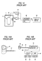
- Figs. 12A and 12B are diagrams showing the corona discharge detector disclosed in Japanese Patent Unexamined Publication No. SHO 62-134574 "CORONA DISCHARGE DETECTOR".
- reference numeral 33 designates a conductor through which a high-voltage current flows and which is fixed to a metal duct 32 via support plates 34
- 35 designates an antenna which detects an electromagnetic wave generated by a corona discharge occurring in the duct and which is fixed to the duct 32. Only when the detection is to be conducted, the antenna 35 is connected to a control unit 37 via a connector 36.
- a corona discharge occurs, an electromagnetic wave is generated by the discharge.
- the antenna is previously disposed at various positions of the duct.
- the portable control unit is connected to the antennas in sequence so that the detection is conducted.
- an electromagnetic wave generated by a corona discharge is detected, it is judged that a corona discharge occurs.
- the antennas are separated from the control unit, and hence the detection cannot be conducted in real time. Consequently, the system has a drawback that a discharge cannot be detected unless an electromagnetic wave is generated when the control unit is connected to one of the antennas.
- the system is effective in the case where insulation deterioration advances to a level where a continued discharge is conducted, but may fail to detect a discharge in the case where insulation deterioration is in an initial stage and a discharge occurs only in a discrete manner.
- Figs. 13 and 14 show prior art examples disclosed in Japanese Patent Unexamined Publication No. HEI 2-297078 "ABNORMALITY DETECTOR FOR AN ELECTRIC APPARATUS" and Japanese Patent Unexamined Publication No. HEI 3-81674 "PARTIAL DISCHARGE DETECTOR FOR AN ELECTRIC APPARATUS".
- reference numeral 38 designates a magnetic sensor in which a wire is wound around a magnetic core plural times in order to detect the magnetic field component of an electromagnetic wave generated by a partial discharge
- 39 designates a sound receiving device which receives an ultrasonic wave generated by a partial discharge
- 40 designates an amplifier-A
- 41 designates an amplifier-B
- 42 designates a discharge detection circuit
- 37 designates a light receiving sensor for ultraviolet rays generated by a partial discharge
- 43 designates a display device.
- an electromagnetic wave and an ultrasonic wave are generated by the partial discharge.
- the electromagnetic wave is detected by the magnetic sensor 38.
- the detected electromagnetic wave is amplified by the amplifier-A 40 and then transmitted to the discharge detection circuit 42.
- the ultrasonic wave is detected by the sound receiving device 39.
- the detected ultrasonic wave is amplified by the amplifier-B 41 and then transmitted to the discharge detection circuit 42.
- the discharge detection circuit receives inputs from both the magnetic sensor and the sound receiving device, the circuit judges that a discharge occurs, and the display device 43 is started to operate.
- the discharge detection circuit receives an input from only one of the magnetic sensor and the sound receiving device, it is judged that there occurs a disturbance.
- the sound receiving device is replaced with the light receiving sensor for detecting ultraviolet rays generated by a partial discharge.
- the method in which an electromagnetic wave generated by a partial discharge is detected by the magnetic sensor is used together with the other method which uses the sound receiving device or the light receiving sensor. Consequently, the system has a drawback that the use of the plural sensors makes the system complicated in structure.
- the magnetic sensor has a structure in which a winding is formed on a magnetic core. Such a structure can detect an electromagnetic wave the frequency of which is several MHZ at the highest. Since electromagnetic waves of this frequency band are already used in many applications with leaving no space between frequencies, it is difficult to prevent a disturbance from entering the magnetic sensor, with the result that the system must be used conjointly with another system.
- Figs. 15A and 15B show a prior art example disclosed in Japanese Patent Unexamined Publication No. HEI 3-239971 "CORONA DISCHARGE DETECTOR".
- reference numeral 45 designates a sensor unit
- 46 designates a group of micro-loop antennas which are different from each other in electromagnetic induction frequency and which cover the frequency range of 10 kHz to 1 GHz as a whole.
- Reference numeral 47 designates a coaxial cable
- 48 designates an apparatus to be measured
- 49 designates a comparison detector
- 50 designates a dummy antenna for noise detection
- 51 designates a CPU
- 52 designates a RAM
- 53 designates a ROM
- 54 designates a CRT
- 55 designates a printer.
- An electromagnetic wave is generated by a corona discharge occurring as a result of insulation deterioration of the apparatus 48 to be measured.
- the components of 10 kHz to 1 GHz of the electromagnetic wave are received by the antenna 46 and then supplied to the comparison detector 49 through the coaxial cable 47.
- Noise of the space is received by the dummy antenna 50 and then supplied to the comparison detector 49.
- the electromagnetic wave generated by the discharge, and the noise are compared with each other, and the comparison output is produced by the comparison detector.
- the comparison output is processed by the CPU 51 and then displayed on the CRT 54 and the printer 55.
- the object frequency in the range of about 1 to 2 GHz.
- An electromagnetic wave generated by a discharge has a wide frequency spectrum as shown in Fig. 16 which extends from a low frequency of several kHz to a microwave of ten-odd GHz, and has a characteristic in which its distribution is substantially proportional to 1/f (where f is a frequency).
- a discharge is to be detected on the basis of an electromagnetic wave, therefore, the detection can be conducted efficiently in a configuration in which an electromagnetic wave of a low frequency is received.
- the low-frequency region useful in the configuration in which an electromagnetic wave of a low frequency is received is in a range where electromagnetic waves are used in an overcrowded manner. Therefore, the configuration has a defect that it is easily affected by another electromagnetic wave, and hence must be used conjointly with a noise/disturbance removing apparatus.
- US-A-5,418,463 teaches a process for detecting arc discharges in power cables connecting power supply board and at least one equipment rack, the power supply board including circuit breakers operable at a certain current level, the arc discharge occurring at a fraction of the current level. After the arc discharge is detected, a signal representing the presence of the arc discharged is supplied to a power supply control, and a control signal is provided by the power supply control to cause the at least one circuit breaker to open interrupting supply of power to an affected power cable.
- an object of the invention is to provide a microwave sensor in which frequency components in the microwave band are extracted and which detects a discharge easily, correctly, and in real time and which is hardly affected by a disturbance.
- a microwave sensor which comprises: an antenna unit which is to be placed in the vicinity of an electric apparatus and which receives a microwave signal generated by a discharge occurring in the electric apparatus; a first band-pass filter which allows a predetermined frequency of the microwave signal received by the antenna unit to pass through the filter; amplifying means for amplifying the microwave signal output from the first band-pass filter; a second band-pass filter which removes noise produced by the amplifying means; converting means for converting the microwave signal output from the second band-pass filter into a video signal; and video amplifying means for amplifying the video signal output from the converting means.
- a microwave sensor which comprises: an antenna unit which is to be placed in the vicinity of an electric apparatus and which receives a microwave signal generated by a discharge occurring in the electric apparatus; a first band-pass filter which allows a predetermined frequency of the microwave signal received by the antenna unit to pass through the filter; amplifying means for amplifying the microwave signal output from the first band-pass filter; signal generating means for outputting an oscillating signal; mixing means for receiving the microwave signal from the amplifying means and the oscillating signal from the signal generating means, and mixing the signals with each other to form an intermediate-frequency signal; a second band-pass filter which removes noise from the intermediate-frequency signal output from the mixing means; intermediate-frequency amplifying means for amplifying the intermediate-frequency signal output from the second band-pass filter; converting means for converting the intermediate-frequency signal output from the intermediate-frequency amplifying means into a video signal; and video amplifying means for amplifying the video signal output from the converting means.
- a microwave sensor which comprises: an antenna unit which is to be placed in the vicinity of an electric apparatus and which receives a microwave signal generated by a discharge occurring in the electric apparatus; a first band-pass filter which allows a predetermined frequency of the microwave signal received by the antenna unit to pass through the filter; amplifying means for amplifying the microwave signal output from the first band-pass filter; signal generating means for outputting an oscillating signal; mixing means for receiving the microwave signal from the amplifying means and the oscillating signal from the signal generating means, and mixing the signals with each other to form an intermediate-frequency signal; a second band-pass filter which removes noise from the intermediate-frequency signal output from the mixing means; intermediate-frequency amplifying means for amplifying the intermediate-frequency signal output from the second band-pass filter; logarithmic amplifying and converting means for amplifying the intermediate-frequency signal output from the second band-pass filter, and converting the signal into a video signal; and video amplifying means for amplifying
- a microwave sensor which comprises: in a stage preceding the amplifying means: coupling means for extracting a part of the microwave signal; comparing means for comparing an electromagnetic wave level of the microwave signal extracted by the coupling means with a predetermined value; attenuating means for attenuating the microwave signal; and switching means for switching the microwave signal to the attenuating means, and, when the electromagnetic wave level of the microwave signal supplied to the comparing means is not lower than the predetermined value, the switching means is automatically switched to the attenuating means.
- a microwave sensor which comprises: in a stage preceding the amplifying means, interrupting means for, when the electromagnetic wave level of the microwave signal is greater than a predetermined value, interrupting the microwave signal, the interrupting means comprising a switch and a terminator.
- a microwave sensor which comprises: in a stage preceding the amplifying means, a limiter which, when the electromagnetic wave level of the microwave signal is greater than a predetermined value, limits the electromagnetic wave level of the microwave signal.
- the microwave sensor of the invention a microwave signal among electromagnetic waves generated by a discharge occurring in an electric apparatus is received, the first band-pass filter allows a predetermined frequency of the microwave signal received by the antenna unit to pass therethrough, and the amplifying means amplifies the microwave signal output from the first band-pass filter.
- the second band-pass filter removes noise produced by the amplifying means, the converting means converts the microwave signal output from the second band-pass filter into a video signal, and the video amplifying means amplifies the video signal output from the converting means.
- the video signal is displayed by arbitrary observation means so that the occurrence of the discharge is detected.
- the mixing means receives the microwave signal and the oscillating signal from the signal generating means, and mixes the signals with each other to form an intermediate-frequency signal, thereby enhancing the stability of the sensor.
- the logarithmic amplifying and converting means amplifies the intermediate-frequency signal, thereby increasing the response range, and converts the signal into a video signal.
- the switching means is automatically switched to the attenuating means so that the microwave signal is attenuated and the dynamic range of the converting means is increased.
- the interrupting means which comprises a switch and a terminator interrupts the microwave signal so as to protect the low noise amplifier from an input of an excessive level.
- the limiter limits the electromagnetic wave level of the microwave signal, thereby protecting the low noise amplifier from an input of an excessive level.
- a first embodiment of the microwave sensor comprises: an antenna unit to be placed in the vicinity of the electric disc apparatus, which receives a microwave signal generated by the discharge; an amplifying means for amplifying a microwave signal output from the first band-pass filter; and a converting means for converting the microwave signal output from the second band-pass filter into a video signal.
- a first band-pass filter is coupled between the output of the antenna unit and the input of the amplifying means. The first band-pass filter allows a predetermined frequency of the microwave signal to pass through the filter.
- a second band-pass filter is coupled between the output of the amplifying means and the input of the converting means. The second band-pass filter removes noise produced by the amplifying means.
- a video amplifying means for amplifying the video signal output is coupled to the output of the converting means.
- the microwave sensor of the present invention comprises: an antenna unit to be placed in the vicinity of the electric apparatus, which receives a microwave signal generated by the discharge; amplifying means for amplifying the microwave signal output from the first band-pass filter and converting means for converting a high frequency signal into a video signal.
- the microwave sensor has a first band-pass filter coupled between the output of the microwave signal received by the antenna unit and the input of the amplifying means, allowing a predetermined frequency of the microwave signal to pass through the filter; signal generating means for outputting an oscillating signal; mixing means for receiving the microwave signal from the amplifying means and the oscillating signal from the signal generating means, and mixing the signals with each other to form an intermediate-frequency signal.
- a second band-pass filter which removes noise from the intermediate-frequency signal output from the mixing means.
- Intermediate-frequency amplifying means amplifies the intermediate-frequency signal output from the second band-pass filter and conveys the amplified intermediate-frequency signal to the converting means.
- the video amplifying means amplifies the video signal output from the converting means and video amplifying means for amplifying the video signal output from the converting means.
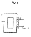
- Fig. 1 is a diagram showing the configuration of the sensor for an electric apparatus according to the invention
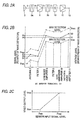
- Fig. 2A is a block diagram of the sensor
- Fig. 2B is a level diagram of a signal and a voltage
- Fig. 2C is a graph showing the input/output characteristics of the sensor for an electric apparatus.
- reference numeral 1 designates a case of an object apparatus in which a discharge may occur
- 2 designates the object apparatus
- 3 designates an antenna which is attached to the object apparatus case 1 and receives a microwave signal generated by a discharge
- 4 designates a signal processing unit which is connected to the antenna 3, amplifies and detects the microwave signal, and amplifies the detected video signal
- 13 designates an output terminal through which the video signal is output.
- the microwave sensor is configured by the antenna 3, the signal processing unit 4, and the output terminal 13.
- Fig. 2A is a block diagram showing the configuration of the sensor for an electric apparatus.
- reference numeral 3 designates the antenna which receives a microwave signal generated by a discharge
- 5a designates a band-pass filter for the high-frequency band which allows a given frequency part of the microwave signal received by the antenna to pass therethrough
- 6 designates a low-noise amplifier which amplifies the output of the band-pass filter 5a
- 5b designates a band-pass filter for the high-frequency band
- 10 designates a wave detector which is converting means for converting the microwave signal output from the band-pass filter 5b into a video signal
- 11 designates a video amplifier which amplifies the video signal
- 13 designates an output terminal through which the video signal is output.
- a microwave signal f1 (for example, 5 GHz as shown in Fig. 16) which is generated by a discharge in the apparatus and has a power of P1 is received by the antenna 3.
- the signal f1 is then output from the antenna with being intensified to a power P2 in accordance with the gain of the antenna.
- the signal f1 passes through the band-pass filter 5a for the high-frequency band, and the output of the filter is reduced to P3 by the loss in the filter.
- the output is amplified by the low-noise amplifier 6 to a level of P4. Only necessary signal components are allowed to pass through the band-pass filter 5b.
- the microwave signal is directly converted by the wave detector 10 into a video signal (of a level of V1) which is a DC signal.
- the video signal is amplified by the video amplifier 11 to a level of V2 and then output through the output terminal 13.
- the band-pass filter 5a allows a frequency of f1 ⁇ hundreds MHZ (for example, f1 ⁇ 100 MHZ) to pass therethrough so that semiconductor devices (such as the low-noise amplifier 6) of the sensor are prevented from being damaged by a low-frequency electromagnetic wave of a high power level.
- Noise is added to the signal f1 by noise involved in the low-noise amplifier 6.
- the band-pass filter 5b is used for removing the noise.
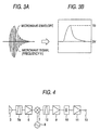
- the output signal is observed by an arbitrary observation apparatus such as an oscilloscope. As shown in Figs. 3A and 3B, for example, the positive or negative half-wave component of an envelope of the microwave signal is displayed on the screen.
- the maximum detection level is indicated by the upper line and the minimum detection level is indicated by the bottom line.
- the electromagnetic power level is varied depending on the manner of discharge.
- the level of an electromagnetic wave which is generated in an initial stage of an abnormality of an electric power apparatus is very low or -100 to -80 dBm. It is required to detect the minimum level.
- the intensity of the discharge is increased, and also the level of the electromagnetic wave generated by the discharge is increased. Consequently, it is preferable to set the dynamic range to be as large as possible.
- the dynamic range is restricted by characteristics (such as saturation) of the parts to be used, whereby the maximum detection level Pmax is determined.
- Fig. 2C shows the input/output characteristics of the sensor.
- a video signal which corresponds to the level of the microwave signal between the minimum and maximum detection levels Pmin and Pmax is output.
- the characteristics depend on those of the semiconductor devices used in the sensor, etc.
- the microwave signal hides behind noises of the sensor itself, resulting in that the microwave signal cannot be detected.
- the level of the microwave signal is not lower than Pmax, amplifiers or the wave detector are saturated so that a video output which is higher in level than Vmax is not obtained.
- the configuration of the embodiment has a receiving sensitivity which is not so high but which is sufficient for a discharge of a high electromagnetic wave level (about -80 to -50 dBm) generated by radiation such as an arc discharge, or a spark discharge. Therefore, the embodiment is suitable for detection of an electromagnetic wave of a relatively high level.
- an electromagnetic wave generated by a discharge has frequency components of a wide band from the low-frequency band to the microwave band.
- the bands lower than the microwave band are occupied by various electromagnetic waves such as broadcast waves and communication waves and hence are easily subjected to interference.
- microwaves are restricted in application, largely attenuated in a space, and hardly affected by an electromagnetic wave in the space. Therefore, microwaves are substantially free from noise.
- the embodiment using a microwave is not required to have a countermeasure against noise which is produced by phenomena other than a discharge, and hence can correctly make judgment.
- a device which removes noise electromagnetic waves is necessary for detection of a discharge.
- such a device is not necessary, and the wave detector directly converts a microwave into a video signal, with the result that the circuit configuration is simple. Since the microwave band is used, furthermore, the portions of the sensor can be configured in a very small size. According to the embodiment, therefore, a microwave sensor which is miniaturized and can be economically produced is provided.
- the directivity of the antenna may be used so that a discharge in an arbitrary space range is detected.
- the portions of the sensor can be configured in a very small size and a non-contact discharge detection method is employed. Consequently, the sensor can be attached without restrictions in insulation distance and manner of attachment.
- a primary phenomenon due to a discharge is electrically captured (discharge - radiation of an electromagnetic wave - detection). Therefore, a discharge is more rapidly detected and more easily judged as compared with a chemical method (discharge - heating - decomposition of organic insulators - collection - analysis - detection).
- the senor can be miniaturized, a number of sensors may be disposed so that the position where an electromagnetic wave is generated is analyzed on the basis of the differences in detection time and level, etc.
- the embodiment is configured so that an electromagnetic wave of a low level is detected without requiring the low-noise amplifier 6 to have a high gain.
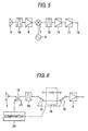
- Fig. 4 is a block diagram showing the configuration of a microwave sensor.
- the components designated by-reference numerals 3, 5a, 6, 10, 11, and 13 are the same as those of Fig. 2A showing Embodiment 1, and their description is omitted.
- Reference numeral 7 designates a mixer which outputs an intermediate-frequency signal corresponding to the difference between the frequency of the microwave signal output from the low-noise amplifier 6 and a given frequency which is oscillated by an oscillator 8.
- Reference numeral 12 designates a band-pass filter for the intermediate-frequency band which removes a spurious generated in the mixer 7, and 9 designates an intermediate-frequency amplifier which amplifies the output of the band-pass filter 12.
- the antenna 3 receives the microwave signal f1 generated by a discharge occurring in an apparatus.
- the signal f1 is passed through the band-pass filter 5a, amplified by the low-noise amplifier 6 to a predetermined level, and then fed to the mixer 7.
- a signal of a frequency of f2 is supplied from the output of the oscillator 8 to the mixer 7.
- the frequency f2 is previously determined so that the signal f3 has an intermediate frequency of about hundreds MHZ.
- a necessary signal is taken out from the signal by the band-pass filter 12, amplified by the intermediate-frequency amplifier 9, and then converted into a video signal by the wave detector 10.
- the video signal is amplified by the video amplifier 11 and then output through the output terminal 13.
- the mixer 7 conducts the frequency conversion, spuriouses of 2f1- f2 and 2f2 - f1 are generated.
- the band-pass filter 12 is used for removing the spuriouses.
- the output signal delivered from the output terminal is observed by an arbitrary observation apparatus such as an oscilloscope.
- a low-noise amplifier When amplification is to be conducted at a single frequency, a low-noise amplifier must have a high gain. In an amplifier for a single frequency and of a high gain, however, there often arise problems such as oscillation. In the configuration described above, the frequency is converted and the amplifiers are separately provided for the high-frequency and intermediate-frequency portions, respectively. Therefore, the stability of the sensor is increased and problems such as oscillation are prevented from arising.
- the gain of an amplifier can be made higher in a stable manner as the frequency is lower. Consequently, the gain of the intermediate-frequency amplifier 9 can be easily set to be higher and that of the low-noise amplifier 6 to be lower, so that an electromagnetic wave which is generated by a discharge and has a low level is surely detected, thereby improving the detection performance.
- Fig. 5 is a block diagram showing the configuration of a microwave sensor.
- the components designated by reference numerals 3, 5a, 6, 7, 8, 12, 11, and 13 are the same as those of Fig. 4 showing Embodiment 2, and their description is omitted.
- Reference numeral 14 designates a logarithmic amplifier which conducts linear-logarithmic conversion and amplification on the output of the band-pass filter 12 and then outputs it in the form of a video signal.
- the antenna 3 receives the microwave signal f1 generated by a discharge occurring in an apparatus.
- the signal f1 is passed through the band-pass filter 5a, amplified by the low-noise amplifier 6 to a predetermined level, and then fed to the mixer 7.
- a signal of a frequency of f2 is supplied from the output of the oscillator 8 to the mixer 7.
- the signal f3 output from the mixer 7 passes through the band-pass filter 12 for the intermediate-frequency band so that only a necessary signal is extracted.
- the extracted signal is subjected to linear-logarithmic conversion and amplification in the logarithmic amplifier 14, and then output in the form of a video signal.
- the video signal is amplified by the video amplifier 11 and then output.
- the embodiment in contrast to the response range of about 20 to 30 dB in Embodiment 2, the embodiment can ensure the response range of 50 to 60 dB, with the result that an increase of at least 20 dB is attained. Therefore, a 100-fold response range can be obtained at the minimum.
- the response range can be expanded and the detection performance can be further improved.
- Fig. 6 is a block diagram of portions of a microwave sensor ranging from the antenna 3 to the low-noise amplifier 6.
- the components designated by reference numerals 3, 5a, and 6 are the same as those of Fig. 2 showing Embodiment 1, and their description is omitted.
- Reference numeral 15 designates a switch for switching an attenuator group 16
- 19 designates a coupler which extracts a part of the microwave signal
- 20 designates a comparator which conducts a comparison on the microwave signal extracted by the coupler 19 and supplies a signal to the switch 15.
- the portions following the low-noise amplifier are the same as those of Embodiments 1 and 2.
- the antenna 3 receives the microwave signal f1 generated by a discharge occurring in an apparatus.
- the signal f1 passes through the band-pass filter 5a, and also the attenuator group 16 to which the switch 15 is switched so that the level of the signal is attenuated. Thereafter, the signal is fed to the low-noise amplifier 6.
- the dynamic range of the wave detector 10 is limited to about 30 dB.
- the dynamic range of the sensor can be increased to a larger value, for example, 60 dB in the case where the value of the attenuator is 30 dB.
- the operations following the low-noise amplifier are the same as those of Embodiments 1 and 2.
- the switch 15 is automatically switched by a control signal.
- the control signal is output from the comparator 20 which compares the level of the part of the microwave signal f1 extracted by the coupler 19 with a given level.
- the dynamic range of the sensor can be increased and the detection performance can be further improved.
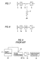
- Fig. 7 is a block diagram of portions of a microwave sensor ranging from the antenna 3 to the low-noise amplifier 6.
- the components designated by reference numerals 3, 5a, 15, and 6 are the same as those of Figs. 2 and 6, and their description is omitted.
- Reference numeral 17 designates a terminator to which the microwave signal is allowed to be input by the switching operation of the switch 15.
- the antenna 3 receives the microwave signal f1 generated by a discharge occurring in an apparatus.
- the signal f1 is passed through the band-pass filter 5a and then fed to the low-noise amplifier 6 via the switch 15.
- the operations following the low-noise amplifier are the same as those of Embodiments 1 to 3.
- the switch 15 is normally connected to the low-noise amplifier 6.
- the state of the switch 15 is changed so that the switch is connected to the terminator 17. This prevents the low-noise amplifier 6 from an input of an excessive level, thereby enhancing the reliability of the sensor.
- a detector which comprises the coupler 19 and the comparator 20 may be connected in a stage preceding the switch 15 so that, when a signal of an excessive level which may destroy the low-noise amplifier 6 is input, the switch 15 is automatically switched to the terminator 17.
- the low-noise amplifier can be protected from an input of an excessive level, thereby enhancing the reliability of the sensor.
- Fig. 8 is a block diagram of portions of a microwave sensor ranging from the antenna to the low-noise amplifier.
- the components designated by reference numerals 3, 5a, and 6 are the same as those of Fig. 2, and their description is omitted.
- Reference numeral 18 designates a limiter which prevents a microwave signal of an excessive level from entering.
- the antenna 3 receives the microwave signal f1 generated by a discharge occurring in an apparatus.
- the signal f1 is passed through the band-pass filter 5a and then fed to the low-noise amplifier 6 via the limiter 18 for protection against an input of an excessive level.
- the operations following the low-noise amplifier are the same as those of Embodiments 1 to 3.
- the level of an electromagnetic wave entering the sensor is very low.
- the limiter 18 is inserted into the stage preceding the low-noise amplifier 6 so that a signal which is higher than a certain level does not enter the amplifier. This prevents the low-noise amplifier 6 from an input of an excessive level so that the reliability of the sensor is enhanced.
- the low-noise amplifier can be protected from an input of an excessive level, thereby enhancing the reliability of the sensor.
- Fig. 17 is a diagram showing the operation of a microwave sensor which is directed toward a closed space configured by a metal.
- reference numerals 3, 4, and 13 designate an antenna of the microwave sensor of the invention, a signal processing unit, and a video output, respectively
- 56 designates a closed space such as a case which is hermetically closed by a metal
- 57 designates a discharge source
- 58 and 59 designate propagation paths for an electromagnetic wave.
- the microwave sensor comprises: an antenna unit which receives a microwave signal generated by a discharge occurring in an electric apparatus; a first band-pass filter which allows a predetermined frequency of the microwave signal received by the antenna unit to pass therethrough; amplifying means for amplifying the microwave signal output from the first band-pass filter; a second band-pass filter which removes noise produced by the amplifying means; converting means for converting the microwave signal output from the second band-pass filter into a video signal; and video amplifying means for amplifying the video signal output from the converting means. Therefore, the microwave sensor is not affected by a disturbance, has high reliability, and can surely detect a discharge. Since the microwave band is used, furthermore, the body of the sensor can be miniaturized. This allows a number of sensors to be attached to an apparatus so that the position is determined.
- the microwave sensor according to the second embodiment comprises signal generating means for outputting an oscillating signal, and mixing means for receiving the microwave signal from the amplifying means and the oscillating signal from the signal generating means, and mixing the signals with each other to form an intermediate-frequency signal. Therefore, the stability of the sensor is increased and a discharge of a low level can be surely detected.
- the microwave sensor may comprise logarithmic amplifying means for amplifying the intermediate-frequency signal, and converting the signal into a video signal. Therefore, the response range can be increased and the detection performance can be further improved.
- the switching means is automatically switched to the attenuating means. Therefore, the dynamic range of the sensor can be increased and the detection performance can be further improved.
- the microwave sensor may comprise interrupting means for, when the electromagnetic wave level of the microwave signal is greater than a predetermined value, interrupting the microwave signal.
- the interrupting means comprises a switch and a terminator. Therefore, the low-noise amplifier can be protected from an input of an excessive level, thereby enhancing the reliability of the sensor.
- the microwave sensor may comprise a limiter which, when the electromagnetic wave level of the microwave signal is greater than a predetermined value, limits the electromagnetic wave level of the microwave signal which is fed to low-noise amplifier. Therefore, the low-noise amplifier can be protected from an input of an excessive level, thereby enhancing the reliability of the sensor.
Landscapes
- Physics & Mathematics (AREA)
- General Physics & Mathematics (AREA)
- Electromagnetism (AREA)
- Testing Relating To Insulation (AREA)
Claims (6)
- Mikrowellensensor, geeignet zur Erkennung einer Entladung, die in einem elektrischen Gerät stattfindet, folgendes aufweisend:wobei der Mikrowellensensor dadurch gekennzeichnet ist, dasseine Antenneneinheit (3), die in der Nähe des elektrischen Geräts angeordnet wird, die ein Mikrowellensignal empfängt, das durch die Entladung erzeugt wird;eine Verstärkereinrichtung (6), um das Mikrowellensignal zu verstärken;eine Wandlereinrichtung (10), um ein verstärktes Mikrowellensignal in ein Videosignal umzuwandeln;
ein erstes Bandpassfilter (5a) zwischen dem Ausgang der Antenneneinheit (3) und dem Eingang der Verstärkermittel (6) gekoppelt ist, wobei das erste Bandpassfilter einer vorbestimmten Frequenz des Mikrowellensignals erlaubt, das Filter zu durchlaufen;
ein zweites Bandpassfilter (5b) zwischen dem Ausgang der Verstärkereinrichtung (6) und dem Eingang der Wandlereinrichtung (10) gekoppelt ist, wobei das zweite Bandpassfilter Rauschen beseitigt, das durch die Verstärkereinrichtung (6) erzeugtes wird; und
eine Videoverstärkereinrichtung (11) zum Verstärken des Videoausgangssignals an den Ausgang der Wandlereinrichtung (10) gekoppelt ist. - Mikrowellensensor, geeignet zur Erkennung einer Entladung, die in einem elektrischen Gerät stattfindet, folgendes aufweisend:wobei der Mikrowellensensor gekennzeichnet ist durcheine Antenneneinheit (3), die in der Nähe des elektrischen Geräts angeordnet wird, die ein Mikrowellensignal empfängt, das durch die Entladung erzeugt wird;eine Verstärkereinrichtung (6), um das Mikrowellensignal zu verstärken;eine Wandlereinrichtung (10, 14), um ein Hochfrequenzsignal in ein Videosignal umzuwandeln;
ein erstes Bandpassfilter (5a), das zwischen dem Ausgang des Mikrowellensignals, das durch die Antenneneinheit (3) empfangen wird, und dem Eingang der Verstärkereinrichtung (6) gekoppelt ist, wobei es einer vorbestimmten Frequenz des Mikrowellensignals erlaubt, das Filter zu durchlaufen;
eine Signalerzeugungseinrichtung (8), um ein Schwingungssignal auszugeben;
eine Mischeinrichtung (7), um das Mikrowellensignal von der Verstärkereinrichtung (6) und das Schwingungssignal von der Signalerzeugungseinrichtung (8) zu empfangen und die Signale miteinander zu vermischen, um ein Zwischenfrequenzsignal zu bilden;
ein zweites Bandpassfilter (12), welches Rauschen von dem Zwischenfrequenzsignal beseitigt, das von der Mischeinrichtung (7) ausgegeben wird;
eine Zwischenfrequenzverstärkereinrichtung (9), um das Zwischenfrequenzsignal zu verstärken, das von dem zweiten Bandpassfilter (12) ausgegeben wird, und um das verstärkte Zwischenfrequenzsignal an die Wandlereinrichtung (10, 14) zu übermitteln; und
eine Videoverstärkereinrichtung (11), um das Videosignal zu verstärken, das von der Wandlereinrichtung (10, 14) ausgegeben wird. - Mikrowellensensor nach Anspruch 1,
wobei die Wandlereinrichtung eine logarithmische Verstärker- und Wandlereinrichtung (14) aufweist, um das Zwischenfrequenzsignal zu verstärken, das von dem zweiten Bandpassfilter (12) ausgegeben wird und um das Signal in ein Videosignal umzuwandeln. - Mikrowellensensor nach Anspruch 1 oder 2,
ferner in einer Stufe, die der Verstärkereinrichtung (6) vorangeht; folgendes aufweisend:eine Kopplungseinrichtung (19), um einen Teil des Mikrowellensignals zu extrahieren; eine Vergleichseinrichtung (20), um einen elektromagnetischen Wellenpegel des Mikrowellensignals, das durch die Kopplungseinrichtung extrahiert wird, mit einem vorbestimmten Wert zu vergleichen;eine Dämpfungseinrichtung (16), um das Mikrowellensignal zu dämpfen; undeine Schalteinrichtung (15), um das Mikrowellensignal an die Dämpfungseinrichtung (16) umzuschalten und um die Schalteinrichtung (15) automatisch an die Dämpfungseinrichtung (16) umzuschalten, wenn der elektromagnetische Wellenpegel des Mikrowellensignals, das der Vergleichseinrichtung (20) bereitgestellt wird, nicht geringer als der vorbestimmte Wert ist. - Mikrowellensensor nach Anspruch 1 oder 2,
ferner in einer Stufe, die der Verstärkereinrichtung (6) vorangeht, folgendes aufweisend:eine Unterbrechungseinrichtung, um, wenn der elektromagnetische Wellenpegel des Mikrowellensignals größer als ein vorbestimmter Wert ist, das Mikrowellensignal zu unterbrechen, wobei die Unterbrechungseinrichtung einen Schalter (15) und einen Terminator (17) aufweist. - Mikrowellensensor nach Anspruch 1 oder 2,
ferner in einer Stufe, die der Verstärkereinrichtung (6) vorangeht, folgendes aufweisend:einen Begrenzer bzw. Limiter (18), der, wenn der elektromagnetische Wellenpegel des Mikrowellensignals größer als ein vorbestimmter Wert ist, den elektromagnetischen Wellenpegel des Mikrowellensignals begrenzt.
Priority Applications (3)
| Application Number | Priority Date | Filing Date | Title |
|---|---|---|---|
| US08/630,817 US5726576A (en) | 1996-04-10 | 1996-04-10 | Microwave sensor for detecting a discharge occurring in an electrical apparatus |
| EP96105891A EP0802421B1 (de) | 1996-04-10 | 1996-04-15 | Mikrowellensensor |
| DE69626786T DE69626786T2 (de) | 1996-04-15 | 1996-04-15 | Mikrowellensensor |
Applications Claiming Priority (2)
| Application Number | Priority Date | Filing Date | Title |
|---|---|---|---|
| US08/630,817 US5726576A (en) | 1996-04-10 | 1996-04-10 | Microwave sensor for detecting a discharge occurring in an electrical apparatus |
| EP96105891A EP0802421B1 (de) | 1996-04-10 | 1996-04-15 | Mikrowellensensor |
Publications (2)
| Publication Number | Publication Date |
|---|---|
| EP0802421A1 EP0802421A1 (de) | 1997-10-22 |
| EP0802421B1 true EP0802421B1 (de) | 2003-03-19 |
Family
ID=26141867
Family Applications (1)
| Application Number | Title | Priority Date | Filing Date |
|---|---|---|---|
| EP96105891A Expired - Lifetime EP0802421B1 (de) | 1996-04-10 | 1996-04-15 | Mikrowellensensor |
Country Status (2)
| Country | Link |
|---|---|
| US (1) | US5726576A (de) |
| EP (1) | EP0802421B1 (de) |
Families Citing this family (13)
| Publication number | Priority date | Publication date | Assignee | Title |
|---|---|---|---|---|
| WO1997042512A1 (en) * | 1996-05-08 | 1997-11-13 | Mitsubishi Denki Kabushiki Kaisha | Abnormality detection apparatus and abnormality detection method |
| SE9700836L (sv) * | 1997-03-10 | 1998-09-07 | Abb Research Ltd | Anordning för avkänning av elektriska urladdningar i ett provobjekt med två elektriska anslutningsledare |
| US6242922B1 (en) * | 1998-11-06 | 2001-06-05 | General Electric Company | Arc detection architecture based on correlation for circuit breakers |
| US6300767B1 (en) * | 1998-11-30 | 2001-10-09 | General Electric Company | System and apparatus for predicting failure in insulated systems |
| US6172862B1 (en) | 1999-06-11 | 2001-01-09 | Anthony J. Jonnatti | Partial discharge relay and monitoring device |
| JP3628244B2 (ja) | 2000-08-28 | 2005-03-09 | 株式会社日立製作所 | 部分放電検出方法 |
| RU2207581C2 (ru) * | 2001-04-17 | 2003-06-27 | Марийский государственный университет | Способ определения состояния линейной изоляции распределительных сетей и определения места её повреждения |
| US7183776B1 (en) * | 2005-08-31 | 2007-02-27 | Electrical Reliability Services, Inc. | System and method for performing online partial discharge testing |
| RU2365928C1 (ru) * | 2007-12-03 | 2009-08-27 | Государственное образовательное учреждение высшего профессионального образования Иркутский государственный университет путей сообщения (ИрГУПС(ИрИИТ)) | Способ дистанционной акустоэлектромагнитной диагностики состояния линейной изоляции контактной сети переменного тока железнодорожного транспорта |
| US20090267846A1 (en) * | 2008-04-28 | 2009-10-29 | Johnson Michael P | Electromagnetic Field Power Density Monitoring System and Methods |
| US8115475B2 (en) | 2009-09-23 | 2012-02-14 | Electrical Reliability Services, Inc. | Manipulation assembly for online electrical system test probe installation |
| KR101095778B1 (ko) * | 2009-12-28 | 2011-12-21 | 주식회사 효성 | 전력 변압기를 위한 부분방전 검출장치 |
| JP7362205B2 (ja) * | 2019-08-26 | 2023-10-17 | 日東工業株式会社 | 放電検出装置 |
Family Cites Families (13)
| Publication number | Priority date | Publication date | Assignee | Title |
|---|---|---|---|---|
| US4006410A (en) * | 1975-12-19 | 1977-02-01 | Lee A. Chagra | Corona discharge detection system for detecting the presence of any corona discharge in an electrical system |
| US4346716A (en) * | 1980-03-31 | 1982-08-31 | M/A Com, Inc. | Microwave detection system |
| JPS62134574A (ja) * | 1985-12-06 | 1987-06-17 | Mitsubishi Electric Corp | コロナ放電検知装置 |
| JPH02297078A (ja) * | 1989-05-11 | 1990-12-07 | Toshiba Corp | 電気機器の異常検出装置 |
| JPH0381674A (ja) * | 1989-08-25 | 1991-04-08 | Toshiba Corp | 電気機器の部分放電検出装置 |
| JPH07109428B2 (ja) * | 1990-02-16 | 1995-11-22 | 東京電力株式会社 | コロナ放電検出器 |
| GB9021484D0 (en) * | 1990-10-03 | 1990-11-14 | Univ Strathclyde | Gas insulated substations |
| KR100212020B1 (ko) * | 1990-10-24 | 1999-08-02 | 제임스 제이. 키넌 | 전기아크 및 고주파 스펙트럼 검출 |
| US5270509A (en) * | 1991-12-24 | 1993-12-14 | Electric Power Research Institute | Microwave clothes drying system and method with improved arc detection |
| US5499189A (en) * | 1992-09-21 | 1996-03-12 | Radar Engineers | Signal processing method and apparatus for discriminating between periodic and random noise pulses |
| US5418463A (en) * | 1993-11-24 | 1995-05-23 | At&T Corp. | Detection of arcs in power cables using plasma noise or negtive resistance of the arcs |
| DE4420448C1 (de) * | 1994-06-10 | 1995-09-14 | Fraunhofer Ges Forschung | Verfahren und Vorrichtung zur Messung der Feldstärke in einem Funkkanal und dessen Nachbarkanälen mittels Zero-IF |
| US5608328A (en) * | 1994-11-18 | 1997-03-04 | Radar Engineers | Method and apparatus for pin-pointing faults in electric power lines |
-
1996
- 1996-04-10 US US08/630,817 patent/US5726576A/en not_active Expired - Fee Related
- 1996-04-15 EP EP96105891A patent/EP0802421B1/de not_active Expired - Lifetime
Also Published As
| Publication number | Publication date |
|---|---|
| EP0802421A1 (de) | 1997-10-22 |
| US5726576A (en) | 1998-03-10 |
Similar Documents
| Publication | Publication Date | Title |
|---|---|---|
| US7746082B2 (en) | Partial discharge detection device | |
| US5726576A (en) | Microwave sensor for detecting a discharge occurring in an electrical apparatus | |
| JP3251593B2 (ja) | 異常検知装置及び異常検知方法 | |
| US5903159A (en) | Microwave sensor for sensing discharge faults | |
| US11843236B2 (en) | Arc detection system and method for an aircraft high voltage and direct current electrical circuit | |
| KR101753642B1 (ko) | 수배전반의 부분방전 검출방법 | |
| JP2008304357A (ja) | 部分放電計測装置 | |
| KR101771554B1 (ko) | 부분방전 검출장치를 구비한 수배전반 | |
| US5418463A (en) | Detection of arcs in power cables using plasma noise or negtive resistance of the arcs | |
| CN1162746A (zh) | 微波探测器 | |
| JPH08129047A (ja) | マイクロ波センサー | |
| JP4342993B2 (ja) | 金属閉鎖型配電盤の絶縁監視装置 | |
| JPH03293908A (ja) | 絶縁監視用アンテナ装置 | |
| JP3176000B2 (ja) | スイッチギヤの部分放電検出装置 | |
| JP3682930B2 (ja) | 絶縁劣化診断装置 | |
| JP2598404Y2 (ja) | ガス絶縁開閉装置用異常監視装置 | |
| JPH0817298A (ja) | 電気開閉装置用の放電検出装置 | |
| JP2723902B2 (ja) | スペクトラム減算方式部分放電監視システム | |
| KR102387732B1 (ko) | 내부의 열화감시를 위한 마이크로 스트립 안테나가 장착된 함체 | |
| JPH0524466B2 (de) | ||
| DE69626786T2 (de) | Mikrowellensensor | |
| JPH0522874B2 (de) | ||
| JP2950425B2 (ja) | 電気機器の部分放電監視装置 | |
| JPH10322823A (ja) | 電気機器の絶縁診断方法及び装置 | |
| JPS63145974A (ja) | 電気機器の部分放電検出方法 |
Legal Events
| Date | Code | Title | Description |
|---|---|---|---|
| PUAI | Public reference made under article 153(3) epc to a published international application that has entered the european phase |
Free format text: ORIGINAL CODE: 0009012 |
|
| 17P | Request for examination filed |
Effective date: 19970204 |
|
| AK | Designated contracting states |
Kind code of ref document: A1 Designated state(s): DE GB SE |
|
| 17Q | First examination report despatched |
Effective date: 20010116 |
|
| GRAH | Despatch of communication of intention to grant a patent |
Free format text: ORIGINAL CODE: EPIDOS IGRA |
|
| GRAH | Despatch of communication of intention to grant a patent |
Free format text: ORIGINAL CODE: EPIDOS IGRA |
|
| GRAA | (expected) grant |
Free format text: ORIGINAL CODE: 0009210 |
|
| AK | Designated contracting states |
Designated state(s): DE GB SE |
|
| REG | Reference to a national code |
Ref country code: GB Ref legal event code: FG4D |
|
| REF | Corresponds to: |
Ref document number: 69626786 Country of ref document: DE Date of ref document: 20030424 Kind code of ref document: P |
|
| REG | Reference to a national code |
Ref country code: SE Ref legal event code: TRGR |
|
| PLBE | No opposition filed within time limit |
Free format text: ORIGINAL CODE: 0009261 |
|
| STAA | Information on the status of an ep patent application or granted ep patent |
Free format text: STATUS: NO OPPOSITION FILED WITHIN TIME LIMIT |
|
| 26N | No opposition filed |
Effective date: 20031222 |
|
| PGFP | Annual fee paid to national office [announced via postgrant information from national office to epo] |
Ref country code: SE Payment date: 20050406 Year of fee payment: 10 |
|
| PGFP | Annual fee paid to national office [announced via postgrant information from national office to epo] |
Ref country code: DE Payment date: 20050407 Year of fee payment: 10 |
|
| PGFP | Annual fee paid to national office [announced via postgrant information from national office to epo] |
Ref country code: GB Payment date: 20050413 Year of fee payment: 10 |
|
| PG25 | Lapsed in a contracting state [announced via postgrant information from national office to epo] |
Ref country code: GB Free format text: LAPSE BECAUSE OF NON-PAYMENT OF DUE FEES Effective date: 20060415 |
|
| PG25 | Lapsed in a contracting state [announced via postgrant information from national office to epo] |
Ref country code: SE Free format text: LAPSE BECAUSE OF NON-PAYMENT OF DUE FEES Effective date: 20060416 |
|
| PG25 | Lapsed in a contracting state [announced via postgrant information from national office to epo] |
Ref country code: DE Free format text: LAPSE BECAUSE OF NON-PAYMENT OF DUE FEES Effective date: 20061101 |
|
| EUG | Se: european patent has lapsed | ||
| GBPC | Gb: european patent ceased through non-payment of renewal fee |
Effective date: 20060415 |