EP0802556B1 - Wechselstrom-Plasma-Anzeigetafel - Google Patents
Wechselstrom-Plasma-Anzeigetafel Download PDFInfo
- Publication number
- EP0802556B1 EP0802556B1 EP97105986A EP97105986A EP0802556B1 EP 0802556 B1 EP0802556 B1 EP 0802556B1 EP 97105986 A EP97105986 A EP 97105986A EP 97105986 A EP97105986 A EP 97105986A EP 0802556 B1 EP0802556 B1 EP 0802556B1
- Authority
- EP
- European Patent Office
- Prior art keywords
- electrodes
- maintaining
- electrode
- scanning
- discharge
- Prior art date
- Legal status (The legal status is an assumption and is not a legal conclusion. Google has not performed a legal analysis and makes no representation as to the accuracy of the status listed.)
- Expired - Lifetime
Links
Images


Classifications
-
- H—ELECTRICITY
- H01—ELECTRIC ELEMENTS
- H01J—ELECTRIC DISCHARGE TUBES OR DISCHARGE LAMPS
- H01J11/00—Gas-filled discharge tubes with alternating current induction of the discharge, e.g. alternating current plasma display panels [AC-PDP]; Gas-filled discharge tubes without any main electrode inside the vessel; Gas-filled discharge tubes with at least one main electrode outside the vessel
- H01J11/20—Constructional details
- H01J11/22—Electrodes, e.g. special shape, material or configuration
-
- H—ELECTRICITY
- H01—ELECTRIC ELEMENTS
- H01J—ELECTRIC DISCHARGE TUBES OR DISCHARGE LAMPS
- H01J11/00—Gas-filled discharge tubes with alternating current induction of the discharge, e.g. alternating current plasma display panels [AC-PDP]; Gas-filled discharge tubes without any main electrode inside the vessel; Gas-filled discharge tubes with at least one main electrode outside the vessel
- H01J11/10—AC-PDPs with at least one main electrode being out of contact with the plasma
- H01J11/12—AC-PDPs with at least one main electrode being out of contact with the plasma with main electrodes provided on both sides of the discharge space
-
- H—ELECTRICITY
- H01—ELECTRIC ELEMENTS
- H01J—ELECTRIC DISCHARGE TUBES OR DISCHARGE LAMPS
- H01J11/00—Gas-filled discharge tubes with alternating current induction of the discharge, e.g. alternating current plasma display panels [AC-PDP]; Gas-filled discharge tubes without any main electrode inside the vessel; Gas-filled discharge tubes with at least one main electrode outside the vessel
- H01J11/20—Constructional details
- H01J11/22—Electrodes, e.g. special shape, material or configuration
- H01J11/32—Disposition of the electrodes
-
- H—ELECTRICITY
- H01—ELECTRIC ELEMENTS
- H01J—ELECTRIC DISCHARGE TUBES OR DISCHARGE LAMPS
- H01J2211/00—Plasma display panels with alternate current induction of the discharge, e.g. AC-PDPs
- H01J2211/20—Constructional details
- H01J2211/22—Electrodes
- H01J2211/32—Disposition of the electrodes
- H01J2211/323—Mutual disposition of electrodes
-
- H—ELECTRICITY
- H01—ELECTRIC ELEMENTS
- H01J—ELECTRIC DISCHARGE TUBES OR DISCHARGE LAMPS
- H01J2211/00—Plasma display panels with alternate current induction of the discharge, e.g. AC-PDPs
- H01J2211/20—Constructional details
- H01J2211/22—Electrodes
- H01J2211/32—Disposition of the electrodes
- H01J2211/326—Disposition of electrodes with respect to cell parameters, e.g. electrodes within the ribs
Definitions
- the present invention relates to an AC plasma display panel by which an image display of television or an advertising display board is obtained.
- EP-A-0 680 067 describes an AC plasma display panel comprising first and second glass substrates that face each other and define a discharge space between them.
- a plurality of scanning electrodes and sustaining electrodes being parallel to each other are formed on the first glass substrate.
- a dielectric layer covers said scanning electrodes and said sustaining electrodes and a plurality of barriers and data electrodes are formed on the second glass substrate and are arranged parallel to said scanning electrodes and said sustaining electrodes.
- a discharge cell which is formed by a pair of adjacent barriers comprises a plurality of scanning electrodes and a plurality of sustaining electrodes.
- the substrates may be formed of ceramic provided that at least on of the substrates is transparent to allow the transmission of a discharge light.
- a discharge cell 2 comprises a pair of electrodes consisting of a scanning electrode 3 and a maintaining electrode 4 that are parallel to each other and formed on a first glass substrate 1.
- the scanning electrode 3 and the maintaining electrode 4 are covered with a dielectric layer 5 and a protective film layer 6.
- a second glass substrate 7 which is facing the first glass substrate 1
- a plurality of ribs 9 are arranged orthogonally to the scanning electrode 3 and the maintaining electrode 4.
- a data electrode 8 is arranged parallel to and between two ribs 9.
- On the surface of the second glass substrate 7 and the data electrode 8 positioned between the ribs 9, a phosphor layer 10 is provided.
- a discharge space 11 which is surrounded by the glass substrate 1, the second substrate 7 and ribs 9, is formed.
- a discharge cell 2 which is a region where a pair of electrodes consisting of a scanning electrode 3 and a maintaining electrode 4 and two ribs 9 are crossing each other, is formed.
- a scanning electrode 3, a maintaining electrode 4 and the data electrode 8 are composed of Ag or a laminated conductor in which a Cu layer is sandwiched by Cr layers.
- the dielectric layer 5 is composed of borosilicate glass and the like, and the protective film layer 6 is composed of MgO and the like.
- at least one discharge noble gas such as helium, neon, argon, xenon and the like is sealed.
- FIG. 11 is a sectional view of a discharge cell taken on line XI-XI of FIG. 10.
- a positive write pulse voltage is applied to a data electrode 8 and a negative scanning pulse voltage is applied to a scanning electrode 3. Consequently, a write discharge is generated in the discharge space 11, and therefore a positive electrical charge is stored on a surface of a protective film layer 6 formed on the scanning electrode 3.
- a negative pulse voltage is applied to a maintaining electrode 4, and consequently a maintaining discharge is excited by the positive electrical discharge generated on the surface of the protective film layer 6 formed on the scanning electrode 3.
- the maintaining charge is continued by applying a negative pulse voltage to the scanning electrode 3 and the maintaining electrode 4 alternately.
- the maintaining discharge is ceased by applying a negative erasing pulse voltage to the maintaining electrode 4.
- the maintaining discharge is generated at a limited region S with a comparatively strong electric field.
- Ultraviolet rays emitted from the region S excite a phosphor layer 10, than a visible light emitted from the phosphor layer 10 passes externally through the first glass substrate 1 as shown by dotted lines in FIG. 11.
- the distance W between the scanning electrode 3 and the maintaining electrode 4 is widened, the maintaining discharge region S is widened, and as a result, the amount of ultraviolet rays is increased.
- the luminous efficiency of the maintaining discharge can be improved, however, the maintaining discharge voltage is also increased considerably with the great increase of the amount of the ultraviolet rays. Therefore the distance W between the scanning electrode 3 and the maintaining electrode 4 is set in a range between 20 ⁇ m and 200 ⁇ m, taking into consideration the requirements for practical use.
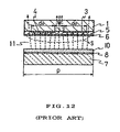
- FIG. 12 is a sectional view in which the width of each electrode d 0 as shown in FIG. 11 is widened.
- a maintaining discharge region S in a discharge cell 2 is widened, as a result, a large amount of ultraviolet rays is obtained. Consequently, the amount of visible light emitting from the phosphor layer 10 is increased.
- the width of electrode d 0 is widened, the area where visible light emitting from a phorphor layer 10 is interrupted by the scanning electrode 3 and the maintaining electrode 4 is increased. Consequently, the opening ratio which is the ratio of an area where a visible light passes to an area of discharge cell, is reduced. Therefore, when the width of electrode d 0 exceeds a certain amount, the brightness is reduced conversely.
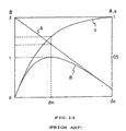
- FIG. 13 is a graph showing the relationship between the width of scanning electrode 3 and maintaining electrode 4, shown as d 0 , the amount of ultraviolet rays shown as u, opening ratio of panel shown as A and the brightness of the panel shown as B.
- the scale used in FIG. 13 is a relative scale, and the maximum value of B, A and u respectively is 1.
- the width of the electrode do exceeds a certain amount the brightness B is reduced by an influence of the reduction of the opening ratio A.
- FIG. 13 is a graph showing the relationship between the width of scanning electrode 3 and maintaining electrode 4, shown as d 0 , the amount of ultraviolet rays shown as u, opening ratio of panel shown as A and the brightness of the panel shown as B.
- the scale used in FIG. 13 is a relative scale, and the maximum value of B, A and
- the width of an electrode d 0 when the width of an electrode d 0 is dm, the brightness B becomes maximum. Therefore the width of the scanning electrode 3 and the maintaining electrode 4 d 0 are set to be dm.
- W is in a range between 20 ⁇ m and 200 ⁇ m and the width of a discharge cell is shown as p
- dm satisfies two conditions, such as dm+W is in a range between 200 ⁇ m and 2000 ⁇ m, and dm is in a range between p/5 and p/3.
- a scanning electrode 3 and a scanning electrode bus 3a are connected electrically.
- a maintaining electrode 4 and a maintaining electrode bus 4a are also connected electrically.
- the scanning electrode 3 and the maintaining electrode 4 are composed of a transparent conductor such as ITO or SnO 2 .
- the scanning electrode bus 3a, the maintaining electrode bus 4a and a data electrode 8 are composed of Ag or a laminated conductor in which a Cu layer is sandwiched by Cr layers.
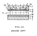
- FIG. 15 is a sectional view of a discharge cell 2 taken on line XV-XV of FIG. 14.
- the scanning electrode 3 and the maintaining electrode 4 are composed of a transparent conductor. Therefore, as shown by dotted lines in FIG. 15, a visible light emitting from the phosphor layer 10 passes through those electrodes easily. Consequently, even if the width of the scanning electrode 3 and the maintaining electrode 4 d 1 is widened, the area, where a visible light passes through, is not changed, and as a result, the opening ratio is maintained to be constant. Therefore, the maintaining discharge region S can be widened without decreasing the opening ratio. As a result, a decrease of brightness due to a decrease of the opening ratio can be prevented and the luminous efficiency of the maintaining discharge can be improved.
- the maintaining discharge region S can be widened and the amount of ultraviolet rays can be increased by widening a width of an electrode d 0 .
- the width of an electrode exceeds a certain amount, the brightness is decreased conversely by the effect of the decrease of the opening ratio. Consequently, there is a certain limitation to achieve a high brightness and high efficiency.
- the above-mentioned problems of the first example are solved.
- it is required to form a scanning electrode 3 and a maintaining electrode 4 composed of a transparent conductor in addition to a scanning electrode bus 3a and a maintaining electrode bus 4a. Therefore, the number of production process steps is increased and the cost of production is also increased.
- This invention aims to solve the above-mentioned problems and provide an AC plasma display panel in which a high brightness and a high efficiency can be obtained without increasing the number of production process steps and the cost of production.
- An AC plasma display panel of this invention comprises a pair of glass substrates which are facing each other and have a discharge space therebetween, a plurality of scanning electrodes and maintaining electrodes which are parallel to each other and formed on a first glass substrate, a dielectric layer which covers the scanning electrodes and the maintaining electrodes, a plurality of ribs which are formed on the second glass substrate and arranged orthogonally to the scanning electrodes and the maintaining electrodes, and a data electrode which is formed between each rib on the second glass substrate and arranged parallel to the ribs.
- a discharge cell which is formed by dividing the discharge space with two ribs, comprises four electrodes, namely two scanning electrodes and two maintaining electrodes. Since two scanning electrodes and two maintaining electrodes are provided in the discharge cell, the discharge region can be widened without decreasing the opening ratio. Therefore, an AC model plasma display panel with a high brightness and high efficiency can be obtained without increasing the number of production process steps and the cost of the production.
- the two scanning electrodes are provided at one side of each discharge cell and the two maintaining electrodes are provided at another side of each discharge cell.
- the distance W between an end of a scanning electrode in a crosswise direction and an end of a maintaining electrode, which is adjacent, is in a range between 20 ⁇ m and 200 ⁇ m.
- the luminous efficiency of the maintaining discharge can be improved without increasing the maintaining discharge voltage.
- the width of each electrode is shown as d
- the width of a discharge cell is shown as p
- 2d satisfies the conditions, 2d + W is in a range between 200 ⁇ m and 2000 ⁇ m
- 2d is in a range between p/5 and p/3.
- the distance between an edge of one scanning electrode and an edge of the other scanning electrode which is adjacent in a crosswise direction is shown as g, g satisfies the conditions d + g is in a range between 200 ⁇ m and 2000 ⁇ m, and g is in a range between d/2 and d.
- the width of an electrode d and the distance g are in the above-mentioned range, the luminous brightness becomes maximum.
- a discharge cell comprises two pairs of electrodes each pair consisting of a scanning electrode and a maintaining electrode. In this case, the position of the scanning electrode and the maintaining electrode are arranged alternately. According to the AC plasma display panel, the discharge region can be widened without decreasing opening ratio. Therefore, an AC plasma display panel having a high brightness and high efficiency can be obtained without increasing the number of production process steps and the cost of production.
- the distance W between an edge of a scanning electrode and an edge of a maintaining electrode which is adjacent in a crosswise direction is in a range between 20 ⁇ m and 200 ⁇ m. When the distance is in this range, the luminous efficiency of the maintaining discharge can be improved without increasing the maintaining discharge voltage.
- each electrode is shown as d
- the width of a discharge cell is shown as p
- 2d +W is in a range between 200 ⁇ m and 2000 ⁇ m
- 2d is in a range between p/5 and p/3.
- an inside distance h between an edge of a scanning electrode in a crosswise direction, and an edge of a maintaining electrode which is adjacent is in a range between (d+W)/3 and (d+W)/2.
- a plurality of induction electrodes which connect electrically with a plurality of scanning electrodes are arranged at one side of the discharge cell at a position of rib and a plurality of induction electrodes which connect electrically with the plurality of maintaining electrodes are arranged at another side of the discharge cell at a position of rib, and one portion of those induction electrodes are exposed to a discharge space.
- the decrease of brightness at an initial stage of discharge and the irregularity on the display panel can be prevented by connecting the scanning electrodes and the maintaining electrodes electrically via induction electrodes.
- the scanning electrode, the maintaining electrode and the data electrode are composed of Ag or a laminated conductor in which a Cu layer is sandwiched by Cr layers. It is also preferable that a noble gas is sealed in the discharge space as a discharge gas.
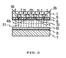
- a discharge cell 2 comprises four electrodes formed on a first glass substrate 1. Two of them are scanning electrodes 3b and 3c provided at one side, and the other two of them are maintaining electrodes 4b and 4c provided at another side. These electrodes are covered with a dielectric layer 5 and a protective film layer 6.
- a plurality of ribs 9 are arranged orthogonally to the scanning electrode 3b and 3c and the maintaining electrodes 4b and 4c.
- a data electrode 8 is arranged between two ribs 9 formed on the surface of the second glass substrate 7 and is parallel to the ribs.
- a phosphor layer 10 is formed between these two ribs on the surface of the data electrode 8.
- a discharge space 11 is defined by a first glass substrate 1, a second glass substrate 7, and ribs 9.
- a discharge cell 2 is formed, where a pair of electrodes consisting of a scanning electrode 3b and 3c, a maintaining electrode 4b and 4c, and two ribs are crossing.
- a scanning electrode 3b and 3c, a maintaining electrode 4b and 4c and a data electrode 8 are composed of Ag or a laminated conductor in which a Cu layer is sandwiched by Cr layers.
- a dielectric layer 5 is composed of borosilicate glass and the like, and a protective film layer 6 is composed of MgO and the like. At least one of a noble gas such as helium, neon, argon or xenon is sealed in the discharge space 11.
- FIG. 2 is a sectional view of a discharge cell 2 taken on line II-II of FIG. 1.
- a positive write pulse is applied to a data electrode 8 and a negative scanning pulse voltage is applied to a scanning electrode 3b and 3c. Consequently, a write discharge is occured in discharge space 11, and therefore a positive electrical charge is stored on the surface of a protective film layer 6 formed on the scanning electrode 3b and 3c.
- a negative maintaining pulse voltage is applied to maintaining electrodes 4b and 4c, and consequently a maintaining discharge is excited by the positive electrical discharge generated on the surface of the protective film layer 6 formed on the scanning electrodes 3b and 3c.
- the maintaining discharge is continued by applying a negative maintaining pulse voltage to the scanning electrodes 3b and 3c and the maintaining electrodes 4b and 4c alternately.
- the maintaining discharge is ceased by applying a negative erasing pulse voltage to the maintaining electrode 4b and 4c.
- the maintaining discharge is generated between two scanning electrodes 3b and 3c, and two maintaining electrodes 4b and 4c.
- a width of each electrode d is set to be half of a width of an electrode of conventional case, that is, d 0 /2
- a distance W between a scanning electrode 3c and a maintaining electrode 4b is identical to that of the conventional case, and a distance between each scanning electrode and between each maintaining electrode is set to be g
- the distance between the right side end of the scanning electrode 3b and the left side end of the maintaining electrode 4c as shown in FIG. 2 is widened, that is, a length of 2 x g is added to the distance of the conventional example as shown in FIG. 11.
- a maintaining discharge region S of this embodiment of this invention is widened, that is, a length of 2 x g is added, in comparison with the maintaining discharge region S of the conventional example. Consequently, the widened discharge region is equivalent to a discharge region between a scanning electrode whose width is the sum of d 0 and g and a maintaining electrodes whose width is the sum of d 0 and g.
- the area of the electrodes which interrupts a visible light is the same as that of the conventional example, therefore the opening ratio becomes the same as that of the conventional type.
- a discharge region S can be widened without decreasing the opening ratio, and therefore a brightness can be improved.
- the distance W between a scanning electrode 3c and a maintaining electrode 4b is widened, a luminous efficiency of the maintaining discharge can be improved.
- a maintaining discharge voltage is increased considerably. Therefore, the distance W is set to be in a range between 20 ⁇ m and 200 ⁇ m, taking into consideration the requirements of practical use.
- the width d of a scanning electrode 3b and 3c, a maintaining electrode 4b and 4c, of an AC plasma display panel is set to be dm/2 to compare with a conventional example of AC plasma display panel under the same conditions.
- dm/2 x 4 is equivalent to dm x 2
- a ratio of visible light, emitting from a phosphor layer 10 which is interrupted by a width of the scanning electrode 3b and 3c the maintaining electrode 4b and 4c becomes the same, that is the opening ratio of the panel becomes the same as that of the conventional example.
- the discharge condition becomes the same as a case in which a width of a scanning electrode and a maintaining electrode is widened as shown in FIG. 12.
- the maintaining discharge region S in the discharge cell 2 is widened, a large amount of ultraviolet rays can be obtained, and consequently, the amount of visible light emitted from phosphor layer 10 is increased.
- the ratio of the visible light which is interrupted by the width of scanning electrodes 3b and 3c and maintaining electrodes 4b and 4c is the same as that of conventional example even if the distance g is widened. Therefore, the opening ratio A of the panel is constant, and a brightness is increased with an extension of the region S.
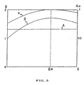
- FIG. 3 is a graph showing the relationship between a distance, g, between scanning electrodes 3b and 3c and maintaining electrodes 4b and 4c, an amount of ultraviolet rays, u, opening ratio A of the panel and the brightness B of the panel.
- the scale used in FIG. 3 is a relative scale.
- g is 0, the values of B, u and A are equivalent to the values of B, u and A of the conventional example when d is dm as shown in FIG. 13.
- the results shown in FIG.3 when g is gm, the brightness B of panel becomes maximum.
- the gm satisfies two conditions, such as d + gm is in a range between 200 ⁇ m and 2000 ⁇ m, and gm is in a range between d/2 and d.
- the brightness B of panel becomes about 1.7 times the value of the conventional example as shown in FIG. 13.
- dm satisfies two conditions, such as dm+W is in a range between 200 ⁇ m and 2000 ⁇ m, and dm is in a range between p/5 and p/3.
- the width of an electrode of this embodiment, d is dm/2. Therefore when dm of the above-mentioned formula is substituted by 2d, the width of the electrode d satisfies two conditions such as 2d + W is in a range between 200 ⁇ m and 2000 ⁇ m, and 2d is in a range between p/5 and p/3. In this case, W is in a range between 20 ⁇ m and 200 ⁇ m.
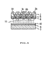
- a discharge cell 2 formed on a first glass substrate comprises a group of electrodes in which a scanning electrode 3b, a maintaining electrode 4b, a scanning electrode 3c and a maintaining electrode 4c are arranged in that order. That is, a scanning electrode and a maintaining electrode are arranged alternately.
- FIG. 5 is a sectional view taken on line V-V of a discharge cell of FIG. 4. A distance h between a scanning electrode 3c and a maintaining electrode 4b is set when W is in a range between 20 ⁇ m and 200 ⁇ m.
- the width of a scanning electrode 3b, 3c and a maintaining electrode 4b and 4c, d is set to be dm/2.
- a distance h is widened, one discharge is generated at a region Sa by a scanning electrode 3b and a maintaining electrode 4b, and another discharge is generated at a region Sb by a scanning electrode 3c and a maintaining electrode 4c.
- a discharge cell 2 two maintaining discharge are generated at regions, Sa and Sb, a large amount of ultraviolet rays can be obtained and an amount of visible light emitted from the phosphor layer 10 is increased.
- the area of the scanning electrodes 3c, 3b and the maintaining electrodes 4b and 4c that interrupt the visible light are not changed. Consequently, the opening ratio A of panel is constant and the luminous brightness of the panel increases with a increase of the ultraviolet rays.
- FIG. 6 is a graph showing the relationship between the distance h, the amount of ultraviolet rays u, the numerical aperture A of the panel and the brightness B of panel.
- the scale used in FIG. 6 is a relative scale, which is the same as that used in FIG. 3.
- the brightness of panel B becomes maximum.
- the hm is in a range between (d+W)/3 and (d+W)/2.
- the luminous brightness B of panel becomes 1.4 times the value of the conventional example as shown in FIG. 10.
- dm satisfies two conditions, such as dm+W is in a range between 200 ⁇ m and 2000 ⁇ m, and dm is in a range between p/5 and p/3.
- the width of an electrode of this embodiment, d is dm/2, therefore when dm of the above-mentioned formula is substituted by 2d, the width of the electrode d satisfies two conditions such as 2d + W is in a range between 200 ⁇ m and 2000 ⁇ m, and 2d is in a range between p/5 and p/3. In this case, W is in a range between 20 ⁇ m and 200 ⁇ m.
- a discharge cell comprises two scanning electrodes and two maintaining electrodes.
- the same effect can be obtained by arranging a pair or a plurality of pairs of electrodes consisting of a plurality of scanning electrodes at one side, and a plurality of maintaining electrodes whose number is the same as that of scanning electrodes at another side in a discharge cell 2.
- the same effect can be obtained by arranging a plurality of pairs of electrodes consisting of a scanning electrode and a maintaining electrode in which a position of the scanning electrode and the maintaining electrode are arranged alternately.
- the same effect can be obtained by arranging a pair or a plurality of pairs of electrodes consisting of four electrodes in which two scanning electrodes are arranged at outside and two maintaining electrodes are arranged at the inside in a discharge cell 2.
- an arrangement of electrodes may be reversed, that is, two maintaining electrodes may be arranged at outside ends and two scanning electrodes may be arranged at the inside.
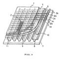
- FIG. 8 is a sectional view showing again a discharge cell 2 taken on line II-II of FIG. 1 with reference numerals according to Figs. 7 and 9.
- two scanning electrodes 3b and 3c, and two maintaining electrodes 4b and 4c are positioned separately. Consequently, at an initial stage of discharge, an electric field tends to be focused on the region between a pair of electrodes consisting of a scanning electrode 3c and a maintaining electrode 4c. Therefore, even at a final stage of discharge, the discharge of a discharge cell is limited to a narrow region Sa, and on the other hand, the discharge of a discharge cell is widened to region Sb.
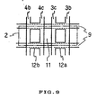
- a discharge cell 2 comprises a group of four electrodes consisting of two scanning electrodes 3b and 3c arranged at one side, and two maintaining electrodes 4b and 4c arranged at another side and these two scanning electrodes 3b and 3c are connected electrically via a plurality of induction electrodes 12a at a position of rib 9, in the same way, these maintaining electrodes 4b and 4c are connected electrically via a plurality of induction electrodes 12b at a position of rib 9.
- FIG. 9 is a plan view showing a scanning electrode and a maintaining electrode.
- the width of the induction electrode 12a and 12b is set to be slightly wider than that of a rib 9, and therefore, a portion of the induction electrode is exposed to a discharge space 11. Consequently, an electric field between a scanning electrode 3c and a maintaining electrode 4c is equalized to an electric field between a scanning electrode 3b and a maintaining electrode 4b by the presence of the exposed portion of induction electrode 12a and 12b.
- a discharge region is not limited to a narrow region Sa, and a reduction of brightness of panel and a brightness irregurality on the display panel can be prevented.
- the discharge cell comprises two scanning electrodes and two maintaining electrodes, however, the same effect can be obtained by a discharge cell comprising more than three scanning electrodes and maintaining electrodes.
- a pair of electrodes consisting of a scanning electrode and a maintaining electrodes are arranged, however, the same effect can be obtained by arranging a plurality of pairs of electrodes consisting of a scanning electrode and a maintaining electrode.
Landscapes
- Engineering & Computer Science (AREA)
- Physics & Mathematics (AREA)
- Plasma & Fusion (AREA)
- Chemical & Material Sciences (AREA)
- Materials Engineering (AREA)
- Gas-Filled Discharge Tubes (AREA)
Claims (5)
- Wechselstrom-Plasmaanzeigetafel, die folgendes umfaßt:ein erstes (1) und zweites Glassubstrat (7), die einander zugewandt sind und zwischen sich einen Entladungsraum (11) definieren,mehrere abtastende Elektroden (3b, 3c) und aufrechterhaltende Elektroden (4b, 4c), die parallel zueinander verlaufen und auf dem ersten Glassubstrat (1) ausgebildet sind,eine dielektrische Schicht (5), die die abtastenden Elektroden (3b, 3c) und die aufrechterhaltenden Elektroden (4b, 4c) bedeckt, undmehrere Rippen (9) und Datenelektroden (8), die auf dem zweiten Glassubstrat (7) ausgebildet und orthogonal zu den abtastenden Elektroden (3b, 3c) und den aufrechterhaltenden Elektroden (4b, 4c) angeordnet sind,wobei eine Entladungszelle (2), die durch Unterteilung des Entladungsraums durch ein Paar benachbarte Rippen (9) gebildet wird, mehrere abtastende Elektroden (3b, 3c) und aufrechterhaltende Elektroden (4b, 4c) umfaßt,dadurch gekennzeichnet, daß die abtastenden Elektroden (3b, 3c) und die aufrechterhaltenden Elektroden (4b, 4c) für sichtbares Licht undurchlässig sind und das erste Glassubstrat (1) an der Seite des Displays vorgesehen ist,die Entladungszelle (2) vier Elektroden umfaßt, von denen zwei abtastende Elektroden (3b, 3c) auf einer Seite jeder Entladungszelle (2) und zwei aufrechterhaltende Elektroden (4b, 4c) auf einer anderen Seite jeder Entladungszelle (2) vorgesehen sind,eine Entfernung W zwischen einer Kante einer abtastenden Elektrode (3b, 3c) und einer Kante einer benachbarten aufrechterhaltenden Elektrode (4b, 4c) in einem Bereich zwischen 20 µm und 200 µm liegt,eine Breite jeder Elektrode als d und eine Breite einer Entladungszelle (2) als p gezeigt ist und 2d den Bedingungen genügt, daß 2d + W in einem Bereich zwischen 200 µm und 2000 µm und 2d in einem Bereich zwischen p/5 und p/3 liegt, undeine Entfernung zwischen einer Kante einer abtastenden Elektrode (z.B. 3b) und einer Kante einer benachbarten Elektrode (z.B. 3c) als g gezeigt ist, wobei g den Bedingungen genügt, daß d + g in einem Bereich zwischen 200 µm und 2000 µm und g in einem Bereich zwischen d/2 und d liegt.
- Wechselstrom-Plasmaanzeigetafel, die folgendes umfaßt:ein erstes (1) und zweites Glassubstrat (7), die einander zugewandt sind und zwischen sich einen Entladungsraum (11) definieren,mehrere abtastende Elektroden (3b, 3c) und aufrechterhaltende Elektroden (4b, 4c), die parallel zueinander verlaufen und auf dem ersten Glassubstrat (1) ausgebildet sind,eine dielektrische Schicht (5), die die abtastenden Elektroden (3b, 3c) und die aufrechterhaltenden Elektroden (4b, 4c) bedeckt, undmehrere Rippen (9) und Datenelektroden (8), die auf dem zweiten Glassubstrat (7) ausgebildet und orthogonal zu den abtastenden Elektroden (3b, 3c) und den aufrechterhaltenden Elektroden (4b, 4c) angeordnet sind,wobei eine Entladungszelle (2), die durch Unterteilung des Entladungsraums durch ein Paar benachbarte Rippen (9) gebildet wird, mehrere abtastende Elektroden (3b, 3c) und aufrechterhaltende Elektroden (4b, 4c) umfaßt,dadurch gekennzeichnet, daß die abtastenden Elektroden (3b, 3c) und die aufrechterhaltenden Elektroden (4b, 4c) für sichtbares Licht undurchlässig sind und das erste Glassubstrat (1) an der Seite des Displays vorgesehen ist,die Entladungszelle (2) zwei Paar Elektroden umfaßt, wobei jedes Paar aus einer abtastenden Elektrode (z.B. 3b) und einer aufrechterhaltenden Elektrode (z.B. 4b) besteht und die abtastenden Elektroden (3b, 3c) und die aufrechterhaltenden Elektroden (4b, 4c) abwechselnd positioniert sind,für das Paar Elektroden eine Entfernung W zwischen einer Kante der abtastenden Elektrode (z.B. 3b) und einer Kante der benachbarten aufrechterhaltenden Elektrode (z.B. 4b) in einem Bereich zwischen 20 µm und 200 µm liegt,eine Breite jeder abtastenden Elektrode (3b, 3c) und aufrechterhaltenden Elektrode (4b, 4c) als d und eine Breite einer Entladungszelle (2) als p gezeigt ist und 2d den Bedingungen genügt, daß 2d + W in einem Bereich zwischen 200 µm und 2000 µm und 2d in einem Bereich zwischen p/5 und p/3 liegt, undeine Innenentfernung h zwischen einer Kante einer abtastenden Elektrode (z.B. 3c) und einer Kante einer benachbarten aufrechterhaltenden Elektrode (z.B. 4b) in einem Bereich zwischen (d + W)/3 und (d + W)/2 liegt.
- Wechselstrom-Plasmaanzeigetafel, die folgendes umfaßt:ein erstes (1) und zweites Glassubstrat (7), die einander zugewandt sind und zwischen sich einen Entladungsraum (11) definieren,mehrere abtastende Elektroden (3b, 3c) und aufrechterhaltende Elektroden (4b, 4c), die parallel zueinander verlaufen und auf dem ersten Glassubstrat (1) ausgebildet sind,eine dielektrische Schicht (5), die die abtastenden Elektroden (3b, 3c) und die aufrechterhaltenden Elektroden (4b, 4c) bedeckt, undmehrere Rippen (9) und Datenelektroden (8), die auf dem zweiten Glassubstrat (7) ausgebildet und orthogonal zu den abtastenden Elektroden (3b, 3c) und den aufrechterhaltenden Elektroden (4b, 4c) angeordnet sind,wobei eine Entladungszelle (2), die durch Unterteilung des Entladungsraums durch ein Paar benachbarte Rippen (9) gebildet wird, mehrere abtastende Elektroden (3b, 3c) und aufrechterhaltende Elektroden (4b, 4c) umfaßt,dadurch gekennzeichnet, daß die abtastenden Elektroden (3b, 3c) und die aufrechterhaltenden Elektroden (4b, 4c) für sichtbares Licht undurchlässig sind und das erste Glassubstrat (1) an der Seite des Displays vorgesehen ist,die Entladungszelle (2) mehrere auf einer Seite einer Entladungszelle (2) angeordnete abtastende Elektroden (3b, 3c) umfaßt und die gleiche Anzahl an aufrechterhaltenden Elektroden (4b, 4c) wie die der abtastenden Elektroden (3b, 3c) auf einer anderen Seite der Entladungszelle (2) angeordnet ist und mehrere elektrisch mit den mehreren abtastenden Elektroden (3b, 3c) verbundene Induktionselektroden (12a) auf einer Seite der Entladungszelle (2) an einer Position einer Rippe (9) und mehrere elektrisch mit den mehreren aufrechterhaltenden Elektroden (4b, 4c) verbundene Induktionselektroden (12b) auf einer anderen Seite der Entladungszelle (2) an einer Position der Rippe (9) vorgesehen sind, wobei ein Teil der Induktionselektroden (12a, b) zum Entladungsraum (11) hin offen ist.
- Wechselstrom-Plasmaanzeigetafel nach Anspruch 1, 2 oder 3, wobei die aufrechterhaltenden Elektroden (4b, 4c) und die Datenelektrode (8) aus Ag oder aus einem lamininierten Leiter bestehen, bei dem eine Cu-Schicht zwischen Cr-Schichten geschichtet ist.
- Wechselstrom-Plasmaanzeigetafel nach Anspruch 1, 2 oder 3, wobei ein Edelgas in den Entladungsraum (11) eingeschlossen ist.
Applications Claiming Priority (3)
| Application Number | Priority Date | Filing Date | Title |
|---|---|---|---|
| JP95703/96 | 1996-04-17 | ||
| JP9570396 | 1996-04-17 | ||
| JP8095703A JPH09283028A (ja) | 1996-04-17 | 1996-04-17 | Ac型プラズマディスプレイパネル |
Publications (3)
| Publication Number | Publication Date |
|---|---|
| EP0802556A2 EP0802556A2 (de) | 1997-10-22 |
| EP0802556A3 EP0802556A3 (de) | 1998-11-04 |
| EP0802556B1 true EP0802556B1 (de) | 2002-11-13 |
Family
ID=14144873
Family Applications (1)
| Application Number | Title | Priority Date | Filing Date |
|---|---|---|---|
| EP97105986A Expired - Lifetime EP0802556B1 (de) | 1996-04-17 | 1997-04-11 | Wechselstrom-Plasma-Anzeigetafel |
Country Status (7)
| Country | Link |
|---|---|
| US (1) | US5841232A (de) |
| EP (1) | EP0802556B1 (de) |
| JP (1) | JPH09283028A (de) |
| KR (2) | KR100259794B1 (de) |
| CN (1) | CN1074581C (de) |
| DE (1) | DE69716985T2 (de) |
| TW (1) | TW507240B (de) |
Families Citing this family (23)
| Publication number | Priority date | Publication date | Assignee | Title |
|---|---|---|---|---|
| JPH10321145A (ja) * | 1997-03-19 | 1998-12-04 | Sony Corp | 表示装置 |
| JP3635881B2 (ja) * | 1997-08-01 | 2005-04-06 | 松下電器産業株式会社 | プラズマディスプレイパネル |
| EP0923106A1 (de) * | 1997-12-11 | 1999-06-16 | Corning Incorporated | Elektroden für elektronische Anzeige |
| JPH11282378A (ja) | 1998-03-26 | 1999-10-15 | Sony Corp | カラープロジェクタ |
| JP2000357462A (ja) * | 1998-10-23 | 2000-12-26 | Sony Corp | 平面型プラズマ放電表示装置と駆動方法 |
| JP3470629B2 (ja) * | 1999-02-24 | 2003-11-25 | 富士通株式会社 | 面放電型プラズマディスプレイパネル |
| US6411035B1 (en) * | 1999-05-12 | 2002-06-25 | Robert G. Marcotte | AC plasma display with apertured electrode patterns |
| US6680573B1 (en) * | 1999-07-26 | 2004-01-20 | Lg Electronics Inc. | Plasma display panel with improved illuminance |
| JP2001160361A (ja) * | 1999-09-21 | 2001-06-12 | Mitsubishi Electric Corp | プラズマディスプレイパネル用基板及びプラズマディスプレイパネル |
| US6980178B2 (en) | 1999-12-16 | 2005-12-27 | Lg Electronics Inc. | Method of driving plasma display panel |
| KR100880774B1 (ko) * | 2000-01-25 | 2009-02-02 | 파나소닉 주식회사 | 가스방전패널 |
| CN100409394C (zh) * | 2000-08-29 | 2008-08-06 | 松下电器产业株式会社 | 气体放电屏 |
| FR2819097B1 (fr) * | 2001-01-02 | 2003-04-11 | Thomson Plasma | Structure d'electrodes de maintien pour dalle avant de panneau de visualisation a plasma |
| JP2003068208A (ja) * | 2001-08-28 | 2003-03-07 | Matsushita Electric Ind Co Ltd | プラズマディスプレイパネルおよびその駆動方法 |
| FR2841378A1 (fr) * | 2002-06-24 | 2003-12-26 | Thomson Plasma | Dalle de decharges coplanaires pour panneau de visualisation a plasma apportant une distribution de potentiel de surface adaptee |
| CN1319105C (zh) * | 2003-05-21 | 2007-05-30 | 中华映管股份有限公司 | 电浆显示面板 |
| JP2005031479A (ja) * | 2003-07-08 | 2005-02-03 | Nec Plasma Display Corp | プラズマディスプレイ装置及びその駆動方法 |
| EP1530191A3 (de) * | 2003-11-07 | 2008-02-27 | Thomson Plasma S.A.S. | Plasmaanzeigetafel mit kleinem Abstand und langgestreckten koplanaren Entladungen |
| KR100589338B1 (ko) * | 2004-04-07 | 2006-06-14 | 삼성에스디아이 주식회사 | 어드레스 전극간 캐패시턴스를 낮춘 플라즈마 디스플레이패널 |
| KR100658711B1 (ko) * | 2004-04-08 | 2006-12-15 | 삼성에스디아이 주식회사 | 플라즈마 디스플레이 패널 |
| KR100730143B1 (ko) * | 2005-08-30 | 2007-06-19 | 삼성에스디아이 주식회사 | 전극 단자부 구조 및 이를 구비한 플라즈마 디스플레이패널 |
| EP1770750A3 (de) * | 2005-09-30 | 2009-03-11 | Lg Electronics Inc. | Plasma-Bildschirm |
| KR20230018242A (ko) * | 2021-07-29 | 2023-02-07 | 엘지이노텍 주식회사 | 회로기판 및 이를 포함하는 패키지 기판 |
Family Cites Families (6)
| Publication number | Priority date | Publication date | Assignee | Title |
|---|---|---|---|---|
| JP3242938B2 (ja) * | 1991-05-07 | 2001-12-25 | 富士通株式会社 | プラズマディスプレイパネル |
| EP0554172B1 (de) * | 1992-01-28 | 1998-04-29 | Fujitsu Limited | Plasma Farbanzeige-Vorrichtung von Oberflächenentladungs-Typ |
| JPH07111134A (ja) * | 1993-10-13 | 1995-04-25 | Oki Electric Ind Co Ltd | ガス放電表示パネル及びその電極形成方法 |
| US5684499A (en) * | 1993-11-29 | 1997-11-04 | Nec Corporation | Method of driving plasma display panel having improved operational margin |
| US5656893A (en) * | 1994-04-28 | 1997-08-12 | Matsushita Electric Industrial Co., Ltd. | Gas discharge display apparatus |
| JP3466346B2 (ja) * | 1995-10-26 | 2003-11-10 | 株式会社日立製作所 | プラズマディスプレイパネルの電極構造 |
-
1996
- 1996-04-17 JP JP8095703A patent/JPH09283028A/ja active Pending
-
1997
- 1997-04-09 US US08/833,759 patent/US5841232A/en not_active Expired - Lifetime
- 1997-04-11 DE DE69716985T patent/DE69716985T2/de not_active Expired - Lifetime
- 1997-04-11 EP EP97105986A patent/EP0802556B1/de not_active Expired - Lifetime
- 1997-04-12 TW TW086104705A patent/TW507240B/zh active
- 1997-04-17 KR KR1019970014281A patent/KR100259794B1/ko not_active Expired - Fee Related
- 1997-04-17 CN CN97110575A patent/CN1074581C/zh not_active Expired - Fee Related
-
2000
- 2000-01-25 KR KR1020000003415A patent/KR100374968B1/ko not_active Expired - Fee Related
Also Published As
| Publication number | Publication date |
|---|---|
| DE69716985D1 (de) | 2002-12-19 |
| KR100374968B1 (ko) | 2003-03-06 |
| US5841232A (en) | 1998-11-24 |
| KR100259794B1 (ko) | 2000-06-15 |
| TW507240B (en) | 2002-10-21 |
| CN1167330A (zh) | 1997-12-10 |
| EP0802556A2 (de) | 1997-10-22 |
| EP0802556A3 (de) | 1998-11-04 |
| KR970071949A (ko) | 1997-11-07 |
| JPH09283028A (ja) | 1997-10-31 |
| CN1074581C (zh) | 2001-11-07 |
| DE69716985T2 (de) | 2003-07-03 |
Similar Documents
| Publication | Publication Date | Title |
|---|---|---|
| EP0802556B1 (de) | Wechselstrom-Plasma-Anzeigetafel | |
| KR100758681B1 (ko) | 플라즈마 디스플레이 패널의 전극 구조 | |
| US6384531B1 (en) | Plasma display device with conductive metal electrodes and auxiliary electrodes | |
| KR100483245B1 (ko) | 플라즈마표시패널 및 플라즈마표시패널 제조방법 | |
| JP3698856B2 (ja) | プラズマディスプレイパネル | |
| CN1269571A (zh) | 等离子体显示装置及具有集中电场区域的介电层的制作方法 | |
| US5962974A (en) | Face-discharge AC driving plasma display panel | |
| US6768261B2 (en) | Transmission type color plasma display panel | |
| US6043605A (en) | Plasma display device with auxiliary electrodes and protective layer | |
| KR100263854B1 (ko) | 플라즈마 표시장치 | |
| US7852003B2 (en) | Plasma display panel having dimension relationship between width of electrodes and barrier rib pitch | |
| JP2705599B2 (ja) | プラズマディスプレイパネル | |
| KR100769789B1 (ko) | 플라즈마 디스플레이 패널 | |
| KR100416145B1 (ko) | 플라즈마 디스플레이 패널 | |
| KR19990056758A (ko) | 플라즈마 디스플레이 패널 | |
| US7183709B2 (en) | Plasma display panel having electrodes having identical pitch in the display region and the terminal regions | |
| US6437514B1 (en) | AC plasma display device | |
| KR100441515B1 (ko) | 플라즈마 디스플레이 패널 | |
| KR100362057B1 (ko) | 플라즈마 디스플레이 패널 | |
| US7560864B2 (en) | Plasma display panel having slanted electrodes embedded in dielectric partition walls | |
| KR20050111907A (ko) | 플라즈마 디스플레이 패널 | |
| KR100647644B1 (ko) | 플라즈마 디스플레이 패널 | |
| JP2003092063A (ja) | プラズマディスプレイパネル | |
| EP1788609A2 (de) | Plasmaanzeigetafel mit höherem Integrationsgrad der Pixel | |
| KR100322074B1 (ko) | 플라즈마 디스플레이 패널 |
Legal Events
| Date | Code | Title | Description |
|---|---|---|---|
| PUAI | Public reference made under article 153(3) epc to a published international application that has entered the european phase |
Free format text: ORIGINAL CODE: 0009012 |
|
| AK | Designated contracting states |
Kind code of ref document: A2 Designated state(s): DE FR GB IT |
|
| PUAL | Search report despatched |
Free format text: ORIGINAL CODE: 0009013 |
|
| AK | Designated contracting states |
Kind code of ref document: A3 Designated state(s): DE FR GB IT |
|
| 17P | Request for examination filed |
Effective date: 19990430 |
|
| 17Q | First examination report despatched |
Effective date: 20010712 |
|
| RAP1 | Party data changed (applicant data changed or rights of an application transferred) |
Owner name: MATSUSHITA ELECTRIC INDUSTRIAL CO., LTD. |
|
| GRAG | Despatch of communication of intention to grant |
Free format text: ORIGINAL CODE: EPIDOS AGRA |
|
| GRAG | Despatch of communication of intention to grant |
Free format text: ORIGINAL CODE: EPIDOS AGRA |
|
| GRAH | Despatch of communication of intention to grant a patent |
Free format text: ORIGINAL CODE: EPIDOS IGRA |
|
| GRAH | Despatch of communication of intention to grant a patent |
Free format text: ORIGINAL CODE: EPIDOS IGRA |
|
| GRAA | (expected) grant |
Free format text: ORIGINAL CODE: 0009210 |
|
| AK | Designated contracting states |
Kind code of ref document: B1 Designated state(s): DE FR GB IT |
|
| REG | Reference to a national code |
Ref country code: GB Ref legal event code: FG4D |
|
| REF | Corresponds to: |
Ref document number: 69716985 Country of ref document: DE Date of ref document: 20021219 |
|
| ET | Fr: translation filed | ||
| PLBE | No opposition filed within time limit |
Free format text: ORIGINAL CODE: 0009261 |
|
| STAA | Information on the status of an ep patent application or granted ep patent |
Free format text: STATUS: NO OPPOSITION FILED WITHIN TIME LIMIT |
|
| 26N | No opposition filed |
Effective date: 20030814 |
|
| REG | Reference to a national code |
Ref country code: GB Ref legal event code: 746 Effective date: 20100127 |
|
| PGFP | Annual fee paid to national office [announced via postgrant information from national office to epo] |
Ref country code: DE Payment date: 20110406 Year of fee payment: 15 Ref country code: FR Payment date: 20110426 Year of fee payment: 15 |
|
| PGFP | Annual fee paid to national office [announced via postgrant information from national office to epo] |
Ref country code: GB Payment date: 20110406 Year of fee payment: 15 |
|
| PGFP | Annual fee paid to national office [announced via postgrant information from national office to epo] |
Ref country code: IT Payment date: 20110420 Year of fee payment: 15 |
|
| GBPC | Gb: european patent ceased through non-payment of renewal fee |
Effective date: 20120411 |
|
| REG | Reference to a national code |
Ref country code: FR Ref legal event code: ST Effective date: 20121228 |
|
| PG25 | Lapsed in a contracting state [announced via postgrant information from national office to epo] |
Ref country code: GB Free format text: LAPSE BECAUSE OF NON-PAYMENT OF DUE FEES Effective date: 20120411 |
|
| REG | Reference to a national code |
Ref country code: DE Ref legal event code: R119 Ref document number: 69716985 Country of ref document: DE Effective date: 20121101 |
|
| PG25 | Lapsed in a contracting state [announced via postgrant information from national office to epo] |
Ref country code: IT Free format text: LAPSE BECAUSE OF NON-PAYMENT OF DUE FEES Effective date: 20120411 Ref country code: FR Free format text: LAPSE BECAUSE OF NON-PAYMENT OF DUE FEES Effective date: 20120430 |
|
| PG25 | Lapsed in a contracting state [announced via postgrant information from national office to epo] |
Ref country code: DE Free format text: LAPSE BECAUSE OF NON-PAYMENT OF DUE FEES Effective date: 20121101 |