EP0802571A3 - Semiconductor device comprising a field effect transistor and process of fabrication - Google Patents
Semiconductor device comprising a field effect transistor and process of fabrication Download PDFInfo
- Publication number
- EP0802571A3 EP0802571A3 EP97106579A EP97106579A EP0802571A3 EP 0802571 A3 EP0802571 A3 EP 0802571A3 EP 97106579 A EP97106579 A EP 97106579A EP 97106579 A EP97106579 A EP 97106579A EP 0802571 A3 EP0802571 A3 EP 0802571A3
- Authority
- EP
- European Patent Office
- Prior art keywords
- source
- drain
- effect transistor
- electrode
- einer
- Prior art date
- Legal status (The legal status is an assumption and is not a legal conclusion. Google has not performed a legal analysis and makes no representation as to the accuracy of the status listed.)
- Withdrawn
Links
Classifications
-
- H—ELECTRICITY
- H10—SEMICONDUCTOR DEVICES; ELECTRIC SOLID-STATE DEVICES NOT OTHERWISE PROVIDED FOR
- H10F—INORGANIC SEMICONDUCTOR DEVICES SENSITIVE TO INFRARED RADIATION, LIGHT, ELECTROMAGNETIC RADIATION OF SHORTER WAVELENGTH OR CORPUSCULAR RADIATION
- H10F30/00—Individual radiation-sensitive semiconductor devices in which radiation controls the flow of current through the devices, e.g. photodetectors
- H10F30/20—Individual radiation-sensitive semiconductor devices in which radiation controls the flow of current through the devices, e.g. photodetectors the devices having potential barriers, e.g. phototransistors
- H10F30/21—Individual radiation-sensitive semiconductor devices in which radiation controls the flow of current through the devices, e.g. photodetectors the devices having potential barriers, e.g. phototransistors the devices being sensitive to infrared, visible or ultraviolet radiation
- H10F30/28—Individual radiation-sensitive semiconductor devices in which radiation controls the flow of current through the devices, e.g. photodetectors the devices having potential barriers, e.g. phototransistors the devices being sensitive to infrared, visible or ultraviolet radiation the devices being characterised by field-effect operation, e.g. junction field-effect phototransistors
-
- H—ELECTRICITY
- H10—SEMICONDUCTOR DEVICES; ELECTRIC SOLID-STATE DEVICES NOT OTHERWISE PROVIDED FOR
- H10F—INORGANIC SEMICONDUCTOR DEVICES SENSITIVE TO INFRARED RADIATION, LIGHT, ELECTROMAGNETIC RADIATION OF SHORTER WAVELENGTH OR CORPUSCULAR RADIATION
- H10F71/00—Manufacture or treatment of devices covered by this subclass
Landscapes
- Junction Field-Effect Transistors (AREA)
Abstract
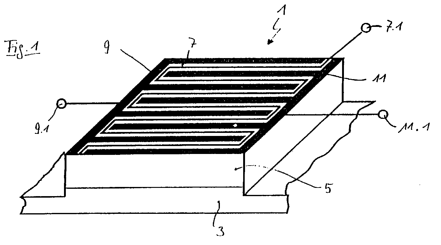
In einem Halbleiter-Bauelement mit einem Substrat und mit einem auf dem Substrat ausgebildeten Feldeffekttransistor bzw. in einem Feldeffekttransistor, bei dem ein durch einen leitenden Halbleiterkanal zwischen einer Sourceelektrode und einer Drainelektrode fließender Strom über ein senkrecht auf den Kanal einwirkendes Feld zwischen einer einzelnen Gateelektrode und dem Kanal steuerbar ist und der eine relativ große aktive Transistorfläche aufweist, sind die Sourceelektrode (9, 9.1), die Drainelektrode (11, 11.1) und die Gateelektrode (7, 7.1) überkreuzungsfrei ausgebildet.In a semiconductor device with a substrate and with one on the Field-effect transistor formed in the substrate or in a field-effect transistor, in which a through a conductive semiconductor channel between one Source electrode and a drain electrode current flowing through a perpendicular field acting on the channel between a single gate electrode and the channel is controllable and a relatively large active transistor area has, the source electrode (9, 9.1), the drain electrode (11, 11.1) and the gate electrode (7, 7.1) is designed so that it does not cross.
Ein. Verfahren zur Herstellung eines Halbleiter-Bauelementes mit einem
Feldeffekttransistor umfaßt die Schritte
Applications Claiming Priority (2)
| Application Number | Priority Date | Filing Date | Title |
|---|---|---|---|
| DE19615495 | 1996-04-19 | ||
| DE19615495A DE19615495C2 (en) | 1996-04-19 | 1996-04-19 | Semiconductor component and method for its production |
Publications (2)
| Publication Number | Publication Date |
|---|---|
| EP0802571A2 EP0802571A2 (en) | 1997-10-22 |
| EP0802571A3 true EP0802571A3 (en) | 1998-10-21 |
Family
ID=7791748
Family Applications (1)
| Application Number | Title | Priority Date | Filing Date |
|---|---|---|---|
| EP97106579A Withdrawn EP0802571A3 (en) | 1996-04-19 | 1997-04-21 | Semiconductor device comprising a field effect transistor and process of fabrication |
Country Status (2)
| Country | Link |
|---|---|
| EP (1) | EP0802571A3 (en) |
| DE (1) | DE19615495C2 (en) |
Cited By (1)
| Publication number | Priority date | Publication date | Assignee | Title |
|---|---|---|---|---|
| US7939866B2 (en) | 2007-05-21 | 2011-05-10 | Rfmd (Uk) Limited | Field effect transistor |
Families Citing this family (2)
| Publication number | Priority date | Publication date | Assignee | Title |
|---|---|---|---|---|
| KR100864918B1 (en) * | 2001-12-26 | 2008-10-22 | 엘지디스플레이 주식회사 | Data driving device of liquid crystal display |
| DE102011075103B4 (en) | 2011-05-02 | 2014-04-10 | Forschungsverbund Berlin E.V. | photodetector |
Citations (3)
| Publication number | Priority date | Publication date | Assignee | Title |
|---|---|---|---|---|
| US4351706A (en) * | 1980-03-27 | 1982-09-28 | International Business Machines Corporation | Electrochemically eroding semiconductor device |
| EP0373803A2 (en) * | 1988-12-16 | 1990-06-20 | Raytheon Company | R. F. switching circuits |
| US5453630A (en) * | 1992-11-12 | 1995-09-26 | The United States Of America As Represented By The Secretary Of The Army | Variable gain optical detector |
-
1996
- 1996-04-19 DE DE19615495A patent/DE19615495C2/en not_active Expired - Fee Related
-
1997
- 1997-04-21 EP EP97106579A patent/EP0802571A3/en not_active Withdrawn
Patent Citations (3)
| Publication number | Priority date | Publication date | Assignee | Title |
|---|---|---|---|---|
| US4351706A (en) * | 1980-03-27 | 1982-09-28 | International Business Machines Corporation | Electrochemically eroding semiconductor device |
| EP0373803A2 (en) * | 1988-12-16 | 1990-06-20 | Raytheon Company | R. F. switching circuits |
| US5453630A (en) * | 1992-11-12 | 1995-09-26 | The United States Of America As Represented By The Secretary Of The Army | Variable gain optical detector |
Non-Patent Citations (3)
| Title |
|---|
| ASHER MADJAR ET AL: "ANALYTICAL MODEL FOR OPTICALLY GENERATED CURRENTS IN GAAS MESFETS", IEEE TRANSACTIONS ON MICROWAVE THEORY AND TECHNIQUES, vol. 40, no. 8, 1 August 1992 (1992-08-01), pages 1681 - 1691, XP000301447 * |
| M. MARSO ET AL.: "DC and RF behaviour of InP/InGaAs based optically controlled HEMTs", PROCEEDINGS OF THE INTERNATIONAL CONFERENCE ON ADVANCED SEMICONDUCTOR DEVICES AND MICROSYSTEMS, 20 October 1996 (1996-10-20) - 24 October 1996 (1996-10-24), Smolenice, Slovakia, pages 129 - 132, XP002075313 * |
| SIMONS R N ET AL: "ANALYSIS OF OPTICALLY CONTROLLED MICROWAVE/MILLIMETER-WAVE DEVICE STRUCTURES", IEEE TRANSACTIONS ON MICROWAVE THEORY AND TECHNIQUES, vol. MTT-34, no. 12, 1 December 1986 (1986-12-01), pages 1349 - 1355, XP000111727 * |
Cited By (1)
| Publication number | Priority date | Publication date | Assignee | Title |
|---|---|---|---|---|
| US7939866B2 (en) | 2007-05-21 | 2011-05-10 | Rfmd (Uk) Limited | Field effect transistor |
Also Published As
| Publication number | Publication date |
|---|---|
| DE19615495C2 (en) | 1999-07-22 |
| EP0802571A2 (en) | 1997-10-22 |
| DE19615495A1 (en) | 1997-10-23 |
Similar Documents
| Publication | Publication Date | Title |
|---|---|---|
| EP0034729B1 (en) | Process for the manufacture of a gaas semiconductor arrangement | |
| DE3011982C2 (en) | ||
| DE3939319A1 (en) | ASYMMETRICAL FIELD EFFECT TRANSISTOR AND METHOD FOR THE PRODUCTION THEREOF | |
| EP0645802A3 (en) | Semiconductor device and method for manufacturing the same | |
| DE3241184A1 (en) | POWER MOS FET | |
| DE7137787U (en) | SEMI-CONDUCTOR ARRANGEMENT | |
| DE4130555A1 (en) | SEMICONDUCTOR DEVICE WITH HIGH BREAKTHROUGH VOLTAGE AND LOW RESISTANCE, AND PRODUCTION METHOD | |
| EP0802571A3 (en) | Semiconductor device comprising a field effect transistor and process of fabrication | |
| EP0157226A1 (en) | Method of making a field-effect transistor | |
| CH628756A5 (en) | METHOD FOR PRODUCING A SEMICONDUCTOR ARRANGEMENT AND SEMICONDUCTOR ASSEMBLY PRODUCED BY THIS METHOD. | |
| US5403755A (en) | Method for fabricating a thin film transistor | |
| KR970030872A (en) | Isolation of Compound Semiconductor Devices | |
| DE102007007096B4 (en) | Semiconductor device and method of making the same | |
| DE2316118C3 (en) | Process for the production of field effect transistors by using selective gettering | |
| DE1908901C3 (en) | Process for the production of semiconductor components with small dimensions | |
| EP0064745A3 (en) | Method of producing a field-effect transistor | |
| EP1344245A1 (en) | Method for producing a solid body comprising a microstructure | |
| EP0123926A2 (en) | Process for ion implantation in a semiconductor substrate | |
| EP0883169A3 (en) | Method for fabricating a thin film transistor | |
| DE2641334C2 (en) | Process for manufacturing integrated MIS circuits | |
| KR970008580A (en) | Transistor manufacturing method of semiconductor device | |
| DE10117741B4 (en) | Method for producing a semiconductor device with T-shaped contact electrode | |
| DE19959346B4 (en) | Method for producing a solid having a microstructure | |
| DE102004063589A1 (en) | Semiconductor device comprises semiconductor substrate, gate on semiconductor substrate, epitaxial layer on semiconductor substrate, spacer on sidewall of gate, source/drain regions, and low doping concentration region | |
| KR0157871B1 (en) | MOS type field effect transistor manufacturing method |
Legal Events
| Date | Code | Title | Description |
|---|---|---|---|
| PUAI | Public reference made under article 153(3) epc to a published international application that has entered the european phase |
Free format text: ORIGINAL CODE: 0009012 |
|
| AK | Designated contracting states |
Kind code of ref document: A2 Designated state(s): AT BE CH DE FR GB IT LI LU NL SE |
|
| PUAL | Search report despatched |
Free format text: ORIGINAL CODE: 0009013 |
|
| AK | Designated contracting states |
Kind code of ref document: A3 Designated state(s): AT BE CH DE FR GB IT LI LU NL SE |
|
| 17P | Request for examination filed |
Effective date: 19990115 |
|
| RAP1 | Party data changed (applicant data changed or rights of an application transferred) |
Owner name: FORSCHUNGSZENTRUM JUELICH GMBH |
|
| STAA | Information on the status of an ep patent application or granted ep patent |
Free format text: STATUS: THE APPLICATION IS DEEMED TO BE WITHDRAWN |
|
| 18D | Application deemed to be withdrawn |
Effective date: 20031101 |