EP0802577A1 - Antenne pastille - Google Patents
Antenne pastille Download PDFInfo
- Publication number
- EP0802577A1 EP0802577A1 EP97106306A EP97106306A EP0802577A1 EP 0802577 A1 EP0802577 A1 EP 0802577A1 EP 97106306 A EP97106306 A EP 97106306A EP 97106306 A EP97106306 A EP 97106306A EP 0802577 A1 EP0802577 A1 EP 0802577A1
- Authority
- EP
- European Patent Office
- Prior art keywords
- conductor
- base member
- chip antenna
- mounting surface
- shape
- Prior art date
- Legal status (The legal status is an assumption and is not a legal conclusion. Google has not performed a legal analysis and makes no representation as to the accuracy of the status listed.)
- Granted
Links
- 239000004020 conductor Substances 0.000 claims abstract description 107
- 238000004804 winding Methods 0.000 claims abstract description 16
- 239000003989 dielectric material Substances 0.000 claims description 8
- 239000000696 magnetic material Substances 0.000 claims description 8
- VYPSYNLAJGMNEJ-UHFFFAOYSA-N Silicium dioxide Chemical compound O=[Si]=O VYPSYNLAJGMNEJ-UHFFFAOYSA-N 0.000 claims description 6
- QVQLCTNNEUAWMS-UHFFFAOYSA-N barium oxide Chemical compound [Ba]=O QVQLCTNNEUAWMS-UHFFFAOYSA-N 0.000 claims description 6
- XEEYBQQBJWHFJM-UHFFFAOYSA-N Iron Chemical compound [Fe] XEEYBQQBJWHFJM-UHFFFAOYSA-N 0.000 claims description 4
- PXHVJJICTQNCMI-UHFFFAOYSA-N Nickel Chemical compound [Ni] PXHVJJICTQNCMI-UHFFFAOYSA-N 0.000 claims description 4
- PLDDOISOJJCEMH-UHFFFAOYSA-N neodymium(3+);oxygen(2-) Chemical compound [O-2].[O-2].[O-2].[Nd+3].[Nd+3] PLDDOISOJJCEMH-UHFFFAOYSA-N 0.000 claims description 4
- TWNQGVIAIRXVLR-UHFFFAOYSA-N oxo(oxoalumanyloxy)alumane Chemical compound O=[Al]O[Al]=O TWNQGVIAIRXVLR-UHFFFAOYSA-N 0.000 claims description 3
- 239000000377 silicon dioxide Substances 0.000 claims description 3
- GWEVSGVZZGPLCZ-UHFFFAOYSA-N Titan oxide Chemical compound O=[Ti]=O GWEVSGVZZGPLCZ-UHFFFAOYSA-N 0.000 claims description 2
- 239000010941 cobalt Substances 0.000 claims description 2
- 229910017052 cobalt Inorganic materials 0.000 claims description 2
- GUTLYIVDDKVIGB-UHFFFAOYSA-N cobalt atom Chemical compound [Co] GUTLYIVDDKVIGB-UHFFFAOYSA-N 0.000 claims description 2
- 229910052742 iron Inorganic materials 0.000 claims description 2
- 229910052759 nickel Inorganic materials 0.000 claims description 2
- OGIDPMRJRNCKJF-UHFFFAOYSA-N titanium oxide Inorganic materials [Ti]=O OGIDPMRJRNCKJF-UHFFFAOYSA-N 0.000 claims description 2
- 230000008878 coupling Effects 0.000 claims 1
- 238000010168 coupling process Methods 0.000 claims 1
- 238000005859 coupling reaction Methods 0.000 claims 1
- 238000012986 modification Methods 0.000 description 13
- 230000004048 modification Effects 0.000 description 13
- 230000001965 increasing effect Effects 0.000 description 6
- 239000012212 insulator Substances 0.000 description 5
- 230000003247 decreasing effect Effects 0.000 description 4
- 238000010030 laminating Methods 0.000 description 2
- 239000000843 powder Substances 0.000 description 2
- PNEYBMLMFCGWSK-UHFFFAOYSA-N aluminium oxide Inorganic materials [O-2].[O-2].[O-2].[Al+3].[Al+3] PNEYBMLMFCGWSK-UHFFFAOYSA-N 0.000 description 1
- 238000005253 cladding Methods 0.000 description 1
- 238000010276 construction Methods 0.000 description 1
- 238000005388 cross polarization Methods 0.000 description 1
- 230000002708 enhancing effect Effects 0.000 description 1
- 239000006247 magnetic powder Substances 0.000 description 1
- 238000010295 mobile communication Methods 0.000 description 1
- 238000007747 plating Methods 0.000 description 1
- 230000010287 polarization Effects 0.000 description 1
- 238000007639 printing Methods 0.000 description 1
- 238000007740 vapor deposition Methods 0.000 description 1
- 229910000859 α-Fe Inorganic materials 0.000 description 1
Images


Classifications
-
- H—ELECTRICITY
- H01—ELECTRIC ELEMENTS
- H01Q—ANTENNAS, i.e. RADIO AERIALS
- H01Q1/00—Details of, or arrangements associated with, antennas
- H01Q1/36—Structural form of radiating elements, e.g. cone, spiral, umbrella; Particular materials used therewith
- H01Q1/38—Structural form of radiating elements, e.g. cone, spiral, umbrella; Particular materials used therewith formed by a conductive layer on an insulating support
-
- H—ELECTRICITY
- H01—ELECTRIC ELEMENTS
- H01Q—ANTENNAS, i.e. RADIO AERIALS
- H01Q1/00—Details of, or arrangements associated with, antennas
- H01Q1/36—Structural form of radiating elements, e.g. cone, spiral, umbrella; Particular materials used therewith
- H01Q1/362—Structural form of radiating elements, e.g. cone, spiral, umbrella; Particular materials used therewith for broadside radiating helical antennas
Definitions
- the present invention relates generally to chip antennas and, more particularly, to chip antennas for use in mobile communications and local area networks (LAN).
- LAN local area networks
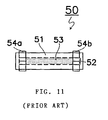
- a chip antenna generally indicated by 50 includes: a rectangular-prism-shaped insulator 51 formed by laminating insulating layers (not shown) made from insulating powder, such as alumina or steatite; a silvermade or silver-palladium-made conductor 52 formed in a coil-like shape inside the insulator 51; a magnetic member 53 made from magnetic powder, such as ferrite powder, and formed inside the insulator 51 and the coil-shaped conductor 52; and external connecting terminals 54a and 54b.
- the connecting terminals 54a and 54b are attached to the ends of a lead (not shown) of the conductor 52 and baked after the insulator 51 has been fired.
- the chip antenna 50 is thus constructed in such a manner that the coil-shaped conductor 52 is wound around the magnetic member 53, and both the elements are encapsulated by the insulator 51.
- a chip antenna comprising: a base member made from at least one of a dielectric material and a magnetic material; at least one conductor formed at least on a surface of or inside the base member; and at least one feeding terminal formed on a surface of the base member, for applying voltage to the conductor, wherein the conductor is connected at one end to the feeding terminal and at the other end to a portion of the conductor other than the end of the conductor connected to the feeding terminal.
- At least one conductor formed at least on a surface of or inside the base member is connected at one end to the feeding terminal and at the other end to a portion of the conductor other than the end of the conductor connected to the feeding terminal.
- the inductance of the conductor can be decreased, thereby enabling an increase in the resonant frequency.
- the other end of the conductor leads to a portion located midway within the conductor, and this midway portion of the conductor looks apparently greater in width.
- the radiating efficiency of the chip antenna can be enhanced, thereby increasing the band width ratio.
- a chip antenna comprising: a base member made from at least one of a dielectric material and a magnetic material; at least one conductor formed at least one of on a surface of and inside the base member; and at least one feeding terminal formed on a surface of the base member, for applying voltage to the conductor, wherein the conductor is connected at both one end and the other end to the same feeding terminal so as to be formed in a loop-like shape.
- At least one conductor formed at least one of on a surface of and inside the base member is connected at both ends to the feeding terminal so as to be formed in a loop-like shape.
- the inductance of the conductor can be made even smaller, thereby achieving an increase in the resonant frequency without needing to shorten the conductor, i.e., without lowering the gain of the chip antenna.
- one portion of the loop-like conductor may be short-circuited with another portion of the conductor.
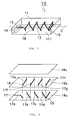
- a chip antenna generally designated by 10 includes a rectangular-prism shaped base member 11 having a mounting surface 111, and a conductor 12 formed within the base member 11.
- the conductor 12 is spirally wound in the direction of the winding axis C positioned in parallel to the mounting surface 111, i.e., in the longitudinal direction of the base member 11.
- One end of the conductor 12 is extended to a surface of the base member 11 to form a feeding section 13, which is connected to a feeding terminal 14, disposed over the surfaces of the base member 11 to apply voltage to the conductor 12.
- the other end of the conductor 12 is connected inside the base member 11 to a portion of the conductor 12 other than the feeding section 13 (which is one end of the conductor 12), for example, to a portion 15 positioned midway in the conductor 12 (hereinafter referred to as "the midway portions).
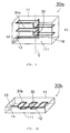
- the base member 11 is formed, as illustrated in Fig. 2, by laminating rectangular sheet layers 16a through 16c made from a dielectric material (relative dielectric constant: 6.1) comprising e.g., barium oxide, aluminum oxide and silica.
- a dielectric material relative dielectric constant: 6.1
- Formed on the surfaces of the sheet layers 16b and 16c are copper-made or copper-alloy-made conductive patterns 17a through 17h formed generally in an "L" shape or in a linear shape by means such as printing, vapor deposition, cladding, or plating.
- via-holes 18 are provided in predetermined positions (both ends of the individual conductive patterns 17e through 17h) in the sheet layer 16b in the thickness direction.
- the sheet layers 16a through 16c are laminated and sintered, and the conductive patterns 17a through 17h are connected by via holes 18.
- the above-described spirally-wound conductor 12 having a rectangular cross section can be formed in which one end of the conductor 12 serves as the feeding section 13 and the other end is connected to the midway portion 15 of the conductor 12.
- Fig. 3 is a perspective view of an example of modifications of the first embodiment.
- the chip antenna 10a differs from the chip antenna 10 of the first embodiment in that a conductor 12a is spirally wound in the direction of the winding axis C of the conductor 12a which winding axis is orthogonal to the mounting surface 111, i.e. in the direction along the height of the base member 11.
- the conductor end loops back and connects to a midway portion at point 15.
- Fig. 4 is a perspective view of another example of modifications of the first embodiment.
- the chip antenna 10b is different from the chip antenna 10 of the first embodiment in that a conductor 12b is formed in a meandering shape.
- the conductor end loops back and connects to a midway portion at point 15.
- the chip antenna of the first embodiment is constructed such that the spirally-formed or meanderingly-shaped conductor is connected at one end to the feeding terminal and at the other end to a midway portion of the conductor, the inductance of the conductor can be decreased, thereby increasing the resonant frequency. Additionally, the end of the conductor is connected to its midway portion so as to form a loop-like shape, and thus, such a loop-like portion looks apparently larger in width. Accordingly, the radiating efficiency of the chip antenna can be improved, thereby enabling an increased bandwidth ratio.
- Fig. 5 is a perspective view of a chip antenna according to a second embodiment of the present invention.
- the chip antenna generally represented by 20 differs from the chip antenna 10 of the previous embodiment in the following point.
- Both ends of a conductor 21 disposed within the base member 11 are connected to the feeding terminal 14 which is formed over the surfaces of the base member 11 to apply voltage to the conductor 21.
- the conductor 21 is thus wholly formed in a loop-like shape.
- the chip antenna 20a differs from the chip antenna 20 of the second embodiment in that a conductor 21a is spirally wound in the direction of the winding axis C of the conductor 21a which winding axis is orthogonal to the mounting surface 111, i.e. in the direction along the height of the base member 11.
- Fig. 7 is a perspective view of another example of modifications of the second embodiment.
- the chip antenna 20b is different from the chip antenna 20 of the second embodiment in that a conductor 21b is formed in a meandering shape.
- the chip antenna of the second embodiment is constructed in such a manner that the spirally-formed or meanderingly-shaped conductor is connected at both ends to the feeding terminal to form a wholly loop-like shape, so that the inductance of the conductor can be made even smaller as compared with the first embodiment. Accordingly, the resonant frequency can be increased to a greater level without needing to decrease the length of the conductor, i.e., without lowering the gain of the antenna.
- a chip antenna of a third embodiment of the present invention is shown in Fig. 8.
- the chip antenna generally indicated by 30 is different from the chip antenna 20 of the second embodiment in that one portion of a loop-like conductor 31 is short-circuited with another portion of the conductor 31 through a conductor 32.
- the chip antenna 30a differs from the chip antenna 30 of this embodiment in that a conductor 31a is spirally wound in the direction of the winding axis C of the conductor 31a which winding axis is orthogonal to the mounting surface 111, i.e. in the direction along the height of the base member 11.
- Fig. 10 is a perspective view of another example of modifications of the third embodiment.
- the chip antenna 30b is different from the chip antenna 30 of this embodiment in that a conductor 31b is formed in a meandering shape.
- the chip antenna of the third embodiment is constructed in such a manner that one portion of the spirally-formed or meanderingly-shaped conductor in a loop-like shape is short-circuited with another portion of the conductor.
- the inductance of the conductor can be made even smaller as compared with the first and second embodiments.
- the resonant frequency can be increased without changing the overall length of the conductor.
- the base member is made from a dielectric material preferably comprising barium oxide, aluminum oxide and silica.
- the base member may be made from a dielectric material comprising titanium oxide and neodymium oxide, a magnetic material comprising nickel, cobalt and iron, or a combination of a dielectric material and a magnetic material.
- the base member is rectangular-prism shaped, it may be formed in other shapes providing a mounting surface, such as a cube, cylinder, pyramid, cone, or sphere.
- the conductors shown are formed within the base member, but it may be disposed on the surface of the base member, or may be formed both on the surface of and inside the base member. Only one conductor is provided in the above-described embodiments, but two or more conductors may be formed, in which case, a resulting chip antenna can possess a plurality of resonant frequencies.
- the cross-sectional shape of the spirally-wound conductor crossing at right angles with the winding axis C is generally rectangular. However, it may be formed in other shapes as long as it partially has a linear portion.
- the length of the conductor can be increased to elevate the inductance of the conductor as compared with a conductor having a circular cross section, on condition that both types of conductors have the same cross-sectional area, thereby enhancing the gain of the resulting chip antenna.
- such an antenna can be responsive to both main polarization in the direction of the winding axis and cross polarization in the direction perpendicular to the winding axis, thereby achieving a nondirectional chip antenna.
- the number of corners provided in a meanderingly-shaped conductor is not an essential condition to carry out the present invention. Any number of corners may be formed according to the length of the conductor.
- the meandering shape is generally rectangular, it may be formed generally in a wave shape or sawtooth shape.
- the position of the feeding terminal specified in the above embodiments is not essential to carry out the present invention. Further, although the loop-like conductor is connected in only one portion in the third embodiment, it may be connected in more than one portion.
Landscapes
- Details Of Aerials (AREA)
Applications Claiming Priority (2)
| Application Number | Priority Date | Filing Date | Title |
|---|---|---|---|
| JP94374/96 | 1996-04-16 | ||
| JP8094374A JPH09284029A (ja) | 1996-04-16 | 1996-04-16 | チップアンテナ |
Publications (2)
| Publication Number | Publication Date |
|---|---|
| EP0802577A1 true EP0802577A1 (fr) | 1997-10-22 |
| EP0802577B1 EP0802577B1 (fr) | 1999-03-24 |
Family
ID=14108552
Family Applications (1)
| Application Number | Title | Priority Date | Filing Date |
|---|---|---|---|
| EP97106306A Expired - Lifetime EP0802577B1 (fr) | 1996-04-16 | 1997-04-16 | Antenne pastille |
Country Status (4)
| Country | Link |
|---|---|
| US (1) | US5861852A (fr) |
| EP (1) | EP0802577B1 (fr) |
| JP (1) | JPH09284029A (fr) |
| DE (1) | DE69700152T2 (fr) |
Cited By (3)
| Publication number | Priority date | Publication date | Assignee | Title |
|---|---|---|---|---|
| EP0831546A3 (fr) * | 1996-09-20 | 1998-04-01 | Murata Manufacturing Co., Ltd. | Chip d'antenne et dispostif d'antenne |
| US6329961B1 (en) | 1996-08-22 | 2001-12-11 | Murata Manufacturing Co., Ltd. | Antenna and resonant-frequency-adjustment method therefor |
| WO2003028149A1 (fr) * | 2001-09-25 | 2003-04-03 | Matsushita Electric Industrial Co., Ltd. | Dispositif d'antenne et equipement de communication utilisant ce dispositif |
Families Citing this family (9)
| Publication number | Priority date | Publication date | Assignee | Title |
|---|---|---|---|---|
| US6222489B1 (en) * | 1995-08-07 | 2001-04-24 | Murata Manufacturing Co., Ltd. | Antenna device |
| US6023251A (en) * | 1998-06-12 | 2000-02-08 | Korea Electronics Technology Institute | Ceramic chip antenna |
| KR100275279B1 (ko) * | 1998-12-01 | 2000-12-15 | 김춘호 | 적층형 헬리컬 안테나 |
| FR2808943B1 (fr) * | 2000-05-12 | 2004-10-01 | Valeo Electronique | Identifiant pour systeme "d'acces et demarrage mains-libres" avec une bobine emettrice et/ou receptrice disposee dans l'epaisseur du substrat |
| JP4628611B2 (ja) * | 2000-10-27 | 2011-02-09 | 三菱マテリアル株式会社 | アンテナ |
| JP3774136B2 (ja) * | 2000-10-31 | 2006-05-10 | 三菱マテリアル株式会社 | アンテナ及びそれを用いた電波送受信装置 |
| EP2026406A1 (fr) * | 2007-08-14 | 2009-02-18 | Oticon A/S | Unité d'antenne multifonction |
| JP5094527B2 (ja) * | 2008-04-23 | 2012-12-12 | 京セラ株式会社 | 構造体、及びそれを用いた電池、並びに電子装置 |
| KR102565121B1 (ko) * | 2018-11-21 | 2023-08-08 | 삼성전기주식회사 | 칩 안테나 |
Citations (3)
| Publication number | Priority date | Publication date | Assignee | Title |
|---|---|---|---|---|
| US5014071A (en) * | 1989-06-30 | 1991-05-07 | Motorola, Inc. | Ferrite rod antenna |
| EP0621653A2 (fr) * | 1993-04-23 | 1994-10-26 | Murata Manufacturing Co., Ltd. | Unité d'antenne montable en surface |
| EP0687030A1 (fr) * | 1994-05-10 | 1995-12-13 | Murata Manufacturing Co., Ltd. | Unité d'antenne |
Family Cites Families (5)
| Publication number | Priority date | Publication date | Assignee | Title |
|---|---|---|---|---|
| US5764197A (en) * | 1995-06-20 | 1998-06-09 | Murata Manufacturing Co., Ltd. | Chip antenna |
| JPH0964628A (ja) * | 1995-08-23 | 1997-03-07 | Murata Mfg Co Ltd | アンテナ装置 |
| JP3289572B2 (ja) * | 1995-09-19 | 2002-06-10 | 株式会社村田製作所 | チップアンテナ |
| JPH0993021A (ja) * | 1995-09-25 | 1997-04-04 | Murata Mfg Co Ltd | チップアンテナ |
| JP3114582B2 (ja) * | 1995-09-29 | 2000-12-04 | 株式会社村田製作所 | 表面実装型アンテナおよびこれを用いた通信機 |
-
1996
- 1996-04-16 JP JP8094374A patent/JPH09284029A/ja active Pending
-
1997
- 1997-04-11 US US08/827,782 patent/US5861852A/en not_active Expired - Lifetime
- 1997-04-16 DE DE69700152T patent/DE69700152T2/de not_active Expired - Lifetime
- 1997-04-16 EP EP97106306A patent/EP0802577B1/fr not_active Expired - Lifetime
Patent Citations (3)
| Publication number | Priority date | Publication date | Assignee | Title |
|---|---|---|---|---|
| US5014071A (en) * | 1989-06-30 | 1991-05-07 | Motorola, Inc. | Ferrite rod antenna |
| EP0621653A2 (fr) * | 1993-04-23 | 1994-10-26 | Murata Manufacturing Co., Ltd. | Unité d'antenne montable en surface |
| EP0687030A1 (fr) * | 1994-05-10 | 1995-12-13 | Murata Manufacturing Co., Ltd. | Unité d'antenne |
Cited By (4)
| Publication number | Priority date | Publication date | Assignee | Title |
|---|---|---|---|---|
| US6329961B1 (en) | 1996-08-22 | 2001-12-11 | Murata Manufacturing Co., Ltd. | Antenna and resonant-frequency-adjustment method therefor |
| EP0831546A3 (fr) * | 1996-09-20 | 1998-04-01 | Murata Manufacturing Co., Ltd. | Chip d'antenne et dispostif d'antenne |
| WO2003028149A1 (fr) * | 2001-09-25 | 2003-04-03 | Matsushita Electric Industrial Co., Ltd. | Dispositif d'antenne et equipement de communication utilisant ce dispositif |
| US6900768B2 (en) | 2001-09-25 | 2005-05-31 | Matsushita Electric Industrial Co., Ltd. | Antenna device and communication equipment using the device |
Also Published As
| Publication number | Publication date |
|---|---|
| EP0802577B1 (fr) | 1999-03-24 |
| DE69700152T2 (de) | 1999-08-19 |
| US5861852A (en) | 1999-01-19 |
| DE69700152D1 (de) | 1999-04-29 |
| JPH09284029A (ja) | 1997-10-31 |
Similar Documents
| Publication | Publication Date | Title |
|---|---|---|
| KR100414765B1 (ko) | 세라믹 칩 안테나 | |
| US6064351A (en) | Chip antenna and a method for adjusting frequency of the same | |
| EP0923153B1 (fr) | Chip d'antenne | |
| US5973651A (en) | Chip antenna and antenna device | |
| US6583769B2 (en) | Chip antenna | |
| EP0743699B1 (fr) | Système d'antenne montable en surface | |
| JP3147756B2 (ja) | チップアンテナ | |
| US6819289B2 (en) | Chip antenna with parasitic elements | |
| JPH09162624A (ja) | チップアンテナ | |
| US20020067235A1 (en) | High Q spiral inductor | |
| JP2000022421A (ja) | チップアンテナ及びそれを搭載した無線機器 | |
| JPH10145123A (ja) | ミアンダラインアンテナ | |
| EP1227538A1 (fr) | Antenne | |
| US5861852A (en) | Chip antenna | |
| US6512493B2 (en) | Chip antenna | |
| US6628241B1 (en) | Antenna device and communication terminal comprising the same | |
| US5933116A (en) | Chip antenna | |
| US5999146A (en) | Antenna device | |
| US6054956A (en) | Antenna unit having power radiation conductor | |
| US6525692B2 (en) | Dual-band antenna for mobile telecommunication units | |
| US6987494B2 (en) | Antenna assemblies for wireless communication devices | |
| US5764197A (en) | Chip antenna | |
| JPH1098405A (ja) | アンテナ装置 | |
| JP3644193B2 (ja) | アンテナ装置 | |
| JPH0983238A (ja) | 多波共用アンテナ装置 |
Legal Events
| Date | Code | Title | Description |
|---|---|---|---|
| PUAI | Public reference made under article 153(3) epc to a published international application that has entered the european phase |
Free format text: ORIGINAL CODE: 0009012 |
|
| 17P | Request for examination filed |
Effective date: 19970416 |
|
| AK | Designated contracting states |
Kind code of ref document: A1 Designated state(s): DE FR GB |
|
| 17Q | First examination report despatched |
Effective date: 19971126 |
|
| GRAG | Despatch of communication of intention to grant |
Free format text: ORIGINAL CODE: EPIDOS AGRA |
|
| GRAG | Despatch of communication of intention to grant |
Free format text: ORIGINAL CODE: EPIDOS AGRA |
|
| GRAH | Despatch of communication of intention to grant a patent |
Free format text: ORIGINAL CODE: EPIDOS IGRA |
|
| GRAH | Despatch of communication of intention to grant a patent |
Free format text: ORIGINAL CODE: EPIDOS IGRA |
|
| GRAA | (expected) grant |
Free format text: ORIGINAL CODE: 0009210 |
|
| AK | Designated contracting states |
Kind code of ref document: B1 Designated state(s): DE FR GB |
|
| ET | Fr: translation filed | ||
| REF | Corresponds to: |
Ref document number: 69700152 Country of ref document: DE Date of ref document: 19990429 |
|
| PLBE | No opposition filed within time limit |
Free format text: ORIGINAL CODE: 0009261 |
|
| STAA | Information on the status of an ep patent application or granted ep patent |
Free format text: STATUS: NO OPPOSITION FILED WITHIN TIME LIMIT |
|
| 26N | No opposition filed | ||
| REG | Reference to a national code |
Ref country code: GB Ref legal event code: IF02 |
|
| REG | Reference to a national code |
Ref country code: FR Ref legal event code: PLFP Year of fee payment: 20 |
|
| PGFP | Annual fee paid to national office [announced via postgrant information from national office to epo] |
Ref country code: GB Payment date: 20160421 Year of fee payment: 20 Ref country code: DE Payment date: 20160421 Year of fee payment: 20 |
|
| PGFP | Annual fee paid to national office [announced via postgrant information from national office to epo] |
Ref country code: FR Payment date: 20160421 Year of fee payment: 20 |
|
| REG | Reference to a national code |
Ref country code: DE Ref legal event code: R071 Ref document number: 69700152 Country of ref document: DE |
|
| REG | Reference to a national code |
Ref country code: GB Ref legal event code: PE20 Expiry date: 20170415 |
|
| PG25 | Lapsed in a contracting state [announced via postgrant information from national office to epo] |
Ref country code: GB Free format text: LAPSE BECAUSE OF EXPIRATION OF PROTECTION Effective date: 20170415 |