EP0802619A1 - Vorrichtung mit gestapelten Thyristoren und Freilaufdioden - Google Patents
Vorrichtung mit gestapelten Thyristoren und Freilaufdioden Download PDFInfo
- Publication number
- EP0802619A1 EP0802619A1 EP97400840A EP97400840A EP0802619A1 EP 0802619 A1 EP0802619 A1 EP 0802619A1 EP 97400840 A EP97400840 A EP 97400840A EP 97400840 A EP97400840 A EP 97400840A EP 0802619 A1 EP0802619 A1 EP 0802619A1
- Authority
- EP
- European Patent Office
- Prior art keywords
- thyristor
- anode
- cathode
- drl
- cooling device
- Prior art date
- Legal status (The legal status is an assumption and is not a legal conclusion. Google has not performed a legal analysis and makes no representation as to the accuracy of the status listed.)
- Granted
Links
- 238000001816 cooling Methods 0.000 claims abstract description 99
- 239000004065 semiconductor Substances 0.000 claims description 25
- 230000004224 protection Effects 0.000 claims description 13
- 239000003990 capacitor Substances 0.000 claims description 6
- 230000002441 reversible effect Effects 0.000 claims description 2
- 238000010586 diagram Methods 0.000 description 6
- 230000008901 benefit Effects 0.000 description 4
- 238000004519 manufacturing process Methods 0.000 description 2
- 230000004087 circulation Effects 0.000 description 1
- 239000002826 coolant Substances 0.000 description 1
- 230000004048 modification Effects 0.000 description 1
- 238000012986 modification Methods 0.000 description 1
Images


Classifications
-
- H—ELECTRICITY
- H02—GENERATION; CONVERSION OR DISTRIBUTION OF ELECTRIC POWER
- H02M—APPARATUS FOR CONVERSION BETWEEN AC AND AC, BETWEEN AC AND DC, OR BETWEEN DC AND DC, AND FOR USE WITH MAINS OR SIMILAR POWER SUPPLY SYSTEMS; CONVERSION OF DC OR AC INPUT POWER INTO SURGE OUTPUT POWER; CONTROL OR REGULATION THEREOF
- H02M7/00—Conversion of AC power input into DC power output; Conversion of DC power input into AC power output
- H02M7/42—Conversion of DC power input into AC power output without possibility of reversal
- H02M7/44—Conversion of DC power input into AC power output without possibility of reversal by static converters
- H02M7/48—Conversion of DC power input into AC power output without possibility of reversal by static converters using discharge tubes with control electrode or semiconductor devices with control electrode
- H02M7/505—Conversion of DC power input into AC power output without possibility of reversal by static converters using discharge tubes with control electrode or semiconductor devices with control electrode using devices of a thyratron or thyristor type requiring extinguishing means
- H02M7/515—Conversion of DC power input into AC power output without possibility of reversal by static converters using discharge tubes with control electrode or semiconductor devices with control electrode using devices of a thyratron or thyristor type requiring extinguishing means using semiconductor devices only
- H02M7/519—Conversion of DC power input into AC power output without possibility of reversal by static converters using discharge tubes with control electrode or semiconductor devices with control electrode using devices of a thyratron or thyristor type requiring extinguishing means using semiconductor devices only in a push-pull configuration
-
- H—ELECTRICITY
- H02—GENERATION; CONVERSION OR DISTRIBUTION OF ELECTRIC POWER
- H02M—APPARATUS FOR CONVERSION BETWEEN AC AND AC, BETWEEN AC AND DC, OR BETWEEN DC AND DC, AND FOR USE WITH MAINS OR SIMILAR POWER SUPPLY SYSTEMS; CONVERSION OF DC OR AC INPUT POWER INTO SURGE OUTPUT POWER; CONTROL OR REGULATION THEREOF
- H02M7/00—Conversion of AC power input into DC power output; Conversion of DC power input into AC power output
- H02M7/003—Constructional details, e.g. physical layout, assembly, wiring or busbar connections
Definitions
- the present invention relates to power semiconductor devices and their electrical interface devices, in general, and relates, more particularly, to a device with stack of thyristors and freewheeling diodes.
- Power semiconductor devices are elements composed of power semiconductors that may be different from each other.
- thyristors for example, thyristors, diodes and freewheeling diodes.
- These power semiconductor elements are cooled by means of heat dissipating coolers by circulation of a coolant.
- Each of the power semiconductor elements is sandwiched between two holding elements, one of these holding elements or the two holding elements possibly being a cooling device.
- the assembly of power semiconductor elements and holding elements constitutes a single device with a stack of thyristors and freewheeling diodes.
- This thyristor and freewheeling diode stack device is also designated by the term battery.
- Power semiconductor elements must be protected electrically by means of a protection circuit, namely capacitors.
- the various electrical connections between the power semiconductor elements and the protection circuit are made at the level of each of the cooling devices or, failing this, at the level of a holding means in the absence of a cooling device.
- the holding means ensures electrical continuity between two power semiconductor elements or between a power semiconductor element and a protection circuit.
- the power semiconductor element and holding element assemblies may be different from the fact that they derive from the electrical diagram adopted.
- the electrical supply + HT, -HT and PM output connections of the thyristor stacking device GTO and free-wheeling diodes DRL and the electrical connections Cs, Cc between the diodes Ds, Dc and the protection circuit are therefore different. from one electrical diagram to another.
- an object of the invention is a device stacking thyristors and freewheeling diodes, allowing a single wiring regardless of the electrical function of the power semiconductor device.
- Another object of the invention is a device with a stack of thyristors and freewheeling diodes, requiring a minimum of cooling devices.
- the device for stacking GTO thyristors and DRL freewheeling diodes for a semiconductor device said stacking device comprising terminals for electrical connection of power supply + HT, -HT and output PM of said stacking device, said stacking device, is characterized in that the geometric arrangement of the wiring of said electrical connection terminals + HT, PM and -HT is predetermined so as to allow the arrangement of said GTO thyristors and said wheel diodes to be modified free DRL in said stack in order to obtain different electrical functions of the semiconductor device.
- An advantage of the stacking device of the invention is the use of standard electrical connection means, for example a bus bar, for electrically connecting the stacking device and the protection circuit of this device.
- Another advantage of the stacking device of the invention is the possibility of optimizing the number of cooling devices while retaining a single connection for several applications of the semiconductor device.
- Another advantage of the stacking device of the invention is the production of a line of standard products of the mixed bridge type with forced switching or of the inverter type.
- Another advantage of the stacking device of the invention is the production of standard products with high thermal power or with lower thermal power, always while retaining a single connection.
- the device for stacking thyristors GTO, freewheeling diodes DRL and diodes D of the invention is intended for semiconductor devices of the converter type.
- the stacking device has electrical connection terminals for power supply + HT, -HT and output PM.
- the stacking device is supplemented by electrical connection terminals Cs, Cc between diodes Ds, Dc and a protection circuit P.
- the stacking device is such that the geometrical arrangement of the wiring of the electrical connection terminals + HT, PM and -HT is predetermined.
- FIG. 1 shows the known electrical diagram of a converter arm of the mixed bridge type with forced switching or of the inverter type.
- each face of the thyristors requires a cooling device.
- FIGS. 2 and 3 show a schematic representation of two preferred embodiments of the stacking device for a converter and, more particularly, for a mixed bridge with forced switching.
- the stacking device 1A for a forced switching mixed bridge successively comprises a first cooling device R1, a first thyristor GTOs, a second cooling device R2, a first freewheeling diode DRLs, a third device cooling R3, a second freewheeling diode DRLi, a fourth cooling device R4, a second thyristor GTOi and a fifth cooling device R5.
- the anode of the first GTOs thyristor is connected to the potential + HT.
- the anode of the second thyristor GTOi is connected to the terminal PM.
- the cathode of the first GTOs thyristor is connected to the PM terminal.
- the cathode of the second thyristor GTOi is connected to the potential -HT.
- the anode of the first free-wheeling diode DRLs is connected to the terminal PM.
- the anode of the second freewheeling diode DRLi is connected to the potential -HT.
- the cathode of the first free-wheeling diode DRLs is connected to the potential + HT.
- the cathode of the second freewheeling diode DRLi is connected to the terminal PM.
- the + HT connection terminal is connected to the anode of the first thyristor GTOs and to the cathode of the first freewheeling diode DRLs.
- the PM connection terminal is connected to the anode of the first freewheeling diode DRLs and to the cathode of the second freewheeling diode DRLi as well as to the cathode of the first thyristor GTOs and to the anode of the second thyristor GTOi .
- connection terminal -HT is connected to the anode of the second freewheeling diode DRLi and to the cathode of the second thyristor GTOi.
- the device 1B for a mixed bridge with forced switching successively comprises a first cooling device R1, a first freewheeling diode DRLs, a second cooling device R2, a first thyristor GTOs, a third cooling device R3, a second thyristor GTOi, a fourth cooling device R4, a second freewheeling diode DRLi and a fifth cooling device R5.
- the anode of the first GTOs thyristor is connected to the potential + HT.
- the anode of the second thyristor GTOi is connected to the terminal PM.
- the cathode of the first GTOs thyristor is connected to the PM terminal.
- the cathode of the second thyristor GTOi is connected to the potential -HT.
- the anode of the first free-wheeling diode DRL's is connected to the terminal PM.
- the anode of the second freewheeling diode DRL'i is connected to the potential -HT.
- the cathode of the first free-wheeling diode DRL's is connected to the potential + HT.
- the cathode of the second freewheeling diode DRL'i is connected to the terminal PM.
- the + HT connection terminal is connected to the cathode of the first freewheeling diode DRLs and to the anode of the first thyristor GTOs.
- the PM connection terminal is connected to the cathode of the first thyristor GTOs and to the anode of the second thyristor GTOi as well as to the anode of the first freewheeling diode DRLs and to the cathode of the second freewheeling diode DRLi .
- connection terminal -HT is connected to the cathode of the second thyristor GTOi and to the anode of the second freewheeling diode DRLi.
- the third cooling devices R3 (FIG. 2) and the first R1 and fifth R5 cooling devices (FIG. 3) can be replaced by conductive elements in the case less thermal power to transmit.
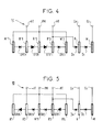
- Figures 4 and 5 show a schematic representation of two preferred embodiments of the stacking device for converter and, more particularly, for inverter.
- the stacking device 1C for inverter successively comprises a first conductive element M'1, a first free-wheeling diode DRL's, a first cooling device R'1, a first thyristor GTO's, a second cooling device R'2, a second thyristor GTO'i, a third cooling device R'3, a second freewheeling diode DRL'i and a second conductive element M'2.
- the anode of the first GTO's thyristor is connected to the potential + HT.
- the anode of the second thyristor GTO'i is connected to the terminal PM.
- the cathode of the first GTO's thyristor is connected to the PM terminal.
- the cathode of the second thyristor GTO'i is connected to the potential -HT.
- the anode of the first free-wheeling diode DRL's is connected to the terminal PM.
- the anode of the second freewheeling diode DRL'i is connected to the potential -HT.
- the cathode of the first free-wheeling diode DRL's is connected to the potential + HT.
- the cathode of the second freewheeling diode DRL'i is connected to the terminal PM.
- the + HT connection terminal is connected to the cathode of the first free-wheeling diode DRL's and to the anode of the first thyristor GTO's.
- the PM connection terminal is connected to the cathode of the first thyristor GTO's and to the anode of the second thyristor GTO'i as well as to the anode of the first free wheel diode DRL's and to the cathode of the second wheel diode free DRL'i.
- connection terminal -HT is connected to the cathode of the second thyristor GTO'i and to the anode of the second freewheeling diode DRL'i.
- the stacking device 1D for an inverter successively comprises a first cooling device R'1, a first thyristor GTO's, a second cooling device R'2, a first free-wheeling diode DRL's, a first conducting element M'1, a second free-wheeling diode DRL'i, a third cooling device R'3, a second thyristor GTO'i and a third cooling device R'5.
- the anode of the first GTO's thyristor is connected to the potential + HT.
- the anode of the second thyristor GTO'i is connected to the terminal PM.
- the cathode of the first GTO's thyristor is connected to the PM terminal.
- the cathode of the second thyristor GTO'i is connected to the potential -HT.
- the anode of the first free-wheeling diode DRL's is connected to the terminal PM.
- the anode of the second freewheeling diode DRL'i is connected to the potential -HT.
- the cathode of the first free-wheeling diode DRL's is connected to the potential + HT.
- the cathode of the second freewheeling diode DRL'i is connected to the terminal PM.
- the + HT connection terminal is connected to the anode of the first thyristor GTO's and to the cathode of the first free-wheeling diode DRL's.
- the PM connection terminal is connected to the anode of the first free-wheeling diode DRL's and to the cathode of the second free-wheeling diode DRL'i as well as to the cathode of the first thyristor GTO's and to the anode of the second thyristor GTO'i.
- connection terminal -HT is connected to the anode of the second freewheeling diode DRL'i and to the cathode of the second thyristor GTO'i.
- FIG. 6 shows the known electrical diagram of a converter arm of the chopper type.
- Figures 7 and 8 show a schematic representation of two preferred embodiments of the stacking device for converter and, more particularly, for chopper.
- the stacking device 1E for chopper successively comprises a first conducting element M "1, a first free-wheeling diode DRL” s, a first cooling device R “1, a thyristor GTO” s, a second cooling device R “2, a second freewheeling diode DRL” i, a third cooling device R “3, an insulating element I” and a second conducting element M "2.
- the anode of thyristor GTO "s is connected to the potential + HT.
- the cathode of thyristor GTO "s is connected to terminal PM.
- the anode of the first free-wheeling diode DRL "s is connected to the terminal PM.
- the anode of the second freewheeling diode DRL "i is connected to the potential -HT.
- the cathode of the first free-wheeling diode DRL "s is connected to the potential + HT.
- the cathode of the second freewheeling diode DRL "i is connected to the terminal PM.
- connection terminal + HT is connected to the cathode of the first free-wheeling diode DRL "s and to the anode of the thyristor GTO" s.
- the PM connection terminal is connected to the thyristor cathode GTO "s and to the cathode of the second freewheeling diode DRL" i as well as to the anode of the first freewheeling diode DRL "s.
- connection terminal -HT is connected to the anode of the second freewheeling diode DRL "i.
- the stacking device 1F for chopper successively comprises a first conductive element M "1, a first wheel diode free DRL “s, a first cooling device R” 1, a thyristor GTO “s, a second cooling device R” 2, an insulating element I “, a third cooling device R” 3, a second freewheeling diode DRL “i and a fourth cooling device R" 4.
- the thyristor GTO "s and the insulating element I" are in series.
- the anode of thyristor GTO "s is connected to the potential + HT.
- the cathode of thyristor GTO "s is connected to terminal PM.
- the anode of the first free-wheeling diode DRL "s is connected to the terminal PM.
- the anode of the second freewheeling diode DRL "i is connected to the potential -HT.
- the cathode of the first free-wheeling diode DRL "s is connected to the potential + HT.
- the cathode of the second freewheeling diode DRL "i is connected to the terminal PM.
- connection terminal + HT is connected to the cathode of the first free-wheeling diode DRL "s and to the anode of the thyristor GTO" s.
- the PM connection terminal is connected to the thyristor cathode GTO "s as well as to the anode of the first free-wheeling diode DRL" s and to the cathode of the second free-wheeling diode DRL "i.
- connection terminal -HT is connected to the anode of the second freewheeling diode DRL "i.
- the stacking device 1A-1F of the invention is successively supplemented by a first diode Ds, a cooling device R, a second diode Dc and a conductive element M.
- the cathode of the first diode Ds is connected to the potential -HT.
- the anode of the first diode Ds and the cathode of the second diode Dc are connected to the terminal Cs.
- the anode of the second diode Dc is connected to the terminal Cc.
- a capacitor Cs of the protection circuit P is disposed between the electrical output connection terminal PM and the common terminal Cs of the first Ds and second diode Dc.
- the third cooling devices R “3 (FIG. 7) and the third R" 3 or fourth R “4 cooling devices (FIG. 8) can be replaced by conductive elements in the case of a lower thermal power to be transmitted.
Landscapes
- Engineering & Computer Science (AREA)
- Power Engineering (AREA)
- Inverter Devices (AREA)
- Rectifiers (AREA)
- Power Conversion In General (AREA)
Applications Claiming Priority (2)
| Application Number | Priority Date | Filing Date | Title |
|---|---|---|---|
| FR9604870 | 1996-04-18 | ||
| FR9604870A FR2747857B1 (fr) | 1996-04-18 | 1996-04-18 | Dispositif a empilement de thyristors et de diodes de roue libre |
Publications (2)
| Publication Number | Publication Date |
|---|---|
| EP0802619A1 true EP0802619A1 (de) | 1997-10-22 |
| EP0802619B1 EP0802619B1 (de) | 2001-12-05 |
Family
ID=9491341
Family Applications (1)
| Application Number | Title | Priority Date | Filing Date |
|---|---|---|---|
| EP97400840A Expired - Lifetime EP0802619B1 (de) | 1996-04-18 | 1997-04-14 | Vorrichtung mit gestapelten Thyristoren und Freilaufdioden |
Country Status (5)
| Country | Link |
|---|---|
| US (1) | US5898582A (de) |
| EP (1) | EP0802619B1 (de) |
| DE (1) | DE69708741T2 (de) |
| ES (1) | ES2167690T3 (de) |
| FR (1) | FR2747857B1 (de) |
Cited By (1)
| Publication number | Priority date | Publication date | Assignee | Title |
|---|---|---|---|---|
| WO2008003555A1 (de) * | 2006-07-07 | 2008-01-10 | Abb Research Ltd | Schaltungsanordnung zur elektrischen leistungssteuerung und kühlungsanordnung |
Families Citing this family (2)
| Publication number | Priority date | Publication date | Assignee | Title |
|---|---|---|---|---|
| EP1178593A1 (de) * | 2000-08-02 | 2002-02-06 | ABB Industrie AG | Halbleiter-Spannstapelsatz |
| US10230260B2 (en) | 2015-09-23 | 2019-03-12 | Abb Schweiz Ag | Fast utility disconnect switch for single conversion UPS |
Citations (3)
| Publication number | Priority date | Publication date | Assignee | Title |
|---|---|---|---|---|
| GB2094547A (en) * | 1981-03-09 | 1982-09-15 | Aei Semiconductor Ltd | Stack mounted electrical components |
| EP0069971A1 (de) * | 1981-07-10 | 1983-01-19 | Hitachi, Ltd. | Stapel mit GTO-Thyristoren |
| US4864385A (en) * | 1987-12-29 | 1989-09-05 | Hitachi, Ltd. | Power semiconductors connected antiparallel via heatsinks |
Family Cites Families (8)
| Publication number | Priority date | Publication date | Assignee | Title |
|---|---|---|---|---|
| US4338652A (en) * | 1980-02-26 | 1982-07-06 | Westinghouse Electric Corp. | Stack module and stack loader therefor |
| IT8167940A0 (it) * | 1981-07-06 | 1981-07-06 | Ferrero Guilio Spa | Volante di sicurezza per autoveicoli |
| DE3577787D1 (de) * | 1984-11-28 | 1990-06-21 | Bbc Brown Boveri & Cie | Induktionsarme anoden-kathodenbeschaltung eines abschaltbaren leistungsthyristors. |
| US4868712A (en) * | 1987-02-04 | 1989-09-19 | Woodman John K | Three dimensional integrated circuit package |
| US5204804A (en) * | 1992-01-15 | 1993-04-20 | General Electric Company | GTO module with piggyback bypass diode |
| US5270913A (en) * | 1992-04-06 | 1993-12-14 | D.C. Transformation, Inc. | Compact and efficient transformerless power conversion system |
| JP3153408B2 (ja) * | 1994-03-10 | 2001-04-09 | 株式会社日立製作所 | 直列多重電力変換器 |
| JP2735497B2 (ja) * | 1995-01-31 | 1998-04-02 | 株式会社東芝 | スナバ回路 |
-
1996
- 1996-04-18 FR FR9604870A patent/FR2747857B1/fr not_active Expired - Fee Related
-
1997
- 1997-04-14 EP EP97400840A patent/EP0802619B1/de not_active Expired - Lifetime
- 1997-04-14 DE DE69708741T patent/DE69708741T2/de not_active Expired - Fee Related
- 1997-04-14 ES ES97400840T patent/ES2167690T3/es not_active Expired - Lifetime
- 1997-04-17 US US08/837,394 patent/US5898582A/en not_active Expired - Lifetime
Patent Citations (3)
| Publication number | Priority date | Publication date | Assignee | Title |
|---|---|---|---|---|
| GB2094547A (en) * | 1981-03-09 | 1982-09-15 | Aei Semiconductor Ltd | Stack mounted electrical components |
| EP0069971A1 (de) * | 1981-07-10 | 1983-01-19 | Hitachi, Ltd. | Stapel mit GTO-Thyristoren |
| US4864385A (en) * | 1987-12-29 | 1989-09-05 | Hitachi, Ltd. | Power semiconductors connected antiparallel via heatsinks |
Cited By (3)
| Publication number | Priority date | Publication date | Assignee | Title |
|---|---|---|---|---|
| WO2008003555A1 (de) * | 2006-07-07 | 2008-01-10 | Abb Research Ltd | Schaltungsanordnung zur elektrischen leistungssteuerung und kühlungsanordnung |
| RU2413968C2 (ru) * | 2006-07-07 | 2011-03-10 | Абб Рисерч Лтд | Схема электрического регулирования по мощности и схема охлаждения |
| US7911755B2 (en) | 2006-07-07 | 2011-03-22 | Abb Research Ltd | Circuit arrangement for electrically controlling power and cooling arrangement |
Also Published As
| Publication number | Publication date |
|---|---|
| US5898582A (en) | 1999-04-27 |
| DE69708741D1 (de) | 2002-01-17 |
| DE69708741T2 (de) | 2002-09-26 |
| EP0802619B1 (de) | 2001-12-05 |
| ES2167690T3 (es) | 2002-05-16 |
| FR2747857B1 (fr) | 1998-05-22 |
| FR2747857A1 (fr) | 1997-10-24 |
Similar Documents
| Publication | Publication Date | Title |
|---|---|---|
| US4492975A (en) | Gate turn-off thyristor stack | |
| US4513168A (en) | Three-terminal solar cell circuit | |
| US20050128706A1 (en) | Power module with heat exchange | |
| US20150357680A1 (en) | Device and Method for Bridging an Electrical Energy Storage | |
| JPS59165471A (ja) | 太陽電池モジユ−ル | |
| FR2803702A1 (fr) | Ensemble de conversion de puissance electrique | |
| EP1590869A2 (de) | Elektrischer stromwandler für brennstoffzelle | |
| CN116584030A (zh) | 可扩展功率逆变器 | |
| FR3088137A1 (fr) | Systeme electronique de puissance | |
| FR2687009A1 (fr) | Composant de protection pour circuit automobile. | |
| EP0802619B1 (de) | Vorrichtung mit gestapelten Thyristoren und Freilaufdioden | |
| EP3646681A1 (de) | Spannungswandler, verfahren zur herstellung solch eines spannungswandlers und anordnung eines hauptmoduls und eines anschlussblockmoduls zur ausbildung solch eines spannungswandlers | |
| US4456782A (en) | Solar cell device | |
| EP3484039A1 (de) | Schaltmodul für spannungswechsel- oder gleichrichter | |
| EP0944163A1 (de) | Struktur zur industriellen Realisierung eines Mehrpegelumrichters | |
| EP0619637B1 (de) | Schutz eines Kraftfahrzeugdrehstromgenerators | |
| FR2908945A1 (fr) | Element de pont redresseur synchrone, pont redresseur synchrone correspondant et utilisation. | |
| WO2019166721A1 (fr) | Ensemble de bus barres formant boîtier et dissipateur thermique pour un dispositif électronique de puissance | |
| CA2280987C (fr) | Dispositif perfectionne d'alimentation en courant electrique de moteurs de traction de vehicules urbains ou suburbains | |
| JPS61196583A (ja) | 光起電力装置 | |
| JP2013197464A (ja) | 太陽電池回路 | |
| FR2748888A1 (fr) | Dispositif a elements semi-conducteurs de puissance | |
| FR2814907A1 (fr) | Module electronique de puissance et bras d'onduleur comportant un tel module | |
| FR2742941A1 (fr) | Dispositif electronique de puissance et dispositif d'alimentation de moteur | |
| FR3157724A1 (fr) | Sous-module d’un bras d’un convertisseur HVDC de type MMC, et convertisseur MMC comprenant un tel module |
Legal Events
| Date | Code | Title | Description |
|---|---|---|---|
| PUAI | Public reference made under article 153(3) epc to a published international application that has entered the european phase |
Free format text: ORIGINAL CODE: 0009012 |
|
| AK | Designated contracting states |
Kind code of ref document: A1 Designated state(s): BE CH DE ES GB IT LI SE |
|
| 17P | Request for examination filed |
Effective date: 19980127 |
|
| 17Q | First examination report despatched |
Effective date: 19990331 |
|
| GRAG | Despatch of communication of intention to grant |
Free format text: ORIGINAL CODE: EPIDOS AGRA |
|
| GRAG | Despatch of communication of intention to grant |
Free format text: ORIGINAL CODE: EPIDOS AGRA |
|
| GRAH | Despatch of communication of intention to grant a patent |
Free format text: ORIGINAL CODE: EPIDOS IGRA |
|
| GRAH | Despatch of communication of intention to grant a patent |
Free format text: ORIGINAL CODE: EPIDOS IGRA |
|
| GRAA | (expected) grant |
Free format text: ORIGINAL CODE: 0009210 |
|
| AK | Designated contracting states |
Kind code of ref document: B1 Designated state(s): BE CH DE ES GB IT LI SE |
|
| REG | Reference to a national code |
Ref country code: CH Ref legal event code: EP |
|
| REG | Reference to a national code |
Ref country code: CH Ref legal event code: NV Representative=s name: CABINET ROLAND NITHARDT CONSEILS EN PROPRIETE INDU |
|
| REG | Reference to a national code |
Ref country code: GB Ref legal event code: IF02 |
|
| GBT | Gb: translation of ep patent filed (gb section 77(6)(a)/1977) |
Effective date: 20011206 |
|
| REF | Corresponds to: |
Ref document number: 69708741 Country of ref document: DE Date of ref document: 20020117 |
|
| REG | Reference to a national code |
Ref country code: ES Ref legal event code: FG2A Ref document number: 2167690 Country of ref document: ES Kind code of ref document: T3 |
|
| PLBE | No opposition filed within time limit |
Free format text: ORIGINAL CODE: 0009261 |
|
| STAA | Information on the status of an ep patent application or granted ep patent |
Free format text: STATUS: NO OPPOSITION FILED WITHIN TIME LIMIT |
|
| 26N | No opposition filed | ||
| PGFP | Annual fee paid to national office [announced via postgrant information from national office to epo] |
Ref country code: ES Payment date: 20090422 Year of fee payment: 13 |
|
| PGFP | Annual fee paid to national office [announced via postgrant information from national office to epo] |
Ref country code: SE Payment date: 20090416 Year of fee payment: 13 Ref country code: IT Payment date: 20090428 Year of fee payment: 13 Ref country code: DE Payment date: 20090422 Year of fee payment: 13 |
|
| PGFP | Annual fee paid to national office [announced via postgrant information from national office to epo] |
Ref country code: BE Payment date: 20090528 Year of fee payment: 13 |
|
| PGFP | Annual fee paid to national office [announced via postgrant information from national office to epo] |
Ref country code: CH Payment date: 20090417 Year of fee payment: 13 |
|
| PGFP | Annual fee paid to national office [announced via postgrant information from national office to epo] |
Ref country code: GB Payment date: 20090421 Year of fee payment: 13 |
|
| BERE | Be: lapsed |
Owner name: S.A. *GEC ALSTHOM TRANSPORT Effective date: 20100430 |
|
| EUG | Se: european patent has lapsed | ||
| REG | Reference to a national code |
Ref country code: CH Ref legal event code: PL |
|
| GBPC | Gb: european patent ceased through non-payment of renewal fee |
Effective date: 20100414 |
|
| PG25 | Lapsed in a contracting state [announced via postgrant information from national office to epo] |
Ref country code: LI Free format text: LAPSE BECAUSE OF NON-PAYMENT OF DUE FEES Effective date: 20100430 Ref country code: DE Free format text: LAPSE BECAUSE OF NON-PAYMENT OF DUE FEES Effective date: 20101103 Ref country code: CH Free format text: LAPSE BECAUSE OF NON-PAYMENT OF DUE FEES Effective date: 20100430 |
|
| PG25 | Lapsed in a contracting state [announced via postgrant information from national office to epo] |
Ref country code: BE Free format text: LAPSE BECAUSE OF NON-PAYMENT OF DUE FEES Effective date: 20100430 Ref country code: GB Free format text: LAPSE BECAUSE OF NON-PAYMENT OF DUE FEES Effective date: 20100414 Ref country code: IT Free format text: LAPSE BECAUSE OF NON-PAYMENT OF DUE FEES Effective date: 20100414 |
|
| REG | Reference to a national code |
Ref country code: ES Ref legal event code: FD2A Effective date: 20110715 |
|
| PG25 | Lapsed in a contracting state [announced via postgrant information from national office to epo] |
Ref country code: ES Free format text: LAPSE BECAUSE OF NON-PAYMENT OF DUE FEES Effective date: 20110705 |
|
| PG25 | Lapsed in a contracting state [announced via postgrant information from national office to epo] |
Ref country code: ES Free format text: LAPSE BECAUSE OF NON-PAYMENT OF DUE FEES Effective date: 20100415 |
|
| PG25 | Lapsed in a contracting state [announced via postgrant information from national office to epo] |
Ref country code: SE Free format text: LAPSE BECAUSE OF NON-PAYMENT OF DUE FEES Effective date: 20100415 |