EP0802686B1 - Système de traitement de signal - Google Patents
Système de traitement de signal Download PDFInfo
- Publication number
- EP0802686B1 EP0802686B1 EP97302643A EP97302643A EP0802686B1 EP 0802686 B1 EP0802686 B1 EP 0802686B1 EP 97302643 A EP97302643 A EP 97302643A EP 97302643 A EP97302643 A EP 97302643A EP 0802686 B1 EP0802686 B1 EP 0802686B1
- Authority
- EP
- European Patent Office
- Prior art keywords
- signal
- value
- data point
- processing system
- signals
- Prior art date
- Legal status (The legal status is an assumption and is not a legal conclusion. Google has not performed a legal analysis and makes no representation as to the accuracy of the status listed.)
- Expired - Lifetime
Links
- 238000012935 Averaging Methods 0.000 claims 1
- 230000000694 effects Effects 0.000 description 6
- 239000000872 buffer Substances 0.000 description 5
- 239000003086 colorant Substances 0.000 description 4
- 230000015556 catabolic process Effects 0.000 description 2
- 238000006731 degradation reaction Methods 0.000 description 2
- 238000005070 sampling Methods 0.000 description 2
- 230000003068 static effect Effects 0.000 description 2
- 230000007704 transition Effects 0.000 description 2
- 241001422033 Thestylus Species 0.000 description 1
- 230000008859 change Effects 0.000 description 1
- 238000010586 diagram Methods 0.000 description 1
- 238000004519 manufacturing process Methods 0.000 description 1
- 230000004048 modification Effects 0.000 description 1
- 238000012986 modification Methods 0.000 description 1
- 238000010422 painting Methods 0.000 description 1
- 230000009467 reduction Effects 0.000 description 1
- 230000004044 response Effects 0.000 description 1
Images


Classifications
-
- H—ELECTRICITY
- H04—ELECTRIC COMMUNICATION TECHNIQUE
- H04N—PICTORIAL COMMUNICATION, e.g. TELEVISION
- H04N9/00—Details of colour television systems
- H04N9/77—Circuits for processing the brightness signal and the chrominance signal relative to each other, e.g. adjusting the phase of the brightness signal relative to the colour signal, correcting differential gain or differential phase
-
- H—ELECTRICITY
- H04—ELECTRIC COMMUNICATION TECHNIQUE
- H04N—PICTORIAL COMMUNICATION, e.g. TELEVISION
- H04N9/00—Details of colour television systems
- H04N9/64—Circuits for processing colour signals
- H04N9/646—Circuits for processing colour signals for image enhancement, e.g. vertical detail restoration, cross-colour elimination, contour correction, chrominance trapping filters
Definitions
- the invention relates to a signal processing system. More specifically the invention relates to a signal processing system for processing a pair of signals carrying related information with one of the signals having a larger bandwidth and the other of the signals having a smaller bandwidth.
- Images can be represented in an electrical environment by signals that define such image attributes as the intensity and colour of elements of the images.
- television pictures were represented by analog signals defining the luminance (Y) and the colour difference (R-Y) and (B-Y), ie chrominance, of the picture elements.
- More recently digital signals have been used to represent television pictures. Digital signals are highly resistant to degradation and can be readily processed to create special effects in the television picture.
- a component signal is used consisting of luminance (Y) and chrominance (U, V) signals that are sampled at a ratio of 4:2:2.
- the luminance signal is sampled at a rate of 13.5 MHz and the two chrominance signals are each sampled at a rate of 6.75 MHz. That is to say, the digital luminance signal has a bandwidth of 13.5 MHz and the digital chrominance signals each have a bandwidth of 6.75 MHz.
- the bandwidth is a measure of the detail in the picture. Sampling in the 4:2:2 ratio means that the horizontal resolution of the colour in the television picture is halved, but because it is the luminance that contains the picture detail this reduction in horizontal colour resolution is an acceptable compromise that enables the data rate to be reduced.
- Figure 1 of the accompanying drawings illustrates a simple picture 1 comprising two areas of different colours 2, 3, say yellow and black, with an abrupt transition 4 between the two areas.
- Figure 2 of the accompanying drawings shows a signal 5 of infinite bandwidth representing a line 6 in the picture 1.
- the infinite bandwidth of the signal 5 means that signal can represent exactly the transition 4 between the two areas 2, 3.
- the luminance (Y) and chrominance (U, V) signals would represent the line 6 in this manner. However, this does not happen in practice because of the limited bandwidth of the signals.
- Figure 3 of the accompanying drawings shows a luminance signal 7 comprising multiple sample values at evenly spaced intervals.
- the effect of limiting the bandwidth in the signal 7 is to produce a transitional zone 9 in the signal extending to each side of the boundary 4 in the picture.
- Figure 4 of the accompanying drawings shows a signal 10 having half the bandwidth of the signal 7 and corresponding to one of the chrominance signals (U or B).
- the effect of halving the bandwidth of the signal 10 as compared to that of the signal 7 is to halve the number of sampling points 11 that comprise the signal 10 and to increase the size of the transitional zone 12 on each side of the boundary 4 in the picture.
- the boundary 4 between the two areas 2, 3 will not be seen as a sharp line but will instead be seen as a blurred region that may contain unwanted colours between yellow and black. In some situations, especially when the image is static as opposed to part of a video sequence, this blurring of the boundary 4 is unacceptable.
- JP 60-201790 describes a static image camera that interpolates a chrominance signal according to the rate of change of a luminance signal to reduce the occurrence of pseudo colours.
- interpolation requires complex processing and is undesirable, particularly for moving images.
- the invention aims to minimise the above problems.
- an image processing system 20 comprising a format converter 21 for receiving signals from an external source (not shown) and supplying signals to a store 22.
- the format converter 21 is provided to enable incoming signals to be supplied in any convenient format, eg RGB, CMYK, etc., and converted into a YUV format suitable for processing by the system. Format converters are per se well known and there is therefore no need to describe the format converter 21 in any further detail herein.
- the store 22 comprises two parts 22a, 22b respectively for storing data representing the luminance (Y) and chrominance (U, V) components of the data from the format convertor.
- the data in the store represents a multiplicity of pixels which together form a picture.
- each pixel (pixel 0, pixel 1, pixel 2, etc.) has luminance data (Y 0 , Y 1 , Y 2 , etc.) associated with it. Every other pixel (pixel 0, pixel 2, pixel 4, etc.) has chrominance data (U 0 , V 0 , U 2 , V 2 , U 4 , V 4 , etc.) associated with it.
- the chrominance data is shared between two pixels (e.g. pixel 0 and pixel 1) as already described herein above.
- the system 20 further comprises a processor 23.
- the processor 23 is arranged to operate in the manner described in US Patent 4514818 and corresponding British Patent 2089625 and the system therefore includes a stylus and touch tablet device 24 to which the processor 23 is responsive.
- the YUV data in the store 22 is in a format suitable for processing by the processor 23 as described in the above mentioned patents.
- the processor 23 is arranged to respond to user manipulation of the stylus and touch tablet device to read data from the store 22, modify the data and write the modified data back to the store 22 replacing the data originally stored therein. In this way, retouching of an image by electronic "painting” or “drawing” can be effected.
- the system 20 further comprises a deriving circuit 25 connected to receive YUV data either directly from the store 22 or from the processor 23.
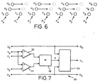
- the deriving circuit 25 is arranged to derive additional information for the UV signals from the corresponding Y signals so as to provide separate UV data for each pixel in the picture. That is to say, as shown in Figure 6, the deriving circuit 25 serves to derive UV data for pixel 1, pixel 3, pixel 5 etc. Data output from the deriving circuit 25 is received by another format converter 26 which converts the data into a desired format.
- the format converter 26 may be arranged to convert the data into an RGB format for display of the image on a monitor 27, or it may be arranged to convert the data into a CMYK format for printing of the image by a printer 28.
- the converter 26 is not limited to converting into RGB or CMYK formats, and may for example be arranged to convert the data into the so-called D2 format for storage in a bulk store device such as a video tape recorder (VTR).
- VTR video tape recorder
- FIG. 7 of the accompanying drawings shows the deriving circuit 25 in greater detail.
- the deriving circuit comprises two subtractors 30, 31 connected to receive luminance values Y 0 , Y 1 and Y 2 for three adjacent pixels.
- the subtractor 30 is arranged to calculate the magnitude of the difference between Y 0 and Y 1 , i.e.
- the subtractor 32 is arranged to calculate
- the values from the subtractors 30, 31 are input to a divider circuit which calculates a value K as the ratio of
- the value output from the divider 32 is a constant value K, and it will be noted that the constant value K is calculated purely from the luminance values of consecutive pixels Y 0 to Y 2 .
- the constant value K is input to a selecting circuit 33 together with chrominance values U 0 and U 2 for the zeroth pixel and the second pixel in the sequence of three adjacent pixels.
- the selector circuit 33 calculates from U 0 , U 2 and K a value for use as the missing value for pixel 1, i.e. the selector calculates the value for U 1 .
- the selector 33 comprises a first comparator 39 which compares the value K with a predetermined value X and outputs a signal if K is less than X.
- the selector 33 further comprises a second comparator 40 which compares the constant value K with a predetermined value Y and outputs a signal if K is greater than Y.
- the signals output from the comparators 39, 40 are applied to inverting inputs of an AND circuit 41 which therefore outputs a signal if X ⁇ K ⁇ Y.
- the chrominance signals U 0 and U 2 are input to a pair of shift registers 42, 43 and to respective tristate buffers 44, 45.
- the shift registers also receive the output from the AND circuit 41.
- the shift registers 42, 43 shift the digital values U 0 , U 2 one place to the left, that is the shift registers divide both the digital value U 0 and the digital value U 2 by two.
- the chrominance data output from the two shift registers is added together by an adder 46 which outputs a value equal to 1 ⁇ 2 U 0 + 1 ⁇ 2 U 2 .
- the output from the adder 46 is applied to a tristate buffer 47.
- the outputs from the tristate buffers 44, 45 and 47 are connected together at line 48.
- the tristate buffer 44 is driven by the output from the first comparator 39 and the tristate buffer 45 is driven by the output from the second comparator 40.
- the value U 1 output on line 48 is U 0 if K is less than X, is U 2 if K is greater than Y and is 1 ⁇ 2 U 0 + 1 ⁇ 2 U 2 if X ⁇ K ⁇ Y.
- Figure 10 shows how the luminance (Y) signal changes with distance (x) along a line in a picture.
- the luminance signal comprises plural samples 51 to 55 at equally spaced intervals along the line.
- the chrominance signal likewise comprises a plurality of evenly spaced samples 56 to 58, but the spacing between samples is twice that in the luminance signal. If one were simply to take as the unknown chrominance value the average between two known values one would develop a signal represented by the broken line 59 in Figure 11.
- the broken line 59 comprises unknown chrominance samples 60, 61 which are taken to lie on a straight line between adjacent samples 56, 57 and 57, 58.
- the true values of the unknown samples is represented by points 62 and 63 and it should be noted that there is a considerable difference between the true value 62 and the calculated average value 60 and between the true value 63 and the calculated average value 61.
- the form of the luminance signal in Figure 10 is similar (albeit not identical) to that of the chrominance signal in Figure 11.
- the deriving circuit derives unknown pixel values using a constant calculated from the slope of the luminance signal. The effect of the calculation is therefore to produce unknown chrominance values such that the slope of the chrominance signal about the unknown chrominance value tends to follow the slope of the luminance signal at the corresponding point.
- Figures 12 and 13 of the accompanying drawings show a special case where an unknown chrominance value is at a position corresponding to a peak in the luminance signal.
- the deriving circuit 25 is reconfigured to the arrangement shown in Figure 14 of the accompanying drawings.
- Difference values between Y 1 and Y 0 and between Y 1 and Y 2 are calculated by way of subtractors 70, 71.
- the value K is input to a subtractor 73 which calculates the inverse value (1 - K).
- the values K and (1 - K) are applied to respective multipliers 74, 75 together with values for U 0 and U 2 .
- the signals output from the multiplier 74, 75 are added together by way of an adder 76 whose output corresponds to the value for U 1 .
- the effect of setting K either to 0 or to 1 is to cause the deriving circuit shown in Figure 14 to select either the value U 0 or the value U 2 as the value for U 1 .
Landscapes
- Engineering & Computer Science (AREA)
- Multimedia (AREA)
- Signal Processing (AREA)
- Processing Of Color Television Signals (AREA)
- Color Television Systems (AREA)
- Image Processing (AREA)
- Apparatus For Radiation Diagnosis (AREA)
Claims (7)
- Système de traitement de signal (20) pour traiter une paire de signaux portant des informations associées, l'un des signaux ayant une plus grande largeur de bande et l'autre des signaux ayant une plus petite largeur de bande, dans lequel chacun des signaux représente les informations sous la forme d'une séquence de points de données discrets (Y0, Y1, Y2, ..., U0, U2, ...), et une valeur d'un point de données inconnu (U1) à un instant où le signal de plus petite largeur de bande est déterminé en se référant à des valeurs de points de données connus (Y0, Y1, Y2) dans le signal de plus grande largeur de bande dans une période de temps encadrant l'instant du point de données inconnu (U1) dans le signal de plus petite largeur de bande, et en se référant à des valeurs de points de données connus (U0, U2) dans le signal de plus petite largeur de bande ; caractérisé en ce que, si une différence normalisée (K) entre les points de données connus (Y0, Y1, Y2), précédant l'instant du point de données inconnu (U1), est inférieure à une première valeur prédéterminée (X), la valeur du point de données inconnu (U1) est choisie comme étant celle du point de données connu (U0) qui précède le point de données inconnu (U1) dans le signal de plus petite largeur de bande ; si la différence normalisée (K) est plus grande qu'une seconde valeur prédéterminée (Y) plus grande que la première valeur prédéterminée (X), la valeur du point de données inconnu (U1) est choisie comme étant celle du point de données connu (U2) qui fait suite au point de données inconnu (U1) dans le signal de plus petite largeur de bande ; et si la différence normalisée (K) est plus grande que la première valeur prédéterminée (X) et plus petite que la seconde valeur prédéterminée (Y), la valeur du point de données inconnu (U1) est déterminée en moyennant les valeurs du point de données précédent (U0) et du point de données suivant (U2) dans le signal de plus petite largeur de bande.
- Système de traitement de signal selon la revendication 1, dans lequel la différence normalisée (K) est normalisée par division par la différence dans le signal de plus grande largeur de bande pendant ladite période de temps.
- Système de traitement de signal (20) selon la revendication 1 ou 2, dans lequel la différence normalisée (K) est normalisée dans la plage de valeurs allant de zéro à l'unité et les valeurs prédéterminées (X, Y) sont choisies de manière à se trouver dans la plage de valeurs allant de zéro à l'unité.
- Système de traitement de signal (20) selon la revendication 3, dans lequel la première valeur prédéterminée (X) est choisie comme étant de 0,25 est la seconde valeur prédéterminée (Y) est choisie comme étant de 0,75.
- Système de traitement de signal (20) selon l'une quelconque des revendications précédentes, dans lequel les signaux représentent une image.
- Système de traitement de signal (20) selon la revendication 5, dans lequel le signal de plus grande largeur de bande est un signal de luminance et le signal de plus petite largeur de bande est un signal de chrominance.
- Système de traitement de signal (20) selon l'une quelconque des revendications précédentes, dans lequel le signal de plus grande largeur de bande a une largeur de bande au moins du double de celle du signal de plus petite largeur de bande.
Applications Claiming Priority (2)
| Application Number | Priority Date | Filing Date | Title |
|---|---|---|---|
| GB9607910A GB2312350B (en) | 1996-04-17 | 1996-04-17 | A signal processing system |
| GB9607910 | 1996-04-17 |
Publications (3)
| Publication Number | Publication Date |
|---|---|
| EP0802686A2 EP0802686A2 (fr) | 1997-10-22 |
| EP0802686A3 EP0802686A3 (fr) | 1999-07-21 |
| EP0802686B1 true EP0802686B1 (fr) | 2004-09-08 |
Family
ID=10792186
Family Applications (1)
| Application Number | Title | Priority Date | Filing Date |
|---|---|---|---|
| EP97302643A Expired - Lifetime EP0802686B1 (fr) | 1996-04-17 | 1997-04-17 | Système de traitement de signal |
Country Status (5)
| Country | Link |
|---|---|
| US (1) | US5982455A (fr) |
| EP (1) | EP0802686B1 (fr) |
| JP (1) | JP4028615B2 (fr) |
| DE (1) | DE69730554T2 (fr) |
| GB (1) | GB2312350B (fr) |
Families Citing this family (4)
| Publication number | Priority date | Publication date | Assignee | Title |
|---|---|---|---|---|
| JP3890715B2 (ja) * | 1997-12-04 | 2007-03-07 | ソニー株式会社 | 信号処理装置および方法 |
| US7289163B2 (en) * | 2003-04-28 | 2007-10-30 | Samsung Electronics Co., Ltd. | Method and apparatus for adjusting color edge center in color transient improvement |
| US7626742B2 (en) * | 2005-02-16 | 2009-12-01 | Samsung Electronics Co., Ltd. | Color data conversion apparatus and method using gamut boundary descriptors |
| US11658888B2 (en) | 2021-05-19 | 2023-05-23 | Ciena Corporation | Network timing trail visualization and method of troubleshooting |
Family Cites Families (16)
| Publication number | Priority date | Publication date | Assignee | Title |
|---|---|---|---|---|
| US3778543A (en) * | 1972-09-05 | 1973-12-11 | Ellanin Investments | Predictive-retrospective method for bandwidth improvement |
| US4514818A (en) * | 1980-12-04 | 1985-04-30 | Quantel Limited | Video image creation system which simulates drafting tool |
| JPS6080392A (ja) * | 1983-10-11 | 1985-05-08 | Nippon Hoso Kyokai <Nhk> | 色信号内插方式 |
| US4553157A (en) * | 1983-12-05 | 1985-11-12 | Rca Corporation | Apparatus for correcting errors in color signal transitions |
| JPS60201790A (ja) * | 1984-03-27 | 1985-10-12 | Konishiroku Photo Ind Co Ltd | 画像処理装置 |
| JPS6216696A (ja) * | 1985-07-16 | 1987-01-24 | Fuji Photo Film Co Ltd | 色差線順次映像信号の信号補間装置 |
| DE3541103C1 (de) * | 1985-11-21 | 1986-12-18 | Philips Patentverwaltung Gmbh, 2000 Hamburg | Schaltungsanordnung zum Erhoehen der Schaerfe von Farbkanten |
| JPS6439185A (en) * | 1987-08-04 | 1989-02-09 | Victor Company Of Japan | Enhancing circuit |
| DE68919431T2 (de) * | 1988-04-30 | 1995-03-30 | Victor Company Of Japan | Schaltung zur Verbesserung der Bildqualität. |
| US5077603A (en) * | 1990-06-22 | 1991-12-31 | Albert Macovski | Bandwidth extending system for color difference signals |
| US5323232A (en) * | 1990-08-01 | 1994-06-21 | Matsushita Electric Industrial Co., Ltd. | Filter device for decimation and interpolation of chrominance components of a video signal |
| ES2102443T3 (es) * | 1991-12-13 | 1997-08-01 | Thomson Multimedia Sa | Metodo y aparato para interpolacion vertical. |
| DE4215007A1 (de) * | 1992-05-06 | 1993-11-11 | Nokia Deutschland Gmbh | Anordnung zur Übertragung von Farbfernsehsignalen mit einem Leuchtdichtesignal und wenigstens einem diesem zugeordneten Farbsignal |
| EP0705043B1 (fr) * | 1994-09-30 | 2001-03-07 | STMicroelectronics S.r.l. | Circuit et procédé de filtrage d'image vidéo |
| US5515112A (en) * | 1994-12-19 | 1996-05-07 | Tektronix, Inc. | Chrominance transition corrector |
| WO1997024882A2 (fr) * | 1995-12-27 | 1997-07-10 | Philips Electronics N.V. | Interpolation de chrominance |
-
1996
- 1996-04-17 GB GB9607910A patent/GB2312350B/en not_active Expired - Lifetime
-
1997
- 1997-04-10 US US08/835,711 patent/US5982455A/en not_active Expired - Lifetime
- 1997-04-16 JP JP09888097A patent/JP4028615B2/ja not_active Expired - Lifetime
- 1997-04-17 DE DE69730554T patent/DE69730554T2/de not_active Expired - Lifetime
- 1997-04-17 EP EP97302643A patent/EP0802686B1/fr not_active Expired - Lifetime
Also Published As
| Publication number | Publication date |
|---|---|
| EP0802686A3 (fr) | 1999-07-21 |
| GB2312350B (en) | 2000-08-30 |
| US5982455A (en) | 1999-11-09 |
| GB2312350A (en) | 1997-10-22 |
| GB9607910D0 (en) | 1996-06-19 |
| JP4028615B2 (ja) | 2007-12-26 |
| DE69730554T2 (de) | 2005-09-29 |
| EP0802686A2 (fr) | 1997-10-22 |
| JPH1042313A (ja) | 1998-02-13 |
| DE69730554D1 (de) | 2004-10-14 |
Similar Documents
| Publication | Publication Date | Title |
|---|---|---|
| US5459520A (en) | Electronic camera with over-sampling filter and method for over-sampling and interpolating electronic camera image data | |
| USRE42555E1 (en) | Merged pipeline for color interpolation and edge enhancement of digital images | |
| US5712680A (en) | Image pickup device for obtaining both moving and still images | |
| US5671298A (en) | Image scaling using cubic filters | |
| US5668914A (en) | Video signal reproduction processing method and apparatus for reproduction of a recorded video signal as either a sharp still image or a clear moving image | |
| US5155586A (en) | Method and apparatus for flare correction | |
| US4811092A (en) | Movement detector for composite color television signals | |
| JPS63313981A (ja) | ディジタルテレビジョン画像の動きベクトル処理装置 | |
| EP0521367B1 (fr) | Circuit de traitement de signal vidéo | |
| US4894794A (en) | System for providing continous linear interpolation | |
| US4802003A (en) | Color picture information transmission system | |
| EP0862334B1 (fr) | Système de traitement de signal | |
| US6297847B1 (en) | Removal of interpolation artifacts in a non-interlaced video stream | |
| EP0802686B1 (fr) | Système de traitement de signal | |
| US7885488B2 (en) | Image processing apparatus, method and medium | |
| US20040218835A1 (en) | Method and circuit for scaling raster images | |
| US5032910A (en) | Mechanism for producing interpolated color values for a sampled color image signal using a linear equation technique | |
| EP0746166B1 (fr) | Appareil et méthode de prise d'images | |
| KR960005118B1 (ko) | 비디오 신호 처리 시스템 | |
| US6028971A (en) | Scanner and method of generating interpolated pixels therein | |
| JP3730063B2 (ja) | 色成分生成装置および色成分生成方法並びにこれを用いた多色画像撮像装置 | |
| US7391476B2 (en) | Method and device for interpolating a pixel of an interline of a field | |
| US5043800A (en) | Method and apparatus for keying a digital video signal | |
| JPH07123421A (ja) | 撮像装置 | |
| US6025883A (en) | Resolution conversion apparatus and method for a display device |
Legal Events
| Date | Code | Title | Description |
|---|---|---|---|
| PUAI | Public reference made under article 153(3) epc to a published international application that has entered the european phase |
Free format text: ORIGINAL CODE: 0009012 |
|
| AK | Designated contracting states |
Kind code of ref document: A2 Designated state(s): DE FR GB |
|
| PUAL | Search report despatched |
Free format text: ORIGINAL CODE: 0009013 |
|
| AK | Designated contracting states |
Kind code of ref document: A3 Designated state(s): DE FR GB |
|
| RIC1 | Information provided on ipc code assigned before grant |
Free format text: 6H 04N 9/64 A, 6H 04N 9/77 B |
|
| 17P | Request for examination filed |
Effective date: 20000112 |
|
| 17Q | First examination report despatched |
Effective date: 20030731 |
|
| GRAP | Despatch of communication of intention to grant a patent |
Free format text: ORIGINAL CODE: EPIDOSNIGR1 |
|
| GRAS | Grant fee paid |
Free format text: ORIGINAL CODE: EPIDOSNIGR3 |
|
| GRAA | (expected) grant |
Free format text: ORIGINAL CODE: 0009210 |
|
| AK | Designated contracting states |
Kind code of ref document: B1 Designated state(s): DE FR GB |
|
| REG | Reference to a national code |
Ref country code: GB Ref legal event code: FG4D |
|
| REF | Corresponds to: |
Ref document number: 69730554 Country of ref document: DE Date of ref document: 20041014 Kind code of ref document: P |
|
| ET | Fr: translation filed | ||
| PLBE | No opposition filed within time limit |
Free format text: ORIGINAL CODE: 0009261 |
|
| STAA | Information on the status of an ep patent application or granted ep patent |
Free format text: STATUS: NO OPPOSITION FILED WITHIN TIME LIMIT |
|
| 26N | No opposition filed |
Effective date: 20050609 |
|
| REG | Reference to a national code |
Ref country code: FR Ref legal event code: PLFP Year of fee payment: 20 |
|
| REG | Reference to a national code |
Ref country code: DE Ref legal event code: R082 Ref document number: 69730554 Country of ref document: DE Representative=s name: BOSCH JEHLE PATENTANWALTSGESELLSCHAFT MBH, DE |
|
| PGFP | Annual fee paid to national office [announced via postgrant information from national office to epo] |
Ref country code: FR Payment date: 20160309 Year of fee payment: 20 |
|
| PGFP | Annual fee paid to national office [announced via postgrant information from national office to epo] |
Ref country code: DE Payment date: 20160412 Year of fee payment: 20 Ref country code: GB Payment date: 20160413 Year of fee payment: 20 |
|
| REG | Reference to a national code |
Ref country code: DE Ref legal event code: R071 Ref document number: 69730554 Country of ref document: DE |
|
| REG | Reference to a national code |
Ref country code: GB Ref legal event code: PE20 Expiry date: 20170416 |
|
| PG25 | Lapsed in a contracting state [announced via postgrant information from national office to epo] |
Ref country code: GB Free format text: LAPSE BECAUSE OF EXPIRATION OF PROTECTION Effective date: 20170416 |