EP0803831B1 - Lecteur de cartes à puce - Google Patents
Lecteur de cartes à puce Download PDFInfo
- Publication number
- EP0803831B1 EP0803831B1 EP97101437A EP97101437A EP0803831B1 EP 0803831 B1 EP0803831 B1 EP 0803831B1 EP 97101437 A EP97101437 A EP 97101437A EP 97101437 A EP97101437 A EP 97101437A EP 0803831 B1 EP0803831 B1 EP 0803831B1
- Authority
- EP
- European Patent Office
- Prior art keywords
- card
- chip card
- chip
- sliding element
- card reader
- Prior art date
- Legal status (The legal status is an assumption and is not a legal conclusion. Google has not performed a legal analysis and makes no representation as to the accuracy of the status listed.)
- Expired - Lifetime
Links
Images


Classifications
-
- G—PHYSICS
- G06—COMPUTING OR CALCULATING; COUNTING
- G06K—GRAPHICAL DATA READING; PRESENTATION OF DATA; RECORD CARRIERS; HANDLING RECORD CARRIERS
- G06K7/00—Methods or arrangements for sensing record carriers, e.g. for reading patterns
- G06K7/0013—Methods or arrangements for sensing record carriers, e.g. for reading patterns by galvanic contacts, e.g. card connectors for ISO-7816 compliant smart cards or memory cards, e.g. SD card readers
- G06K7/0056—Methods or arrangements for sensing record carriers, e.g. for reading patterns by galvanic contacts, e.g. card connectors for ISO-7816 compliant smart cards or memory cards, e.g. SD card readers housing of the card connector
- G06K7/0069—Methods or arrangements for sensing record carriers, e.g. for reading patterns by galvanic contacts, e.g. card connectors for ISO-7816 compliant smart cards or memory cards, e.g. SD card readers housing of the card connector including means for detecting correct insertion of the card, e.g. end detection switches notifying that the card has been inserted completely and correctly
-
- G—PHYSICS
- G06—COMPUTING OR CALCULATING; COUNTING
- G06K—GRAPHICAL DATA READING; PRESENTATION OF DATA; RECORD CARRIERS; HANDLING RECORD CARRIERS
- G06K7/00—Methods or arrangements for sensing record carriers, e.g. for reading patterns
- G06K7/0013—Methods or arrangements for sensing record carriers, e.g. for reading patterns by galvanic contacts, e.g. card connectors for ISO-7816 compliant smart cards or memory cards, e.g. SD card readers
- G06K7/0021—Methods or arrangements for sensing record carriers, e.g. for reading patterns by galvanic contacts, e.g. card connectors for ISO-7816 compliant smart cards or memory cards, e.g. SD card readers for reading/sensing record carriers having surface contacts
Definitions
- the invention relates to a card reader for chip cards the genus of the main claim.
- the card reader for chip cards with a microchip and its contacts the surface known, the card reader one Card slot for recording and electromechanical Locking the chip card and counter contacts to the mechanical Interaction with the contacts of the microchip and for electrically conductive connection of a computer with the Microchip.
- the card reader Switching arrangement provided on the presence or absence addresses a chip card in the card slot.
- a card slot one longitudinally Carriage provided for the transport of the chip card, the one transverse to the direction of movement of the slide, in Has direction of action acting rest. The rest takes part the armature of an electromagnet together. On the overstroke of the carriage responds to a second switching arrangement.
- a chip card reader is known in which a carriage for Recording a chip card is guided longitudinally in a frame. To Inserting the card first pushes the card to the rear end of the carriage, so that then slide and card are continued together until the desired one End position is reached. The contact between the contacts of the chip card and the contacts of the reader is activated by a limit switch as soon as the Carriage has reached the limit switch.
- the Moved the sled first over the actual end position before the carriage is lowered and held in the end position locking position.
- pressure is simultaneously exerted on a spring a spring arm moves towards a push button, the dimensioning is such that the push button in the actual end position of the slide in Switch position is, so that the contact between the chip card and reader is guaranteed.
- the card reader according to the invention has the features of claim 1 on the other hand the advantage that a simple and little elaborate possibility of locking the sliding element is given. It will moreover, space and costs saved and no electrical energy required.
- the advantage of claim 2 is that of the guide rail angled rest, into which the latch can be snapped. On In this way, the snap connection can be particularly simple realize.
- claim 3 is in the card slot protruding first projection of the sliding element Recording the chip card. That way, it's not that Comprehensive carriage required chip card, so that Material and thus costs can be saved and Insert the chip card into the card slot less Force is necessary.
- the second projection is advantageous according to claim 5 in the end position of the chip card by the first spring a first shift lever of the first shift arrangement can be pressed is, so that the first shift lever with a second Gear lever of the first switching arrangement contacted.
- a first shift lever of the first shift arrangement can be pressed is, so that the first shift lever with a second Gear lever of the first switching arrangement contacted.
- the accessibility of the is advantageous according to claim 6 Sliding element on an outside of the card reader and the Unlocking the sliding element in the end position of the Chip card against the spring force of the first spring. To this Way, the unlocking is delayed so that the Contact between the contacts of the chip card and the Counter-contacts of the card reader until the end of a Maintain current reading and / or writing remains and the microchip of the chip card or the computer in the Card reader is saved from destruction.
- Advantageous according to claim 10 are the counter contacts of the Card reader, which is removed when the chip card is removed Notify removal position. This makes contacting between the contacts of the chip card and the counter contacts the card reader before an early interruption protected when the chip card is removed.
- FIG. 1 shows a schematic arrangement a chip card in a card reader
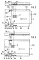
- Figure 2 is a chip card in a card reader at the removal position and communicating Mating contacts
- Figure 3 shows a chip card in a card reader in the end position with communicating mating contacts
- Figure 4a - 4c three positions of the sliding element when removing the Chip card from the end position to the withdrawal position
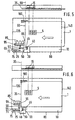
- Figure 5 shows a chip card in a card reader Withdrawal position with fixed counter contacts
- Figure 6 shows a chip card in a card reader in the end position with fixed counter contacts.
- 1 denotes a chip card with eight Contacts 5 on the surface of the chip card 1 with a microchip of the chip card 1 electrically connected are.
- the card reader has mating contacts 15 which are against press the contacts 5 of the chip card 1 and in this way the contacts 5 are electrically conductive with a computer 20 connect.
- the chip card 1 is in a End position 35 shown in dashed lines in the card reader and is from a first projection 55 of a sliding element 30th recorded in the card slot, not shown of the card reader protrudes.
- the sliding element 30 has a locking lug 40 which in a locking 50 a Guide rail 45 engages, the guide rail 45 parallel to that indicated by an arrow Insertion direction is and in the vicinity of the end position 35 the chip card 1 at right angles from the Guide rail 45 angled latch 50 opens.
- the Sliding element 30 has a second projection 65 in parallel to the direction of insertion to the card slot floor of the card reader towards.
- the second protrusion 65 is vertical to the direction of insertion and in the card reader attached first spring 60 against a first shift lever 70 a first switching arrangement 25 pressed so that the first Shift lever 70 with a second shift lever 75 of the first Switching arrangement 25 contacted. At the same time presses first spring 60 the latch 40 into the latch 50.
- the first Switching arrangement 25 is connected to the computer 20.
- the Chip card 1 presses the sliding element 30 opposite edge 120 against a first Shift lever 105 of a second shift arrangement 100, which at removed chip card 1 in the card slot of the Card reader protrudes and its position in this case is shown in dashed lines.
- the first shift lever 105 of the second switching arrangement 100 makes contact when inserted Chip card 1 according to FIG. 1 with a second switching lever 110 of the second switching arrangement 100.
- the second Switch arrangement 100 is also connected to computer 20 connected and also connected to a battery 115, which supplies the computer 20 with voltage.
- the Computer 20 By closing the first switching arrangement 25, the Computer 20 communicated that a chip card 1 in Card reader is located. The computer 20 can then read and / or Write operations on the microchip of the chip card 1 start. By opening the first switching arrangement 25 the Computer 20 announced the removal of the chip card 1, so that current read and / or write operations properly ended or no new reading and / or writing process starts.
- the second switching arrangement 100 When the chip card 1 is inserted into the card reader first closed the second switching arrangement 100 because it is in front of the end position 35 and therefore actuated is before the chip card 1 reaches the end position 35 and the first switching arrangement 25 can be actuated.
- Wise can be used for card readers who also have a Have "sleep function", reduce power consumption.
- the battery 115 becomes in time before the first one is actuated Switching arrangement 25 switched on, so that the computer 20 a Chip card 1 located in end position 35 in the card reader can detect.
- the arrangement of the second switching arrangement 100 reached before the end position 35; that even when the chip card 1 is removed, the battery 115 is not immediately turned off and thus the computer 20 still energy to properly end a current Get the writing and / or reading process from the battery 115 can.
- the second switching arrangement 100 Instead of turning the battery 115 on or off the second switching arrangement 100 enables the computer 20 through the second switching arrangement 100 into a through low power consumption marked rest position Removal of the chip card 1 are brought.
- the Chip card 1 is then activated by pressing the second one Switching arrangement 100 for reading and / or Write operations on the microchip of the chip card 1 required power supply switched on.
- the first spring 60 and the second projection 65 on the Chip card 1 facing side of the first switching arrangement 25 there is the first spring 60 and the second projection 65 on the Chip card 1 facing side of the first switching arrangement 25.
- the first shift lever 70 is the first Switching arrangement 25 facing the chip card 1 and the second Shift lever 75 of the first shift arrangement 25 is the Chip card 1 turned away.
- this is Sliding element 30 for engaging and actuating the first switching arrangement 25 pushed away from chip card 1, for which the rest 50 in facing away from the chip card 1
- Direction of the guide rail 45 is angled.
- Conceivable would also be one in the direction of the chip card 1 of the Guide rail 45 angled detent 50, then the first spring 60 for engaging the sliding element 30 in the Rest 50 with the second projection 65 the second Switch lever 75 on the side facing away from the chip card 1 first shift arrangement 25 against the first shift lever 70 must press for contacting and the first spring 60 on the the chip card 1 facing away from the first Switch arrangement 25 mounted vertically to the direction of insertion. have to be.
- the second projection 65 must then also on the the chip card 1 facing away from the first Switching arrangement 25 can be attached to the sliding element 30.
- FIG 2 is a card slot 10 of the card reader shown, in which the chip card 1 in a by Dashed line marked removal position 90 is inserted. It protrudes from the kart shaft 10 and can therefore be easily removed by hand.
- the counter-contacts 15 are communicating, so that even in the removal position 90, the contacts 5 in the middle are contacted by the counter contacts 15 of the card reader.
- the second switching arrangement 100 is closed because the Chipcard 1 with its edge 120, which is opposite the Sliding element 30 is arranged, still against the first Shift lever 105 of the second shift arrangement 100 presses so that the two shift levers 105 and 110 of the second Contact switching arrangement 100 with each other.
- the computer 20 is also used when the chip card 1 is removed still at least up to the removal position 90 with energy supplied, so that a current write and / or read operation can be ended properly.
- Figure 2 is closed remove that the sliding element 30 from an outer side 80th the card reader is accessible, for which purpose the outside 80 of the Card reader has an opening, not shown, in which the sliding element 30 parallel to the direction of insertion is movable from the outside.
- the sliding element 30 can only on the by the length of the guide rail 45th specified route to be moved.
- the Removal position 90 is the latch 40 of the Sliding element 30 already at that of the insertion opening 140 the card slot 10 facing limitation of Guide rail 45 so that the sliding element 30 does not continue can be moved in the removal direction.
- the chip card 1 is in the removal position 90 already protrudes from the card slot 10 for removal.
- the catch 40 is now in the guide rail 45, is the sliding element 30 compared to the engaged 1 shifted towards the chip card 1, so that the second projection 65 the first shift lever 70 of the first Switching arrangement 25 no longer against the second Shift lever 75 of the first shift arrangement 25 presses and first switching arrangement 25 is thus open.
- the first shift lever 70 becomes the first switching arrangement 25, for example, by a not in 2 shown further spring of the second Shift lever 75 of first shift arrangement 25 pushed away, the spring force of the further spring is smaller than that Spring force of the first spring must be 60 so that the Switch actuation works in the manner described.
- the first spring 60 is stationary in the card slot 10 of the Card reader attached, the second projection 65 so must be long that the removal position 90 of the Chip card 1, the first spring 60 on the second projection 65 rests and cannot slide off the second projection 65.
- the connection between the first spring 60 and the second Projection 65 is loose, so that the sliding element 30th can be moved against the first spring 60.
- the first shift lever 105 tilts second switching arrangement 100 for opening the second Switch arrangement 100 a bit down in the Card slot 10, for example supported by the spring force of a further spring, not shown.
- the card slot 10 in Height of the sliding element 30 has damping means 125, which are arranged parallel to the direction of insertion and the delay the sliding movement of the sliding member 30 to the to end current write and / or read processes time on the microchip of chip card 1 ensure that the microchip or of the computer 20 is avoided.
- Figure 3 shows the chip card 1 in the card slot 10 in the End position 35, the contacts 5 through the communicating Mating contacts 15 are contacted in the middle. Otherwise corresponds to the arrangement of Figure 3 according to the illustration Figure 1.
- the second switching arrangement 100 is first open, d. H. the first shift lever 105 of the second Switching arrangement 100 hangs as dashed in FIG. 2 shown in the card slot 10. Finally the sliding element 30 is in the position shown in FIG shown position of the removal position 90. Shortly before The chip card 1 is also pressed when the removal position 90 is reached its edge 120 lying opposite the sliding element 30 against the first shift lever 105 of the second Switch assembly 100 so that it matches the second Shift lever 110 of the second shift arrangement 100 contacted and turns on the battery 115.
- the first one Shift lever 105 of the second shift arrangement 100 from one Rounding 130 of edge 120 of chip card 1 is initially detected and when the chip card 1 is inserted further along the Rounding 130 led to the edge 120, where he then with the second shift lever 110 of the second shift arrangement 100 contacted.
- the battery 115 thus turned on the computer 20 for the detection of a complete inserted chip card prepared.
- the chip card 1 reached the removal position 90, it is from the first Projection 55 of the sliding element 30 is detected.
- the Sliding element 30 is then in with the chip card 1
- the direction of insertion is also moved, the catch 40 in the Guide rail 45 slides.
- the sliding element 30 is by the first Spring 60 with the detent 40 pressed into the detent 50 and the first switching arrangement 25 closed.
- the chip card 1 is then in the end position 35 and the computer 20 detects the fully inserted chip card 1 and can with read and / or write operations on the microchip the chip card 1 begin.
- the Sliding element 30 is this at the same time around the rest path from the opening of the outside 80 of the card slot 10 pressed.
- the position of the chip card 1 remains unchanged, for example by a corresponding in the guide, not shown in the figures, in the card slot 20 is achieved. This way the second one remains Switch arrangement 100 even when fully inserted Chip card 1 still closed.
- the mating contacts 15 are not communicating but rigidly connected to the card reader.
- the card slot floor 135, which is the Insertion opening 140 of the card slot 10 is opposite, a second spring 85 attached in the direction of insertion and in Card reader attached against the first projection 55 of the Pushing element 30 presses and optionally with this connected is.
- Parallel to the second spring 85 are others Damping means 95 mounted in the card slot 10.
- the Damping means 125 for the sliding element 30 according to the Figures 2 and 3 are not in Figure 5 and Figure 6 are shown, however, in addition to the others Damping means 95 may be present.
- the insert and the removal of the chip card 1 takes place in the described manner, wherein the insertion of the chip card 1 in the card slot 10 against the spring force of the second Spring 85 takes place and the displacement of the chip card 1 Removal from the end position 35 to the removal position 90 by the force of the preloaded second spring 85 is supported or executed.
- the delayed shutdown of battery 115 by the second Switching arrangement 100 can be used as a subfunction of the second Circuit arrangement 100 by means of a computer 20 interacting delay circuit also electronic take place, the delay circuit by opening the first switching arrangement 25 is activated.
- first switching arrangement 25 is namely already at the beginning of Unlatching process opened so that the further course of the Unlatching contributes to the required delay, especially since it takes place against the spring force of the first spring 60.
Landscapes
- Engineering & Computer Science (AREA)
- Artificial Intelligence (AREA)
- Computer Vision & Pattern Recognition (AREA)
- Physics & Mathematics (AREA)
- General Physics & Mathematics (AREA)
- Theoretical Computer Science (AREA)
- Details Of Connecting Devices For Male And Female Coupling (AREA)
- Coupling Device And Connection With Printed Circuit (AREA)
- Conveying Record Carriers (AREA)
Claims (10)
- Lecteur de cartes à puce (1) comportant une puce et des contacts (5) à la surface de la carte à puce (1), un logement à carte (10) pour recevoir et bloquer mécaniquement la carte à puce (1) ainsi que des contacts complémentaires (15) pour coopérer mécaniquement avec les contacts (5) de la puce et réaliser la liaison électrique entre un calculateur (20) et la puce, avec un premier circuit (25) mis en oeuvre par la présence ou l'absence de la carte à puce (1) dans le logement de carte (10),
lecteur dans lequel un élément coulissant (30) est déplacé par la carte à puce (1) dans le logement de carte (10), en étant guidé parallèlement à la direction d'introduction de la carte à puce dans le logement de carte (10), cet élément coulissant (30) s'accroche lorsque la carte à puce (1) occupe une position de fin de course (35) dans le logement de carte (10), puis
l'élément coulissant (30) actionne le premier circuit (25) lorsque la carte à puce (1) occupe la position de fin de course (35), et
l'élément coulissant (30) comporte un bec d'accrochage (40) qui pénètre dans un rail de guidage (45) dirigé dans la direction d'introduction,
caractérisé en ce que
l'élément coulissant parcourt un chemin d'accrochage au moment de son accrochage sans que la position de la carte à puce (1) ne change. - Lecteur de carte selon la revendication 1,
caractérisé en ce que
le rail de guidage (45) débouche à proximité de la position de fin de course (35) de la carte à puce (1) dans un logement recourbé (55) par rapport au rail de guidage (45), logement dans lequel s'accroche le bec d'accrochage (40). - Lecteur de carte selon la revendication 1 ou 2,
caractérisé en ce que
l'élément coulissant (30) comporte une première partie en saillie (55) pénétrant dans le logement de carte (10) et qui sert à extraire la carte à puce (1). - Lecteur de carte selon l'une des revendications précédentes,
caractérisé en ce que
le bec d'accrochage (40) de l'élément coulissant (30) est poussé dans le logement (50) par un premier ressort (60) lorsque la carte à puce (1) occupe la position de fin de course (35). - Lecteur de carte selon l'une des revendications précédentes,
caractérisé en ce que
l'élément coulissant (30) comporte une seconde partie en saillie (65) dans la direction d'introduction,
la seconde partie en saillie (65) pouvant être poussée par le premier ressort (60) contre un premier levier de commutation (70) du premier circuit de commutation (25) lorsque la carte à puce (1) occupe la position de fin course (35) pour que le premier levier de commutation (70) entre en contact avec un second levier de commutation (75) du premier circuit (25). - Lecteur de carte selon l'une des revendications précédentes,
caractérisé en ce que
l'élément coulissant (30) est accessible au niveau d'un côté extérieur (80) du lecteur de carte et lorsque la carte à puce (1) occupe la position de fin de course (35) il peut être déverrouillé contre la force développée par le premier ressort (60). - Lecteur de carte selon l'une des revendications 3 à 6,
caractérisé en ce que
lorsque la carte à puce (1) occupe la position de fin de course (35), la première partie en saillie (55) pousse contre un second ressort (85) dans la direction d'introduction, et
le second ressort (85) permet de conduire la carte à puce (1) de la position de fin de course (35) à la position d'extraction (90) après le déverrouillage. - Lecteur de carte selon la revendication 7,
caractérisé par
des moyens d'amortissement (95, 125) prévus dans la direction d'introduction qui retardent le coulissement de la carte à puce à partir de la position de fin de course (35) jusqu'au moins dans la position d'extraction (90). - Lecteur de carte selon l'une des revendications précédentes,
caractérisé par
un second circuit (100) actionné par la carte à puce (1) au moins entre la position de fin de course (35) et la position d'extraction (90). - Lecteur de carte selon l'une des revendications précédentes,
caractérisé en ce que
les contacts complémentaires (15) du lecteur de carte coopèrent avec le lecteur de carte pour qu'à l'extraction de la carte à puce (1) ils suivent jusqu'à la position d'extraction (90).
Applications Claiming Priority (2)
| Application Number | Priority Date | Filing Date | Title |
|---|---|---|---|
| DE19616316 | 1996-04-24 | ||
| DE19616316A DE19616316A1 (de) | 1996-04-24 | 1996-04-24 | Kartenleser für Chipkarten |
Publications (3)
| Publication Number | Publication Date |
|---|---|
| EP0803831A2 EP0803831A2 (fr) | 1997-10-29 |
| EP0803831A3 EP0803831A3 (fr) | 2000-08-23 |
| EP0803831B1 true EP0803831B1 (fr) | 2003-06-11 |
Family
ID=7792276
Family Applications (1)
| Application Number | Title | Priority Date | Filing Date |
|---|---|---|---|
| EP97101437A Expired - Lifetime EP0803831B1 (fr) | 1996-04-24 | 1997-01-30 | Lecteur de cartes à puce |
Country Status (2)
| Country | Link |
|---|---|
| EP (1) | EP0803831B1 (fr) |
| DE (2) | DE19616316A1 (fr) |
Families Citing this family (6)
| Publication number | Priority date | Publication date | Assignee | Title |
|---|---|---|---|---|
| FR2780182B1 (fr) * | 1998-06-22 | 2001-11-30 | Alsthom Cge Alkatel | Lecteur de carte a circuit integre |
| FR2797070B1 (fr) | 1999-07-30 | 2001-09-28 | St Microelectronics Sa | Lecture de carte a puce comprenant un systeme d'economie d'energie |
| DE10335646B4 (de) * | 2003-06-11 | 2007-04-19 | Yamaichi Electronics Deutschland Gmbh | Kartenleser mit Geräuschdämpfungseinrichtung |
| US7441709B2 (en) * | 2005-03-23 | 2008-10-28 | Endicott Interconnect Technologies, Inc. | Electronic card assembly |
| CN108256364B (zh) * | 2017-12-29 | 2020-12-29 | 浙江大华汽车技术有限公司 | 一种ic卡热插拔检测电路 |
| EP3584738B1 (fr) * | 2018-06-18 | 2023-01-04 | Ingenico Inc. | Lecteur de carte à puce de faible puissance |
Family Cites Families (2)
| Publication number | Priority date | Publication date | Assignee | Title |
|---|---|---|---|---|
| DE4332174A1 (de) * | 1993-09-22 | 1995-03-23 | Amphenol Tuchel Elect | Endlagenschalter für einen Chipkartenleser |
| FR2712414B1 (fr) * | 1993-11-09 | 1996-01-12 | Itt Composants Instr | Commutateur de détection de la présence d'une carte à mémoire électronique dans un dispositif de lecture de cartes. |
-
1996
- 1996-04-24 DE DE19616316A patent/DE19616316A1/de not_active Withdrawn
-
1997
- 1997-01-30 DE DE59710248T patent/DE59710248D1/de not_active Expired - Lifetime
- 1997-01-30 EP EP97101437A patent/EP0803831B1/fr not_active Expired - Lifetime
Also Published As
| Publication number | Publication date |
|---|---|
| EP0803831A2 (fr) | 1997-10-29 |
| DE19616316A1 (de) | 1997-10-30 |
| EP0803831A3 (fr) | 2000-08-23 |
| DE59710248D1 (de) | 2003-07-17 |
Similar Documents
| Publication | Publication Date | Title |
|---|---|---|
| DE69528036T2 (de) | Steckverbinder für eine miniatur gedruckte Platte | |
| DE69417945T2 (de) | IC-Karten-Verbindungsvorrichtung mit Schalter | |
| EP1740752B1 (fr) | Verrou pour appareil menager | |
| DE3302372A1 (de) | Schraubenlose klemme | |
| DE102009014584A1 (de) | Beweglicher Kontakthalter einer elektrischen Vorrichtung sowie Montageverfahren für einen beweglichen Kontakthalter | |
| EP0360345B1 (fr) | Dispositif de lecture pour carte à puce | |
| WO2021116129A1 (fr) | Composant de réception pour appareils électriques | |
| DE19519181C2 (de) | Schaltervorrichtung mit elektrisch ausgelöster Rückstellfunktion | |
| DE19616316A1 (de) | Kartenleser für Chipkarten | |
| DE4409456C2 (de) | Schalter | |
| EP2140395A2 (fr) | Lecteur de carte sim à tiroir blocable | |
| WO1997040466A1 (fr) | Dispositif de lecture de cartes | |
| DE102010011204A1 (de) | Schaltschrank und Geräteträger für einen Schaltschrank | |
| DE2025581A1 (de) | Mehrfach Kontaktsystem fur Nocken schalter | |
| DE10211925B4 (de) | Unterbrechervorrichtung | |
| EP2565896B1 (fr) | Interrupteur | |
| DE19757625B4 (de) | Chipkartenleser | |
| DE3731959C1 (en) | Device for ejecting slices of toast from an electric toaster | |
| DE19501641B4 (de) | Kartenleser für Chipkarten | |
| WO1996042186A1 (fr) | Systeme de panneau avant d'une carte a circuits imprimes pourvu d'un element integre a touche de commutation active/passive | |
| DE69215348T2 (de) | Schaltgeräte für elektromagnetische und manuelle Betätigung | |
| DE19734233A1 (de) | Berührungsschutzklappe für Sicherung | |
| DE102005017870A1 (de) | Verschluß für ein Hausgerät | |
| DE3842877A1 (de) | Schaltvorrichtung | |
| DE19503566B4 (de) | Chipkartenleser, insbesondere mit elektrischer Erkennung der Kontaktsatzverriegelung |
Legal Events
| Date | Code | Title | Description |
|---|---|---|---|
| PUAI | Public reference made under article 153(3) epc to a published international application that has entered the european phase |
Free format text: ORIGINAL CODE: 0009012 |
|
| AK | Designated contracting states |
Kind code of ref document: A2 Designated state(s): DE FR GB IT |
|
| PUAL | Search report despatched |
Free format text: ORIGINAL CODE: 0009013 |
|
| AK | Designated contracting states |
Kind code of ref document: A3 Designated state(s): DE FR GB IT |
|
| RIC1 | Information provided on ipc code assigned before grant |
Free format text: 7G 06K 7/06 A, 7G 06K 13/08 B, 7G 06K 7/00 B |
|
| 17P | Request for examination filed |
Effective date: 20010223 |
|
| 17Q | First examination report despatched |
Effective date: 20020514 |
|
| GRAH | Despatch of communication of intention to grant a patent |
Free format text: ORIGINAL CODE: EPIDOS IGRA |
|
| GRAH | Despatch of communication of intention to grant a patent |
Free format text: ORIGINAL CODE: EPIDOS IGRA |
|
| GRAA | (expected) grant |
Free format text: ORIGINAL CODE: 0009210 |
|
| AK | Designated contracting states |
Designated state(s): DE FR GB IT |
|
| REG | Reference to a national code |
Ref country code: GB Ref legal event code: FG4D Free format text: NOT ENGLISH |
|
| REF | Corresponds to: |
Ref document number: 59710248 Country of ref document: DE Date of ref document: 20030717 Kind code of ref document: P |
|
| GBT | Gb: translation of ep patent filed (gb section 77(6)(a)/1977) |
Effective date: 20031006 |
|
| PG25 | Lapsed in a contracting state [announced via postgrant information from national office to epo] |
Ref country code: GB Free format text: LAPSE BECAUSE OF NON-PAYMENT OF DUE FEES Effective date: 20040130 |
|
| ET | Fr: translation filed | ||
| PLBE | No opposition filed within time limit |
Free format text: ORIGINAL CODE: 0009261 |
|
| STAA | Information on the status of an ep patent application or granted ep patent |
Free format text: STATUS: NO OPPOSITION FILED WITHIN TIME LIMIT |
|
| 26N | No opposition filed |
Effective date: 20040312 |
|
| GBPC | Gb: european patent ceased through non-payment of renewal fee |
Effective date: 20040130 |
|
| PG25 | Lapsed in a contracting state [announced via postgrant information from national office to epo] |
Ref country code: FR Free format text: LAPSE BECAUSE OF NON-PAYMENT OF DUE FEES Effective date: 20040930 |
|
| REG | Reference to a national code |
Ref country code: FR Ref legal event code: ST |
|
| PG25 | Lapsed in a contracting state [announced via postgrant information from national office to epo] |
Ref country code: IT Free format text: LAPSE BECAUSE OF NON-PAYMENT OF DUE FEES Effective date: 20080130 |
|
| PGFP | Annual fee paid to national office [announced via postgrant information from national office to epo] |
Ref country code: IT Payment date: 20160122 Year of fee payment: 20 Ref country code: DE Payment date: 20160128 Year of fee payment: 20 |
|
| REG | Reference to a national code |
Ref country code: DE Ref legal event code: R071 Ref document number: 59710248 Country of ref document: DE |