EP0803896A2 - Plasma processing system and protective member used for the same - Google Patents
Plasma processing system and protective member used for the same Download PDFInfo
- Publication number
- EP0803896A2 EP0803896A2 EP97302744A EP97302744A EP0803896A2 EP 0803896 A2 EP0803896 A2 EP 0803896A2 EP 97302744 A EP97302744 A EP 97302744A EP 97302744 A EP97302744 A EP 97302744A EP 0803896 A2 EP0803896 A2 EP 0803896A2
- Authority
- EP
- European Patent Office
- Prior art keywords
- plasma
- electrodes
- protective member
- plasma processing
- glassy carbon
- Prior art date
- Legal status (The legal status is an assumption and is not a legal conclusion. Google has not performed a legal analysis and makes no representation as to the accuracy of the status listed.)
- Granted
Links
- 230000001681 protective effect Effects 0.000 title claims abstract description 37
- 229910021397 glassy carbon Inorganic materials 0.000 claims abstract description 32
- 239000003575 carbonaceous material Substances 0.000 claims abstract description 24
- 239000000428 dust Substances 0.000 abstract description 14
- 229910052782 aluminium Inorganic materials 0.000 description 13
- XAGFODPZIPBFFR-UHFFFAOYSA-N aluminium Chemical compound [Al] XAGFODPZIPBFFR-UHFFFAOYSA-N 0.000 description 13
- 239000002245 particle Substances 0.000 description 9
- 238000001020 plasma etching Methods 0.000 description 8
- 239000000463 material Substances 0.000 description 6
- 230000000052 comparative effect Effects 0.000 description 5
- 239000007789 gas Substances 0.000 description 5
- 238000000034 method Methods 0.000 description 5
- XUIMIQQOPSSXEZ-UHFFFAOYSA-N Silicon Chemical compound [Si] XUIMIQQOPSSXEZ-UHFFFAOYSA-N 0.000 description 4
- 238000005530 etching Methods 0.000 description 4
- 229910052710 silicon Inorganic materials 0.000 description 4
- 239000010703 silicon Substances 0.000 description 4
- OKTJSMMVPCPJKN-UHFFFAOYSA-N Carbon Chemical compound [C] OKTJSMMVPCPJKN-UHFFFAOYSA-N 0.000 description 3
- XPFVYQJUAUNWIW-UHFFFAOYSA-N furfuryl alcohol Chemical compound OCC1=CC=CO1 XPFVYQJUAUNWIW-UHFFFAOYSA-N 0.000 description 3
- 229910002804 graphite Inorganic materials 0.000 description 3
- 239000010439 graphite Substances 0.000 description 3
- 239000011347 resin Substances 0.000 description 3
- 229920005989 resin Polymers 0.000 description 3
- 239000004065 semiconductor Substances 0.000 description 3
- CSCPPACGZOOCGX-UHFFFAOYSA-N Acetone Chemical compound CC(C)=O CSCPPACGZOOCGX-UHFFFAOYSA-N 0.000 description 2
- XKRFYHLGVUSROY-UHFFFAOYSA-N Argon Chemical compound [Ar] XKRFYHLGVUSROY-UHFFFAOYSA-N 0.000 description 2
- XPDWGBQVDMORPB-UHFFFAOYSA-N Fluoroform Chemical compound FC(F)F XPDWGBQVDMORPB-UHFFFAOYSA-N 0.000 description 2
- 238000007743 anodising Methods 0.000 description 2
- 238000004891 communication Methods 0.000 description 2
- 239000007849 furan resin Substances 0.000 description 2
- 229910052751 metal Inorganic materials 0.000 description 2
- 239000002184 metal Substances 0.000 description 2
- 239000005011 phenolic resin Substances 0.000 description 2
- 238000005268 plasma chemical vapour deposition Methods 0.000 description 2
- 229910052786 argon Inorganic materials 0.000 description 1
- QVGXLLKOCUKJST-UHFFFAOYSA-N atomic oxygen Chemical compound [O] QVGXLLKOCUKJST-UHFFFAOYSA-N 0.000 description 1
- 230000015572 biosynthetic process Effects 0.000 description 1
- 229920002678 cellulose Polymers 0.000 description 1
- 239000001913 cellulose Substances 0.000 description 1
- 238000002474 experimental method Methods 0.000 description 1
- 229920005546 furfural resin Polymers 0.000 description 1
- 230000010354 integration Effects 0.000 description 1
- 238000004519 manufacturing process Methods 0.000 description 1
- 239000000203 mixture Substances 0.000 description 1
- 230000003287 optical effect Effects 0.000 description 1
- 230000003647 oxidation Effects 0.000 description 1
- 238000007254 oxidation reaction Methods 0.000 description 1
- 239000001301 oxygen Substances 0.000 description 1
- 229910052760 oxygen Inorganic materials 0.000 description 1
- 239000010453 quartz Substances 0.000 description 1
- 239000012495 reaction gas Substances 0.000 description 1
- VYPSYNLAJGMNEJ-UHFFFAOYSA-N silicon dioxide Inorganic materials O=[Si]=O VYPSYNLAJGMNEJ-UHFFFAOYSA-N 0.000 description 1
- 238000004381 surface treatment Methods 0.000 description 1
- 229920001187 thermosetting polymer Polymers 0.000 description 1
Images
Classifications
-
- H—ELECTRICITY
- H01—ELECTRIC ELEMENTS
- H01J—ELECTRIC DISCHARGE TUBES OR DISCHARGE LAMPS
- H01J37/00—Discharge tubes with provision for introducing objects or material to be exposed to the discharge, e.g. for the purpose of examination or processing thereof
- H01J37/32—Gas-filled discharge tubes
- H01J37/32431—Constructional details of the reactor
- H01J37/32458—Vessel
- H01J37/32477—Vessel characterised by the means for protecting vessels or internal parts, e.g. coatings
-
- H—ELECTRICITY
- H01—ELECTRIC ELEMENTS
- H01J—ELECTRIC DISCHARGE TUBES OR DISCHARGE LAMPS
- H01J37/00—Discharge tubes with provision for introducing objects or material to be exposed to the discharge, e.g. for the purpose of examination or processing thereof
- H01J37/32—Gas-filled discharge tubes
- H01J37/32431—Constructional details of the reactor
- H01J37/32623—Mechanical discharge control means
Definitions
- the present invention relates to a plasma processing system such as a plasma etching system or a plasma VCD system, e.g. used for production of semiconductor integrated circuits, such as LSIs or ICs, or waveguides for optical communication, and a protective member used for the plasma processing system.
- a plasma processing system such as a plasma etching system or a plasma VCD system, e.g. used for production of semiconductor integrated circuits, such as LSIs or ICs, or waveguides for optical communication, and a protective member used for the plasma processing system.
- a plasma processing technique such as a plasma etching technique or a plasma CVD technique, capable of forming a finer pattern on a wafer at a high accuracy has come to be increasingly important along with the advance of techniques for producing semiconductor integrated circuits with finer-geometries and higher densities.
- An electrode used for such a plasma processing technique has been made of aluminum, graphite, glassy carbon, metal silicon or quartz.
- parts of a plasma processing system such as a chamber or a member called “depo-shield” (protective member) have been generally made of aluminum, and in recent years, to meet requirements for high integration of semiconductors, these parts made of aluminum have come to be further subjected to surface treatment by anodic oxidation.
- a chamber or a protective member of a plasma processing system is made of aluminum as described, it is possibly brought in direct contact with plasma and also exposed to a corrosive gas to be thereby damaged, and such damage of the chamber or protective member causes the generation of dust in addition to the shortened service life. Therefore, it would be desirable to develop a new material for a chamber or a protective member capable of suppressing the damage thereof for preventing the generation of dust.
- Preferred embodiments of the present invention may provide a plasma processing system and a protective member used for the plasma processing system, which are capable of suppressing the generation of particles (dust) and prolonging the service life.
- a plasma processing system including a plasma processing chamber in which plasma generating electrodes are disposed, characterized in that at least a surface of an internal portion, exposed to plasma, of the plasma processing chamber excluding the electrodes is formed of a glassy carbon material.
- a protective member for a plasma processing system which is disposed in use in a plasma processing chamber containing two plasma generating electrodes for forming a plasma region between the electrodes, on the side of each of the two electrodes in such a manner as to cover the plasma region, characterized in that at least a surface of the protective member on the plasma region side is formed of a glassy carbon material.
- the plasma processing system of the present invention which is applicable for various types of plasma processing systems for processing workpieces by plasma, such as a plasma etching system or a plasma CVD system, is advantageous in that since at least a surface of a portion exposed to plasma, for example, a chamber wall surface or a plasma exposure portion of a protective member is formed of a glassy carbon material, it is suppressed from being eroded or damaged by plasma, as a result of which it is possible to prolong the service life thereof and also to suppress the generation of particles (dust) and hence to desirably prevent the adhesion of dust on a workpiece such as a wafer upon plasma etching.
- the entire member including the portion exposed to plasma may be formed of a glassy carbon material, although it is desired in terms of cost that the main body of the member is formed of a different material such as aluminum and the portion exposed to plasma or the entire member is covered with a glassy carbon material. Even when the main body of the member is made of aluminum, the member can be positively prevented from being eroded or damaged by plasma by covering at least a portion exposed to plasma with the glassy carbon material.
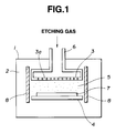
- Fig. 1 is a schematic view showing one embodiment of the present invention.
- Fig. 1 shows a plasma etching system to which the present invention is applied.
- reference numeral 1 indicates a main body of the processing system containing a plasma processing chamber 2.
- two plasma generating electrodes 3, 4 are oppositely spaced at a specified distance, and a plasma region 5 is formed between both the electrodes 3, 4.
- An etching gas feed pipe 6 is connected to one electrode (upper electrode) 3.
- An etching gas passes through the feed pipe 6, and is fed in the plasma region 5 from a plurality of etching gas communication holes 3a formed in the upper electrode 3.
- a workpiece 7, for example, a silicon wafer is placed on the other electrode (lower electrode) 4.
- the upper electrode 3 is connected to a high frequency power supply and the lower electrode 4 is grounded.
- Protective members 8, 8 are respectively disposed outside both the electrodes 3, 4 in such a manner as to cover the plasma region 5.
- each of the protective member 8, 8 on the plasma region 5 side is formed of a glassy carbon material.
- the protective member may be entirely formed of a glassy carbon material.
- the protective member may be formed of aluminum or the like, and the entire surface of the protective member or a surface thereof on the plasma region side may be covered with a glassy carbon material.
- the covering of the glassy carbon material can be performed by forming a glassy carbon material in the form of a film, and sticking the film on the target portion.
- the thickness of the glassy carbon film may be in a range of from 10 ⁇ m to 10 mm, preferably, in a range of from 50 ⁇ m to 6 mm.
- source materials of the above glassy carbon material include cellulose, furfuryl alcohol, phenol resin, acetone, polycarbodiimide resin, furan resin, furfural resin, other thermosetting resins, and mixtures thereof.
- the electrode may be formed of a known material, but it may be preferably formed of a glassy carbon or metal silicon.
- the main body of the system may be formed of a known material such as aluminum.
- the inner wall surface of the main body of the system may be entirely covered with a glassy carbon material, or a surface portion of the main body of the system which is possibly exposed to plasma leaked from gaps between both the electrodes and the protective members may be covered with a glassy carbon material.
- the protective members are not provided in the chamber, the entire inner wall surface of the main body of the system or a portion exposed to plasma is covered with a glassy carbon material.
- the plasma etching system shown in Fig. 1 is usable for a long period of time in accordance with the normal processing manner while significantly suppressing the generation of particles (dust) because the protective members, in which the surfaces on the plasma resin side are formed of the glassy carbon material, are prevented from being eroded or damaged by plasma.
- a protective member sample having a shape shown in Fig. 1 was prepared using a glassy carbon material (density: 1.51 g/cm 3 , total ash: 2 ppm) produced from phenol resin.
- a protective member sample having a shape shown in Fig. 1 was prepared by sticking a glassy carbon film (density: 1.55 g/cm 3 , total ash: 20 ppm, thickness: 0.35 mm) on the surface of a protective member on the plasma region side.
- the glassy carbon film was produced from polycarbodiimide, and the protective member was formed of aluminum, followed by anodising treatment.
- a protective member having a shape shown in Fig. 1 was prepared using a glassy carbon material (density: 1.52 g/cm 3 , total ash: 10 ppm) produced by furan resin.
- the protective member which was formed of aluminum, followed by anodising treatment in Example 2, was used as a protective member sample.
- a protective member sample having a shape shown in Fig. 1 was prepared using an isotropic graphite (density: 1.85 g/cm 3 ).
- each of the above protective member samples was set into the plasma etching system shown in Fig. 1 in the manner shown in Fig. 1, and an oxide film on a silicon wafer (diameter: 8 inch (20cm)) was etched by plasma using a mixed gas of trifluoromethane as a reaction gas, argon and oxygen. After this etching, the number of particles (particle size: 0.3 ⁇ m or more) adhering on the surface of the wafer was counted. The results are shown in Table 1. In this experiment, a plasma generating electrode formed of a glassy carbon material was used as the electrode, and the main body of the system was formed of aluminum.
- each of the protective member samples in Examples 1 to 3 is significantly small in the number of particles (dust) adhering on the surface of the wafer even at the 1500-th processing, as compared with the protective member samples in Comparative Examples 1 and 2.
- Table 1 material shape number of particles (dust) on wafer at the 10-th processing number of particles (dust) on wafer at the 1500-th processing
- Example 1 glassy carbon single body 4 4
- Example 2 glassy carbon stuck on surface of member (aluminum, alumite treated) 5 3
Landscapes
- Physics & Mathematics (AREA)
- Engineering & Computer Science (AREA)
- Plasma & Fusion (AREA)
- Chemical & Material Sciences (AREA)
- Analytical Chemistry (AREA)
- Drying Of Semiconductors (AREA)
- ing And Chemical Polishing (AREA)
- Chemical Vapour Deposition (AREA)
Abstract
Description
- The present invention relates to a plasma processing system such as a plasma etching system or a plasma VCD system, e.g. used for production of semiconductor integrated circuits, such as LSIs or ICs, or waveguides for optical communication, and a protective member used for the plasma processing system.
- In recent years, a plasma processing technique, such as a plasma etching technique or a plasma CVD technique, capable of forming a finer pattern on a wafer at a high accuracy has come to be increasingly important along with the advance of techniques for producing semiconductor integrated circuits with finer-geometries and higher densities.
- An electrode used for such a plasma processing technique has been made of aluminum, graphite, glassy carbon, metal silicon or quartz.
- On the other hand, parts of a plasma processing system, such as a chamber or a member called "depo-shield" (protective member), have been generally made of aluminum, and in recent years, to meet requirements for high integration of semiconductors, these parts made of aluminum have come to be further subjected to surface treatment by anodic oxidation.
- Incidentally, in the case of processing a wafer by plasma etching or the like, the adhesion of dust on the surface of the wafer is undesirable. Such dust has been considered to result from scattering of particles of electrodes when the electrodes are eroded and consumed by plasma, and attempts have been made to suppress the generation of dust from electrodes. However, as a result of various examinations made by the present inventor, it has been found that such dust is caused not only by electrodes but also by a plasma processing system itself.
- Specifically, although a chamber or a protective member of a plasma processing system is made of aluminum as described, it is possibly brought in direct contact with plasma and also exposed to a corrosive gas to be thereby damaged, and such damage of the chamber or protective member causes the generation of dust in addition to the shortened service life. Therefore, it would be desirable to develop a new material for a chamber or a protective member capable of suppressing the damage thereof for preventing the generation of dust.
- Preferred embodiments of the present invention may provide a plasma processing system and a protective member used for the plasma processing system, which are capable of suppressing the generation of particles (dust) and prolonging the service life.
- According to a first aspect of the present invention, there is provided a plasma processing system including a plasma processing chamber in which plasma generating electrodes are disposed, characterized in that at least a surface of an internal portion, exposed to plasma, of the plasma processing chamber excluding the electrodes is formed of a glassy carbon material.
- According to a second aspect of the present invention, there is provided a protective member for a plasma processing system, which is disposed in use in a plasma processing chamber containing two plasma generating electrodes for forming a plasma region between the electrodes, on the side of each of the two electrodes in such a manner as to cover the plasma region, characterized in that at least a surface of the protective member on the plasma region side is formed of a glassy carbon material.
- The plasma processing system of the present invention, which is applicable for various types of plasma processing systems for processing workpieces by plasma, such as a plasma etching system or a plasma CVD system, is advantageous in that since at least a surface of a portion exposed to plasma, for example, a chamber wall surface or a plasma exposure portion of a protective member is formed of a glassy carbon material, it is suppressed from being eroded or damaged by plasma, as a result of which it is possible to prolong the service life thereof and also to suppress the generation of particles (dust) and hence to desirably prevent the adhesion of dust on a workpiece such as a wafer upon plasma etching.
- In addition, as for the formation of a portion exposed to plasma of a glassy carbon material, the entire member including the portion exposed to plasma may be formed of a glassy carbon material, although it is desired in terms of cost that the main body of the member is formed of a different material such as aluminum and the portion exposed to plasma or the entire member is covered with a glassy carbon material. Even when the main body of the member is made of aluminum, the member can be positively prevented from being eroded or damaged by plasma by covering at least a portion exposed to plasma with the glassy carbon material.
- The present invention disclosed herein will be understood better with reference to the following drawing of which:
- Fig. 1 is a schematic view showing one embodiment of the present invention.
- An embodiment of the present invention will be described with reference to the accompanying drawing.
- Fig. 1 shows a plasma etching system to which the present invention is applied. In this figure, reference numeral 1 indicates a main body of the processing system containing a
plasma processing chamber 2. In thisplasma processing chamber 2, two plasma generatingelectrodes plasma region 5 is formed between both theelectrodes gas feed pipe 6 is connected to one electrode (upper electrode) 3. An etching gas passes through thefeed pipe 6, and is fed in theplasma region 5 from a plurality of etching gas communication holes 3a formed in theupper electrode 3. Aworkpiece 7, for example, a silicon wafer is placed on the other electrode (lower electrode) 4. In addition, while not shown, theupper electrode 3 is connected to a high frequency power supply and thelower electrode 4 is grounded. -
Protective members electrodes plasma region 5. - In accordance with the present invention, at least a surface of each of the
protective member plasma region 5 side is formed of a glassy carbon material. The protective member may be entirely formed of a glassy carbon material. Alternatively, the protective member may be formed of aluminum or the like, and the entire surface of the protective member or a surface thereof on the plasma region side may be covered with a glassy carbon material. The covering of the glassy carbon material can be performed by forming a glassy carbon material in the form of a film, and sticking the film on the target portion. The thickness of the glassy carbon film may be in a range of from 10 µm to 10 mm, preferably, in a range of from 50 µm to 6 mm. - Specific examples of source materials of the above glassy carbon material include cellulose, furfuryl alcohol, phenol resin, acetone, polycarbodiimide resin, furan resin, furfural resin, other thermosetting resins, and mixtures thereof.
- The electrode may be formed of a known material, but it may be preferably formed of a glassy carbon or metal silicon. In the case of providing the protective members treated as described above, the main body of the system may be formed of a known material such as aluminum. Of course, the inner wall surface of the main body of the system may be entirely covered with a glassy carbon material, or a surface portion of the main body of the system which is possibly exposed to plasma leaked from gaps between both the electrodes and the protective members may be covered with a glassy carbon material. On the other hand, in the case where the protective members are not provided in the chamber, the entire inner wall surface of the main body of the system or a portion exposed to plasma is covered with a glassy carbon material.
- The plasma etching system shown in Fig. 1 is usable for a long period of time in accordance with the normal processing manner while significantly suppressing the generation of particles (dust) because the protective members, in which the surfaces on the plasma resin side are formed of the glassy carbon material, are prevented from being eroded or damaged by plasma.
- Although the description has been made with respect to the system shown in Fig. 1, such description is for illustrative purposes only, and it is to be noted that the present invention is applicable for other known processing systems and further other processing steps may be variously changed within the scope of the present invention.
- The present invention will be more clearly understood with reference to the following examples:
- A protective member sample having a shape shown in Fig. 1 was prepared using a glassy carbon material (density: 1.51 g/cm3, total ash: 2 ppm) produced from phenol resin.
- A protective member sample having a shape shown in Fig. 1 was prepared by sticking a glassy carbon film (density: 1.55 g/cm3, total ash: 20 ppm, thickness: 0.35 mm) on the surface of a protective member on the plasma region side. The glassy carbon film was produced from polycarbodiimide, and the protective member was formed of aluminum, followed by anodising treatment.
- A protective member having a shape shown in Fig. 1 was prepared using a glassy carbon material (density: 1.52 g/cm3, total ash: 10 ppm) produced by furan resin.
- The protective member, which was formed of aluminum, followed by anodising treatment in Example 2, was used as a protective member sample.
- A protective member sample having a shape shown in Fig. 1 was prepared using an isotropic graphite (density: 1.85 g/cm3).
- Next, each of the above protective member samples was set into the plasma etching system shown in Fig. 1 in the manner shown in Fig. 1, and an oxide film on a silicon wafer (diameter: 8 inch (20cm)) was etched by plasma using a mixed gas of trifluoromethane as a reaction gas, argon and oxygen. After this etching, the number of particles (particle size: 0.3 µm or more) adhering on the surface of the wafer was counted. The results are shown in Table 1. In this experiment, a plasma generating electrode formed of a glassy carbon material was used as the electrode, and the main body of the system was formed of aluminum.
- From the results shown in Table 1, it is revealed that each of the protective member samples in Examples 1 to 3 is significantly small in the number of particles (dust) adhering on the surface of the wafer even at the 1500-th processing, as compared with the protective member samples in Comparative Examples 1 and 2.
Table 1 material shape number of particles (dust) on wafer at the 10-th processing number of particles (dust) on wafer at the 1500-th processing Example 1 glassy carbon single body 4 4 Example 2 glassy carbon stuck on surface of member (aluminum, alumite treated) 5 3 Example 3 glassy carbon single body 3 5 Comparative Example 1 aluminum, alumite treated single body 10 250 Comparative Example 2 isotropic graphite single body 140 300
Claims (5)
- A plasma processing system including a plasma processing chamber in which plasma generating electrodes are disposed, wherein at least a surface of an internal portion, exposed to plasma, of said plasma processing chamber excluding said electrodes is formed of a glassy carbon material.
- A protective member for a plasma processing system, which is disposed in use in a plasma processing chamber containing two plasma generating electrodes for forming a plasma region between said electrodes, on the side of each of said two electrodes in such a manner as to cover said plasma region, wherein at least a surface of said protective member on the plasma region side is formed of a glassy carbon material.
- A plasma processing system comprising a plasma processing chamber containing two plasma generating electrodes for forming a plasma region between said electrodes, and at least one protective member as defined in claim 2 disposed at the side of said two electrodes in such a manner as to cover said plasma region.
- A plasma processing system according to claim 3 having a pair of said protective members disposed at respective sides of said electrodes.
- A plasma processing system according to claim 3 or claim 4 wherein at least a surface of an internal portion, exposed to plasma, of said plasma processing chamber excluding said electrodes is formed of a glassy carbon material.
Applications Claiming Priority (3)
| Application Number | Priority Date | Filing Date | Title |
|---|---|---|---|
| JP12407596A JP3444090B2 (en) | 1996-04-22 | 1996-04-22 | Protective member for plasma processing equipment |
| JP124075/96 | 1996-04-22 | ||
| JP12407596 | 1996-04-22 |
Publications (3)
| Publication Number | Publication Date |
|---|---|
| EP0803896A2 true EP0803896A2 (en) | 1997-10-29 |
| EP0803896A3 EP0803896A3 (en) | 1998-07-15 |
| EP0803896B1 EP0803896B1 (en) | 2004-01-07 |
Family
ID=14876321
Family Applications (1)
| Application Number | Title | Priority Date | Filing Date |
|---|---|---|---|
| EP97302744A Expired - Lifetime EP0803896B1 (en) | 1996-04-22 | 1997-04-22 | Plasma processing system and protective member used for the same |
Country Status (5)
| Country | Link |
|---|---|
| EP (1) | EP0803896B1 (en) |
| JP (1) | JP3444090B2 (en) |
| KR (1) | KR970070243A (en) |
| DE (1) | DE69727094T2 (en) |
| TW (1) | TW425437B (en) |
Cited By (4)
| Publication number | Priority date | Publication date | Assignee | Title |
|---|---|---|---|---|
| WO2001052303A1 (en) * | 2000-01-11 | 2001-07-19 | E.I. Dupont De Nemours And Company | Liner for semiconductor etching chamber |
| US6383333B1 (en) * | 1998-04-28 | 2002-05-07 | Tokai Carbon Company, Ltd. | Protective member for inner surface of chamber and plasma processing apparatus |
| US6660093B2 (en) * | 2000-05-25 | 2003-12-09 | Kabushiki Kaisha Kobe Seiko Sho (Kobe Steel, Ltd.) | Inner tube for CVD apparatus |
| US7485239B2 (en) | 2002-08-06 | 2009-02-03 | Kobe Steel, Ltd | Component of glass-like carbon for CVD apparatus and process for production thereof |
Families Citing this family (2)
| Publication number | Priority date | Publication date | Assignee | Title |
|---|---|---|---|---|
| KR100733121B1 (en) * | 2000-09-07 | 2007-06-27 | 삼성전자주식회사 | Dry etching equipment |
| WO2007058605A1 (en) * | 2005-11-18 | 2007-05-24 | Replisaurus Technologies Ab | Master electrode and method of forming it |
Family Cites Families (8)
| Publication number | Priority date | Publication date | Assignee | Title |
|---|---|---|---|---|
| JPS58213427A (en) * | 1982-06-04 | 1983-12-12 | Hitachi Ltd | plasma etching equipment |
| JP3215978B2 (en) * | 1990-11-30 | 2001-10-09 | 日清紡績株式会社 | Method for producing glassy carbon coating |
| JP2936790B2 (en) * | 1991-05-27 | 1999-08-23 | 株式会社島津製作所 | Thin film forming equipment |
| JPH05304114A (en) * | 1992-04-28 | 1993-11-16 | Hitachi Chem Co Ltd | Electrode plate for plasma etching |
| JPH07122540A (en) * | 1993-10-25 | 1995-05-12 | Tokyo Electron Ltd | Etching equipment |
| US5680013A (en) * | 1994-03-15 | 1997-10-21 | Applied Materials, Inc. | Ceramic protection for heated metal surfaces of plasma processing chamber exposed to chemically aggressive gaseous environment therein and method of protecting such heated metal surfaces |
| JP3262696B2 (en) * | 1995-09-18 | 2002-03-04 | 信越石英株式会社 | Silica glass member having glassy carbon coating |
| EP0763504B1 (en) * | 1995-09-14 | 1999-06-02 | Heraeus Quarzglas GmbH | Silica glass member and method for producing the same |
-
1996
- 1996-04-22 JP JP12407596A patent/JP3444090B2/en not_active Expired - Fee Related
-
1997
- 1997-04-17 TW TW086104964A patent/TW425437B/en not_active IP Right Cessation
- 1997-04-22 KR KR1019970014841A patent/KR970070243A/en not_active Ceased
- 1997-04-22 DE DE69727094T patent/DE69727094T2/en not_active Expired - Fee Related
- 1997-04-22 EP EP97302744A patent/EP0803896B1/en not_active Expired - Lifetime
Cited By (4)
| Publication number | Priority date | Publication date | Assignee | Title |
|---|---|---|---|---|
| US6383333B1 (en) * | 1998-04-28 | 2002-05-07 | Tokai Carbon Company, Ltd. | Protective member for inner surface of chamber and plasma processing apparatus |
| WO2001052303A1 (en) * | 2000-01-11 | 2001-07-19 | E.I. Dupont De Nemours And Company | Liner for semiconductor etching chamber |
| US6660093B2 (en) * | 2000-05-25 | 2003-12-09 | Kabushiki Kaisha Kobe Seiko Sho (Kobe Steel, Ltd.) | Inner tube for CVD apparatus |
| US7485239B2 (en) | 2002-08-06 | 2009-02-03 | Kobe Steel, Ltd | Component of glass-like carbon for CVD apparatus and process for production thereof |
Also Published As
| Publication number | Publication date |
|---|---|
| JPH09289198A (en) | 1997-11-04 |
| DE69727094T2 (en) | 2004-09-09 |
| JP3444090B2 (en) | 2003-09-08 |
| KR970070243A (en) | 1997-11-07 |
| EP0803896B1 (en) | 2004-01-07 |
| TW425437B (en) | 2001-03-11 |
| DE69727094D1 (en) | 2004-02-12 |
| EP0803896A3 (en) | 1998-07-15 |
Similar Documents
| Publication | Publication Date | Title |
|---|---|---|
| EP1336191B1 (en) | Stepped upper electrode for plasma processing uniformity | |
| US7646581B2 (en) | Electrostatic chuck | |
| EP1081749B1 (en) | Protective member for inner surface of chamber and plasma processing apparatus | |
| EP0791956B1 (en) | Electrostatic chuck | |
| KR100632643B1 (en) | Plasma resistant member and plasma processing apparatus using the same | |
| EP3171393B1 (en) | Sealed elastomer bonded si electrodes and the like for reduced particle contamination in dielectric etch and method of manufacturing such electrodes | |
| EP0803897B1 (en) | Electrode for plasma etching; apparatus and process using such electrode | |
| CN100555550C (en) | Method and apparatus for an improved upper electrode plate in a plasma processing system | |
| KR100980972B1 (en) | Plasma treatment apparatus and plasma treatment method | |
| US8038837B2 (en) | Ring-shaped component for use in a plasma processing, plasma processing apparatus and outer ring-shaped member | |
| EP0803896A2 (en) | Plasma processing system and protective member used for the same | |
| EP0803895A2 (en) | Electrode for plasma etching | |
| JP2007207840A (en) | Susceptor arrangement | |
| JP3444089B2 (en) | Plasma etching electrode | |
| US7344652B2 (en) | Plasma etching method | |
| JP3674282B2 (en) | Plasma generating apparatus, chamber inner wall protecting member and manufacturing method thereof, chamber inner wall protecting method and plasma processing method | |
| US6051099A (en) | Apparatus for achieving etch rate uniformity | |
| JPH09289195A (en) | Plasma etching electrode | |
| JPH05234947A (en) | Microwave plasma etching device | |
| KR100459646B1 (en) | Separable shield ring | |
| JPH11219935A (en) | Electrode for plasma processor and the plasma processor | |
| JPH08148471A (en) | Plasma etching equipment | |
| KR100293460B1 (en) | Semiconductor device manufacturing method | |
| JPH07273094A (en) | Plasma etching electrode plate | |
| JPH09289199A (en) | Plasma etching electrode |
Legal Events
| Date | Code | Title | Description |
|---|---|---|---|
| PUAI | Public reference made under article 153(3) epc to a published international application that has entered the european phase |
Free format text: ORIGINAL CODE: 0009012 |
|
| AK | Designated contracting states |
Kind code of ref document: A2 Designated state(s): DE FR GB |
|
| PUAL | Search report despatched |
Free format text: ORIGINAL CODE: 0009013 |
|
| AK | Designated contracting states |
Kind code of ref document: A3 Designated state(s): DE FR GB |
|
| 17P | Request for examination filed |
Effective date: 19981013 |
|
| 17Q | First examination report despatched |
Effective date: 20000518 |
|
| GRAP | Despatch of communication of intention to grant a patent |
Free format text: ORIGINAL CODE: EPIDOSNIGR1 |
|
| GRAS | Grant fee paid |
Free format text: ORIGINAL CODE: EPIDOSNIGR3 |
|
| GRAA | (expected) grant |
Free format text: ORIGINAL CODE: 0009210 |
|
| AK | Designated contracting states |
Kind code of ref document: B1 Designated state(s): DE FR GB |
|
| REG | Reference to a national code |
Ref country code: GB Ref legal event code: FG4D |
|
| REF | Corresponds to: |
Ref document number: 69727094 Country of ref document: DE Date of ref document: 20040212 Kind code of ref document: P |
|
| PGFP | Annual fee paid to national office [announced via postgrant information from national office to epo] |
Ref country code: FR Payment date: 20040421 Year of fee payment: 8 |
|
| PG25 | Lapsed in a contracting state [announced via postgrant information from national office to epo] |
Ref country code: GB Free format text: LAPSE BECAUSE OF NON-PAYMENT OF DUE FEES Effective date: 20040422 |
|
| ET | Fr: translation filed | ||
| PLBE | No opposition filed within time limit |
Free format text: ORIGINAL CODE: 0009261 |
|
| STAA | Information on the status of an ep patent application or granted ep patent |
Free format text: STATUS: NO OPPOSITION FILED WITHIN TIME LIMIT |
|
| GBPC | Gb: european patent ceased through non-payment of renewal fee |
Effective date: 20040422 |
|
| 26N | No opposition filed |
Effective date: 20041008 |
|
| PGFP | Annual fee paid to national office [announced via postgrant information from national office to epo] |
Ref country code: DE Payment date: 20050427 Year of fee payment: 9 |
|
| PG25 | Lapsed in a contracting state [announced via postgrant information from national office to epo] |
Ref country code: FR Free format text: LAPSE BECAUSE OF NON-PAYMENT OF DUE FEES Effective date: 20051230 |
|
| REG | Reference to a national code |
Ref country code: FR Ref legal event code: ST Effective date: 20051230 |
|
| PG25 | Lapsed in a contracting state [announced via postgrant information from national office to epo] |
Ref country code: DE Free format text: LAPSE BECAUSE OF NON-PAYMENT OF DUE FEES Effective date: 20061101 |