EP0804323B1 - Systeme permettant de convertir des signaux optiques en signaux electriques et procede de production - Google Patents
Systeme permettant de convertir des signaux optiques en signaux electriques et procede de production Download PDFInfo
- Publication number
- EP0804323B1 EP0804323B1 EP96900267A EP96900267A EP0804323B1 EP 0804323 B1 EP0804323 B1 EP 0804323B1 EP 96900267 A EP96900267 A EP 96900267A EP 96900267 A EP96900267 A EP 96900267A EP 0804323 B1 EP0804323 B1 EP 0804323B1
- Authority
- EP
- European Patent Office
- Prior art keywords
- substrate
- optical fibre
- mirror
- arrangement
- stamping
- Prior art date
- Legal status (The legal status is an assumption and is not a legal conclusion. Google has not performed a legal analysis and makes no representation as to the accuracy of the status listed.)
- Expired - Lifetime
Links
- 238000000034 method Methods 0.000 title claims abstract description 53
- 230000003287 optical effect Effects 0.000 title claims abstract description 21
- 230000008569 process Effects 0.000 title abstract description 17
- 239000000758 substrate Substances 0.000 claims abstract description 58
- 239000000919 ceramic Substances 0.000 claims abstract description 44
- 239000013307 optical fiber Substances 0.000 claims abstract description 38
- 239000000463 material Substances 0.000 claims abstract description 23
- 238000005266 casting Methods 0.000 claims abstract description 8
- 238000001746 injection moulding Methods 0.000 claims abstract description 4
- 238000005245 sintering Methods 0.000 claims description 30
- 238000004519 manufacturing process Methods 0.000 claims description 28
- 238000003825 pressing Methods 0.000 claims description 10
- 239000011521 glass Substances 0.000 claims description 8
- 238000001465 metallisation Methods 0.000 claims description 8
- 150000001875 compounds Chemical class 0.000 claims description 4
- 239000000843 powder Substances 0.000 claims description 3
- 239000011230 binding agent Substances 0.000 claims description 2
- 238000001816 cooling Methods 0.000 claims description 2
- 230000000873 masking effect Effects 0.000 claims description 2
- 238000000748 compression moulding Methods 0.000 claims 1
- 238000010438 heat treatment Methods 0.000 claims 1
- 239000011148 porous material Substances 0.000 claims 1
- 238000010107 reaction injection moulding Methods 0.000 claims 1
- 238000000465 moulding Methods 0.000 abstract description 8
- 238000007569 slipcasting Methods 0.000 abstract description 7
- 238000006243 chemical reaction Methods 0.000 abstract description 4
- 238000002347 injection Methods 0.000 abstract description 2
- 239000007924 injection Substances 0.000 abstract description 2
- 238000007493 shaping process Methods 0.000 abstract description 2
- XUIMIQQOPSSXEZ-UHFFFAOYSA-N Silicon Chemical compound [Si] XUIMIQQOPSSXEZ-UHFFFAOYSA-N 0.000 description 17
- 229910052710 silicon Inorganic materials 0.000 description 17
- 239000010703 silicon Substances 0.000 description 17
- 238000004049 embossing Methods 0.000 description 14
- 239000004020 conductor Substances 0.000 description 9
- 239000004033 plastic Substances 0.000 description 7
- 229920003023 plastic Polymers 0.000 description 7
- 239000000835 fiber Substances 0.000 description 6
- 239000013078 crystal Substances 0.000 description 5
- 238000001514 detection method Methods 0.000 description 5
- 238000009713 electroplating Methods 0.000 description 4
- 238000005516 engineering process Methods 0.000 description 4
- 238000005530 etching Methods 0.000 description 4
- BASFCYQUMIYNBI-UHFFFAOYSA-N platinum Chemical compound [Pt] BASFCYQUMIYNBI-UHFFFAOYSA-N 0.000 description 4
- 230000005540 biological transmission Effects 0.000 description 3
- 239000003795 chemical substances by application Substances 0.000 description 3
- 230000000694 effects Effects 0.000 description 3
- 239000011888 foil Substances 0.000 description 3
- 239000003365 glass fiber Substances 0.000 description 3
- 230000009467 reduction Effects 0.000 description 3
- 238000012549 training Methods 0.000 description 3
- 230000008901 benefit Effects 0.000 description 2
- 239000011248 coating agent Substances 0.000 description 2
- 238000000576 coating method Methods 0.000 description 2
- 230000006835 compression Effects 0.000 description 2
- 238000007906 compression Methods 0.000 description 2
- 238000013461 design Methods 0.000 description 2
- 238000009499 grossing Methods 0.000 description 2
- 238000002844 melting Methods 0.000 description 2
- 230000008018 melting Effects 0.000 description 2
- 229910052751 metal Inorganic materials 0.000 description 2
- 239000002184 metal Substances 0.000 description 2
- 229910052697 platinum Inorganic materials 0.000 description 2
- 229920000642 polymer Polymers 0.000 description 2
- 229920006254 polymer film Polymers 0.000 description 2
- 238000002360 preparation method Methods 0.000 description 2
- 230000001681 protective effect Effects 0.000 description 2
- RZVAJINKPMORJF-UHFFFAOYSA-N Acetaminophen Chemical compound CC(=O)NC1=CC=C(O)C=C1 RZVAJINKPMORJF-UHFFFAOYSA-N 0.000 description 1
- 229910018072 Al 2 O 3 Inorganic materials 0.000 description 1
- 239000004642 Polyimide Substances 0.000 description 1
- 229910052581 Si3N4 Inorganic materials 0.000 description 1
- UMIVXZPTRXBADB-UHFFFAOYSA-N benzocyclobutene Chemical compound C1=CC=C2CCC2=C1 UMIVXZPTRXBADB-UHFFFAOYSA-N 0.000 description 1
- 230000015572 biosynthetic process Effects 0.000 description 1
- 238000011109 contamination Methods 0.000 description 1
- 230000008878 coupling Effects 0.000 description 1
- 238000010168 coupling process Methods 0.000 description 1
- 238000005859 coupling reaction Methods 0.000 description 1
- 238000005520 cutting process Methods 0.000 description 1
- 238000011161 development Methods 0.000 description 1
- 230000018109 developmental process Effects 0.000 description 1
- 238000010292 electrical insulation Methods 0.000 description 1
- 238000009429 electrical wiring Methods 0.000 description 1
- 238000005323 electroforming Methods 0.000 description 1
- 229920006332 epoxy adhesive Polymers 0.000 description 1
- 238000011049 filling Methods 0.000 description 1
- 239000007789 gas Substances 0.000 description 1
- 239000006112 glass ceramic composition Substances 0.000 description 1
- 230000006872 improvement Effects 0.000 description 1
- 238000009413 insulation Methods 0.000 description 1
- 230000010354 integration Effects 0.000 description 1
- 239000004922 lacquer Substances 0.000 description 1
- 238000000608 laser ablation Methods 0.000 description 1
- 239000007788 liquid Substances 0.000 description 1
- 238000001459 lithography Methods 0.000 description 1
- 238000005259 measurement Methods 0.000 description 1
- 238000012544 monitoring process Methods 0.000 description 1
- TWNQGVIAIRXVLR-UHFFFAOYSA-N oxo(oxoalumanyloxy)alumane Chemical compound O=[Al]O[Al]=O TWNQGVIAIRXVLR-UHFFFAOYSA-N 0.000 description 1
- 229920002120 photoresistant polymer Polymers 0.000 description 1
- 229920001721 polyimide Polymers 0.000 description 1
- 238000007781 pre-processing Methods 0.000 description 1
- 239000005297 pyrex Substances 0.000 description 1
- 239000011819 refractory material Substances 0.000 description 1
- 229920005989 resin Polymers 0.000 description 1
- 239000011347 resin Substances 0.000 description 1
- 239000004065 semiconductor Substances 0.000 description 1
- 238000000926 separation method Methods 0.000 description 1
- HQVNEWCFYHHQES-UHFFFAOYSA-N silicon nitride Chemical compound N12[Si]34N5[Si]62N3[Si]51N64 HQVNEWCFYHHQES-UHFFFAOYSA-N 0.000 description 1
- 229910000679 solder Inorganic materials 0.000 description 1
- 239000000243 solution Substances 0.000 description 1
- 238000005507 spraying Methods 0.000 description 1
- 239000007858 starting material Substances 0.000 description 1
- 238000005728 strengthening Methods 0.000 description 1
- 229920001169 thermoplastic Polymers 0.000 description 1
Images


Classifications
-
- G—PHYSICS
- G02—OPTICS
- G02B—OPTICAL ELEMENTS, SYSTEMS OR APPARATUS
- G02B6/00—Light guides; Structural details of arrangements comprising light guides and other optical elements, e.g. couplings
- G02B6/24—Coupling light guides
- G02B6/42—Coupling light guides with opto-electronic elements
- G02B6/4201—Packages, e.g. shape, construction, internal or external details
- G02B6/4219—Mechanical fixtures for holding or positioning the elements relative to each other in the couplings; Alignment methods for the elements, e.g. measuring or observing methods especially used therefor
- G02B6/4228—Passive alignment, i.e. without a detection of the degree of coupling or the position of the elements
- G02B6/4232—Passive alignment, i.e. without a detection of the degree of coupling or the position of the elements using the surface tension of fluid solder to align the elements, e.g. solder bump techniques
-
- G—PHYSICS
- G02—OPTICS
- G02B—OPTICAL ELEMENTS, SYSTEMS OR APPARATUS
- G02B6/00—Light guides; Structural details of arrangements comprising light guides and other optical elements, e.g. couplings
- G02B6/24—Coupling light guides
- G02B6/42—Coupling light guides with opto-electronic elements
- G02B6/4201—Packages, e.g. shape, construction, internal or external details
- G02B6/4204—Packages, e.g. shape, construction, internal or external details the coupling comprising intermediate optical elements, e.g. lenses, holograms
- G02B6/4214—Packages, e.g. shape, construction, internal or external details the coupling comprising intermediate optical elements, e.g. lenses, holograms the intermediate optical element having redirecting reflective means, e.g. mirrors, prisms for deflecting the radiation from horizontal to down- or upward direction toward a device
-
- G—PHYSICS
- G02—OPTICS
- G02B—OPTICAL ELEMENTS, SYSTEMS OR APPARATUS
- G02B6/00—Light guides; Structural details of arrangements comprising light guides and other optical elements, e.g. couplings
- G02B6/24—Coupling light guides
- G02B6/36—Mechanical coupling means
- G02B6/3628—Mechanical coupling means for mounting fibres to supporting carriers
- G02B6/3684—Mechanical coupling means for mounting fibres to supporting carriers characterised by the manufacturing process of surface profiling of the supporting carrier
- G02B6/3692—Mechanical coupling means for mounting fibres to supporting carriers characterised by the manufacturing process of surface profiling of the supporting carrier with surface micromachining involving etching, e.g. wet or dry etching steps
-
- G—PHYSICS
- G02—OPTICS
- G02B—OPTICAL ELEMENTS, SYSTEMS OR APPARATUS
- G02B6/00—Light guides; Structural details of arrangements comprising light guides and other optical elements, e.g. couplings
- G02B6/24—Coupling light guides
- G02B6/36—Mechanical coupling means
- G02B6/3628—Mechanical coupling means for mounting fibres to supporting carriers
- G02B6/3684—Mechanical coupling means for mounting fibres to supporting carriers characterised by the manufacturing process of surface profiling of the supporting carrier
- G02B6/3696—Mechanical coupling means for mounting fibres to supporting carriers characterised by the manufacturing process of surface profiling of the supporting carrier by moulding, e.g. injection moulding, casting, embossing, stamping, stenciling, printing, or with metallic mould insert manufacturing using LIGA or MIGA techniques
Definitions
- the invention is based on a method and one Arrangement according to the type of independent claims 1 and 15.
- a known generic arrangement (DE-PS 41 06 721) is based on a silicon carrier. On one surface he has several made by anisotropic etching V-grooves, which by bevelled, mirrored End faces are completed. The V-grooves are used for Fixation of optical fibers that mirrored End faces for deflecting via the optical fiber transmitted light in a direction perpendicular to the optical Optical fiber axis.
- Located on the silicon substrate a second support made of translucent material, thereupon in turn transducer elements for converting optical ones into electrical signals.
- DE-OS 42 12 208 is also the proposal known to mold master structures in plastics, so an inexpensive mass production of polymer components with self-adjusting coupling from Fiber guidance structures on light wave components enable. Measures for training electrical This procedure does not provide for structures.
- a generic device is known from DE-A-3 543 558.
- the invention has for its object a method for a more economical production of a generic Arrangement and a producible according to the method Specify order.
- the impression technique elaborate mirror shapes such as focusing Parabolic mirrors or similar beam-shaping elements can be manufactured inexpensively.
- the mirror metallization can advantageously in one step with the electrode production.
- embossing is expediently carried out using an embossing process. Should be on the surface of the ceramic substrate created structures have particularly smooth surfaces, embossing is advantageously carried out in two stages. Before the second A smooth sintering material is embossed into the Microstructure filled in.
- An advantageous variant for producing particularly smooth Mirror surfaces provides for that for the mirror intended surface before embossing locally a smooth sintering Apply glass paste.
- the production of the ceramic substrate in an equally advantageous manner also in casting technology, Slip casting or injection molding technology or injection stamping technology respectively.
- An advantageous way to avoid the Sintering shrinkage provides that to be sintered Ceramic mold during sintering using one on the embossed foil press tool under pressure put. As a press tool, the can easily Embossing the ceramic substrate used mold be used.
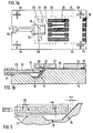
- FIG. 1 shows a proposed signal conversion arrangement in plan view and in longitudinal section
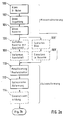
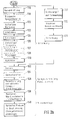
- Figure 2 a Flow chart of the proposed manufacturing process
- Figure 3 shows a detail of a mold
- Figure 4 shows a Cross section through an embossed V-groove before and after Sintering
- Figure 5 shows a longitudinal section through an embossed Microstructure with optical fiber to illustrate the Effects of shrinkage during sintering
- Figure 6 a Illustration of the use of a press tool in Sintering
- Figure 7 shows a transducer arrangement with an ellipsoidal mirror.
- the reflection preferably takes place at an angle of 90 degrees, the mirror 15 then has an inclination to the optical axis of the optical fiber 20 of 45 degrees.
- a receiver or a transmitter 22 and an RF (radio frequency) preamplifier 24 are arranged on the top 19 of the ceramic substrate 10. Both elements 22, 24 are preferably designed in the form of chips. They are connected to the ceramic substrate 10 via contact surfaces 29, which also serve for fixing. Transmitter / receiver chip 22 and RF preamplifier 24 are connected to one another via conductor tracks 26 which are also applied to the surface 19 of the ceramic substrate 10 and which are all or partially designed as strip conductors. Further strip conductors 26 ', applied directly to the ceramic substrate 10 in the same way, serve to integrate the entire transducer arrangement into the surrounding electronics.
- the transmitter / receiver chip 22 has a detection window 28 on its underside, ie on the side facing the substrate surface 19. It is located exactly above the beam spot, which generates the light transmitted via the optical fiber 20 and reflected on the mirror 15.
- the detection window 28 is generally a photodiode, which receives light transmitted via the optical fiber 20.
- the window 28 is, for example, a surface-emitting laser diode which feeds light into the optical fiber 20 via the mirror 15.
- An essential advantage of the arrangement shown in FIG. 1 is the use of a ceramic substrate 10. This means that additional insulation of the conductor tracks 26 and contact surfaces 25 from the surface 19 of the substrate 10 can be omitted. This in turn also allows the steps of mirror production and metallization of the conductor tracks or contact areas 25 to be combined.
- Figure 2 illustrates with the aid of a flow chart Sequence of a for producing an arrangement according to FIG. 1 appropriate procedure. It is divided into the sub-processes Microstructuring, electroforming, molding, Mirror production and metallization, as well as micro assembly.
- the first process sub-process is used to produce a Master structure for the impression. This is expediently done by known microtechnologies, for example in silicon micromechanics.
- a silicon waver in one first step 100 in a known manner, preferably by means of an anisotropic etching process in hot KOH solution, V-grooves 11 ', which will later be used as management structures for the Optical fibers 20 serve. Your depth can, as the Walls of the V-grooves along the (111-) crystal faces in the Always form silicon under a slope of 54.7 degrees, in simple way through the opening width of the Lithography mask can be determined.
- the experimental Accuracy is about 1 ⁇ m.
- step 102 one as Depression serving recess 13 etched. Your measurements depend on the diameter of the optical fiber 20 surrounding protective jacket 21. Am inside the silicon wafer 10 'lying end of the V-groove is then in step 104 trough-shaped cavern 12 'etched.
- FIG. 3 shows Illustration of the process flow a detail of a Master structure with V-groove 11 'and cavern 12'. In the structures for train interception, Fiber guidance and mirror in a single mask process defined and etched together.
- a practical one Possibility to create any inclination of the Mirror 15, for example 45 degrees, provides that Cavern 12 'initially with a contour material 16, in simple way to fill up a plastic, step 106, which is then stamped under the the desired angle of the ground cutting edge is formed, Step 108. Thereby possibly got into the V-groove 11 ' Plastic residues can be removed, for example, by laser ablation be selectively removed.
- Another, also useful Possibility to generate a mirror 15 with any Mirror surface provides the desired mirror contour For example, grind in a Pyrex glass and this in to insert the cavern 12 ', step 108'.
- the is fixed Glass bodies are expedient by direct bonding with the silicon.
- the prepared silicon master structure is metallized, Step 110, followed by electroplating a metal mold in a manner known per se produced.
- a metal mold in a manner known per se produced.
- This can be done by passivating the electroplating surface and then electroplating is grown on electroplating.
- the first mold insert the so-called mother, is created here an intermediate copy as the first generation, of which in turn by taking a second mold Generation. Since many interim copies of a mother and of each intermediate copy, many form inserts of the second Generation can be demolded inexpensively is one cost effective multiplication of molds easily possible.
- the impression with the help of Molding tools made of ceramic substrates 10 ', which The basis of the arrangement according to Figure 1 are.
- Cast ceramic green tapes are the starting material in foil form. They consist of compounds in particular fine-grained ceramic powder with organic binders, their Thicknesses typically range between 100 and 800 ⁇ m.
- the Impression molding process a pre-compression of the ceramic films by pressing. The measure will Structural fidelity improved in the later sintering process. To one sufficiently smooth surface of the later mirror 15 can then ensure on the for the mirror 15 intended area, i.e.
- one smooth sintered glass paste can be printed locally, step 118.
- step 120 the molding tool is moved to the in prepared steps 116 and 118 placed film.
- the film, and optionally also the molding tool, is now heated, step 122, then the mold is in embossed the film, step 124. This is followed by Cooling the film with constant holding pressure, step 130 as well as the demolding.
- Step 132 the embossed foils are compacted.
- Steps 116 through 130 may take the impression more advantageously Way also by casting (slip casting) of liquid ceramic slip on a molding tool, step 117. Of the Ceramic slip is then dried, step 119, demolded from the mold, step 121, and again sintered, step 132.
- the slip casting process draws is characterized by a very even material compression. This can cause uneven shrinkage in the subsequent Sintering process are largely prevented.
- an isotropic occurs during sintering Shrinkage typically around 20%.
- careful Control of the sintering process in step 132 i.e. in particular by closely monitoring the temperatures and the sintering time, as well as by appropriate coordination of Embossing parameters, powder quality and sintering parameters but is a reproducibility of the structure shown possible with an accuracy of ⁇ 1% of the shrinkage.
- shrinkage can occur during the manufacture of the Master structures are kept in the first sub-process.
- FIG. 4 illustrates the influence of shrinkage when sintering using the shrinkage of a V-groove.
- step 132 leads easily alongside Rounding of corners and edges, as in Figure 4 indicated.
- Sidewalls are adjusting while the trench tip the V-structure and the upper edges are not can have a determining effect on the problem of Rounding through a suitable design of the microstructures be counteracted well. This applies in particular to the mirror surfaces, because for the function of the mirror 15 as Deflection element also only the inclined surface essential is, but not the bounding edges.
- the main consequence of the shrinkage is, as in FIG. 5 shown, a height shift of the optical axis of the Optical fiber 20 by an amount ⁇ h.
- a height shift of the optical axis of the Optical fiber 20 by an amount ⁇ h is particularly easy.
- the effects of the shrinkage can be controlled, if, as assumed in Figure 5, a less than 45 degrees against the optical axis of the optical fiber inclined mirror 15 is used. This reflects over the optical fiber 20 transmitted light always vertically upwards.
- the through the beam spot caused by the light moves due to this the shrinkage by an amount ⁇ x in the direction of the optical Axis of the optical fiber 20, which with the Height shift ⁇ h of the optical fiber 20 matches.
- a pressing tool 23 is placed on the embossed ceramic substrate 10 during the sintering. It consists of a refractory material, for example of silicon nitride (Si 3 N 4 ) or aluminum oxide (Al 2 O 3 ) and is coated on the contact surface to the ceramic substrate 10 with a release agent 17. The latter can also be applied to the ceramic substrate 10.
- the surface of the pressing tool 23 corresponds to an exact negative impression of the embossed surface of the ceramic substrate 10. With the help of the pressing tool 10, a pressure P is now exerted on the ceramic substrate 10 during the sintering. If the pressure P is sufficient, shrinkage of the ceramic substrate 10 can be almost completely avoided, and the structures produced during embossing remain true to size.
- the pressing tool 23 is expediently designed to be slightly porous, so that the exhaust gases generated during the sintering fire through the Press tool 23 can escape.
- a release agent 17 is in usually required to press tool 23 and Ceramic substrate 10 from each other again after sintering to be able to separate.
- a single tool both as a molding tool for performing steps 117 or 124 as well as a pressing tool for use be provided in the manner described above. This is particularly useful if the impression is taken Ceramic slip casting according to steps 117 to 121 he follows.
- the mold can already be used a release agent 17 may be coated so that a Demolding, step 121 before sintering, step 132 can be omitted.
- step 124 also a two stage Embossing may be provided.
- the film is thereby in step 124 first embossed with reduced embossing pressure.
- the mold is raised and on smooth sintering material, preferably a Glass ceramic material, filled into the structure produced, Step 126. If necessary, the material is predried, Step 127. This is followed by a second embossing step, Step 128 the final impression.
- mirror smoothing in the form of a selective coating the surface provided for the mirror 15 take place to Example by spray coating, with a polymer film, such as such as photoresist, polyimide, or benzocyclobutene.
- a polymer film such as such as photoresist, polyimide, or benzocyclobutene.
- Such a Polymer film smoothes the coated surface directly or if necessary after melting once.
- Another smoothing of the Mirror surface can be created by glossy galvanic Strengthening of the metallization can be achieved.
- the electrical wiring which is usually a High frequency wiring in the form of coplanar Includes strip conductors, as well as the contact surfaces 29 (Contact pads) for connecting the electrical components 22, 24 applied.
- the metallization of the masking step is expedient Mirror surface.
- the mask is embossed on the Alignment marks 18 aligned, thus lateral shrinkage automatically taken into account in the position of the electrodes.
- the metallized ceramic substrate 10 is final populated, step 140.
- the transmitter / receiver chip 22 on the prepared one Contact surfaces 29 placed and connected to the substrate (bonded).
- About the melting solder balls on the Contact pads 29 is in a manner known per se Self-centering possible.
- an active adjustment of the transmitter / receiver chip with an optical Positioning device take place.
- Receiver diode with the detection zone up over the Mirrors 15 are mounted when the wafer material for the light wavelength to be received is transparent.
- the preamplifier tip 24 is applied in this manner. After that the optical fiber 20 is placed in the fiber-guiding V-groove 11, pushed under the chip 22 to the mirror 15 and fixed.
- the signals are usually transmitted via the converter arrangement described at a transmission rate of 5 to 11 gigabits / second.
- the active area of the diode 28 must therefore not exceed a diameter of approximately 50 ⁇ m in order to be able to keep the diode capacitances small.
- a smaller beam spot is created by filling a medium with a larger refractive index into the cavern 12 reached, step 140.
- the Beam spot by inserting an optical epoxy adhesive with a refractive index of typically n ⁇ 1.5 to about Reduce 20 ⁇ m. This is a high bit rate Receiver module possible without further beam focusing.
- the mirror 15 can for this purpose, for example, be designed as a concave mirror.
- While maintaining the underlying concepts is one Variety of configurations of the previously described Arrangement or the procedure possible. That's how it is Manufacturing process not based on a ceramic stamping technique limited. Rather, it is similarly expandable to others moldable materials such as thermoplastic Plastics, reaction casting resins, slip casting, sprayable Ceramic compounds or organically modified ceramics. Basically, the procedure is not based on that either Manufacture of electro-optical converter arrangements restricted, but also allows, for example, the Manufacture of micro-optical benches.
- fiber guides in the form of V-grooves Mounts for other micro-optical components, such as optical isolators, microlenses, filter pads, etc. embossed.
Landscapes
- Physics & Mathematics (AREA)
- General Physics & Mathematics (AREA)
- Optics & Photonics (AREA)
- Optical Couplings Of Light Guides (AREA)
- Mechanical Coupling Of Light Guides (AREA)
Abstract
Claims (24)
- Procédé de fabrication d'un dispositif pour convertir des signaux optiques en signaux électriques, comprenant un substrat avec des structures pour guider une fibre optique et dévier la lumière transmise par la fibre optique, les structures (11, 12, 13) étant réalisées sur le substrat (10) par fabrication d'une pièce moulée sur le contour d'un moule,
caractérisé en ce que
pour le substrat (10) on utilise une matière de base céramique et on moule par matriçage ou coulée d'une matière céramique de base. - Procédé selon la revendication 1,
caractérisé en ce que
le moulage se fait par coulée de barbotine de céramique sur un outil de moulage. - Procédé selon la revendication 1,
caractérisé en ce que
le moulage se fait par matriçage par projection, injection ou coulée avec réaction. - Procédé selon la revendication 1,
caractérisé en ce que
la matière première du substrat (10) est une feuille comportant la matière de base céramique. - Procédé selon la revendication 1,
caractérisé en ce que
le substrat en céramique (10) est fritté après matriçage ou coulée (130). - Procédé selon la revendication 4,
caractérisé en ce que
la feuille est un composé de poudre de céramique à grains fins et d'un liant organique constituant un ruban construit. - Procédé selon la revendication 4,
caractérisé en ce qu'
on réalise les structures sur la feuille de substrat selon les étapes suivantes :a) mise en place d'un outil de moulage sur la feuille,b) chauffage de la feuille,c) impression de l'outil de moulage dans la feuille,d) refroidissement de la feuille. - Procédé selon la revendication 4,
caractérisé en ce qu'
on précomprime la feuille de substrat en surface (116) avant d'imprimer l'outil de moulage. - Procédé selon la revendication 5,
caractérisé en ce qu'
on met le substrat (10) en pression pendant le frittage à l'aide d'un outil de pressage (23). - Procédé selon la revendication 9,
caractérisé en ce qu'
on applique un agent séparateur (17) entre l'outil de pressage (23) et le substrat (10). - Procédé selon la revendication 9,
caractérisé en ce que
l'outil de pressage (23) est une matière poreuse. - Procédé selon la revendication 9,
caractérisé en ce que
l'outil de pressage (23) est l'outil de moulage utilisé pour fabriquer les structures (11, 12, 13) dans le substrat (10). - Procédé selon la revendication 1,
caractérisé en ce qu'
on applique une pâte de verre lisse par frittage (126) sur le substrat (10) avant de le matricer. - Procédé selon la revendication 1,
caractérisé en ce qu'
on effectue tout d'abord une première étape de matriçage (124) avec une pression de matriçage réduite sur la micro-structure obtenue puis, on applique une matière lisse par frittage (126) puis on effectue une seconde étape de matriçage (128) pour réaliser la structure définitive. - Procédé selon la revendication 1,
caractérisé en ce qu'
on effectue un préséchage de la structure après application de la matière lisse par frittage. - Procédé selon la revendication 1,
caractérisé en ce que
sur le substrat structuré (10), on applique au cours d'une même étape de masquage (136), les chemins conducteurs (26) et des surfaces de contact (29) et on métallise la structure de déviation de la lumière (15). - Procédé selon la revendication 1,
caractérisé en ce que
la structure de déviation de la lumière (15) est en forme de miroir et la surface prévue à cet effet est tout d'abord lissée puis métallisée. - Procédé selon la revendication 1,
caractérisé en ce que
la structure de renvoi de la lumière (15) est en forme de miroir et la surface prévue pour cela reçoit tout d'abord une métallisation de base puis on renforce par une application galvanique améliorant la planéité ou renforçant la brillance. - Procédé selon la revendication 1,
caractérisé en ce que
la zone (12) de la structure servant à guider la fibre optique, à l'endroit où se trouve l'orifice de sortie (27) d'une fibre optique (20) placée dans la structure de guidage (11, 12, 13) est remplie d'une matière dont l'indice de réfraction est supérieur à 1. - Dispositif pour convertir des signaux optiques en signaux électriques comprenant un substrat dont la face supérieure comporte des structures pour guider une fibre optique et des moyens pour dévier la lumière transmise par la fibre optique sur un convertisseur placé sur le substrat pour convertir les signaux optiques en signaux électriques,
caractérisé en ce que
le substrat (10) est formé d'une matière de base céramique isolante électrique et le moyen de déviation de la lumière (15) est également formé sur la surface du substrat (10). - Dispositif selon la revendication 20,
caractérisé en ce que
la face supérieure (19) du substrat (10) comporte des chemins conducteurs (26, 26') pour transmettre les signaux électriques du convertisseur (22). - Dispositif selon la revendication 20,
caractérisé en ce que
les moyens pour dévier la lumière transmise par la fibre optique sont constitués par un miroir (15) à contour librement prédétermine. - Dispositif selon la revendication 20,
caractérisé en ce qu'
entre l'orifice de sortie de la fibre optique (27) et l'entrée (28) du convertisseur (22) on place une matière ayant un indice de réfraction supérieur à celui de l'air. - Dispositif selon la revendication 20,
caractérisé en ce qu'
à la place de la diode de réception, on utilise une diode laser à émission de surface dont la lumière est injectée dans la fibre optique par l'intermédiaire de l'élément déviateur.
Applications Claiming Priority (5)
| Application Number | Priority Date | Filing Date | Title |
|---|---|---|---|
| DE19501285A DE19501285C1 (de) | 1995-01-18 | 1995-01-18 | Anordnung zur Umsetzung von optischen in elektrische Signale und Verfahren zur Herstellung |
| DE19501285 | 1995-01-18 | ||
| DE19547941A DE19547941A1 (de) | 1995-01-18 | 1995-12-21 | Anordnung zur Umsetzung von optischen in elektrische Signale und Verfahren zur Herstellung |
| DE19547941 | 1995-12-21 | ||
| PCT/DE1996/000026 WO1996022177A1 (fr) | 1995-01-18 | 1996-01-10 | Systeme permettant de convertir des signaux optiques en signaux electriques et procede de production |
Publications (2)
| Publication Number | Publication Date |
|---|---|
| EP0804323A1 EP0804323A1 (fr) | 1997-11-05 |
| EP0804323B1 true EP0804323B1 (fr) | 1998-11-04 |
Family
ID=26011677
Family Applications (1)
| Application Number | Title | Priority Date | Filing Date |
|---|---|---|---|
| EP96900267A Expired - Lifetime EP0804323B1 (fr) | 1995-01-18 | 1996-01-10 | Systeme permettant de convertir des signaux optiques en signaux electriques et procede de production |
Country Status (3)
| Country | Link |
|---|---|
| US (1) | US5987202A (fr) |
| EP (1) | EP0804323B1 (fr) |
| WO (1) | WO1996022177A1 (fr) |
Families Citing this family (71)
| Publication number | Priority date | Publication date | Assignee | Title |
|---|---|---|---|---|
| JP3677348B2 (ja) * | 1996-05-24 | 2005-07-27 | 株式会社リコー | 光伝送モジュール |
| JP2907203B1 (ja) | 1998-02-20 | 1999-06-21 | 住友電気工業株式会社 | 光モジュール |
| US6115521A (en) * | 1998-05-07 | 2000-09-05 | Trw Inc. | Fiber/waveguide-mirror-lens alignment device |
| DE69907351T2 (de) | 1998-09-18 | 2003-11-06 | Sumitomo Electric Industries, Ltd. | Photodiodenmodul |
| DE19861162A1 (de) | 1998-11-06 | 2000-06-29 | Harting Elektrooptische Bauteile Gmbh & Co Kg | Verfahren zur Herstellung einer Leiterplatte sowie Leiterplatte |
| TW460717B (en) * | 1999-03-30 | 2001-10-21 | Toppan Printing Co Ltd | Optical wiring layer, optoelectric wiring substrate mounted substrate, and methods for manufacturing the same |
| JP2001174671A (ja) * | 1999-12-16 | 2001-06-29 | Japan Aviation Electronics Industry Ltd | 光素子モジュール |
| DE10001679C2 (de) * | 2000-01-12 | 2001-11-29 | Infineon Technologies Ag | Optische Kopplungsanordnung |
| DE20013088U1 (de) * | 2000-07-28 | 2000-11-16 | Harting Elektro-optische Bauteile GmbH & Co. KG, 31162 Bad Salzdetfurth | Optischer Transceiver |
| DE10043985A1 (de) * | 2000-09-05 | 2002-03-14 | Cube Optics Ag | Optischer Modifizierer und Verfahren zur Herstellung hierfür |
| DE10043996A1 (de) * | 2000-09-05 | 2002-03-14 | Cube Optics Ag | Koppelvorrichtung und Verfahren zur Herstellung hierfür |
| TW449797B (en) * | 2000-09-22 | 2001-08-11 | Ind Tech Res Inst | Integrated surface-emitting type electro-optical module and the fabrication method thereof |
| US6905260B2 (en) | 2000-12-26 | 2005-06-14 | Emcore Corporation | Method and apparatus for coupling optical elements to optoelectronic devices for manufacturing optical transceiver modules |
| US7021836B2 (en) | 2000-12-26 | 2006-04-04 | Emcore Corporation | Attenuator and conditioner |
| US6867377B2 (en) | 2000-12-26 | 2005-03-15 | Emcore Corporation | Apparatus and method of using flexible printed circuit board in optical transceiver device |
| US6863444B2 (en) | 2000-12-26 | 2005-03-08 | Emcore Corporation | Housing and mounting structure |
| US6799902B2 (en) | 2000-12-26 | 2004-10-05 | Emcore Corporation | Optoelectronic mounting structure |
| DE10065624C2 (de) * | 2000-12-29 | 2002-11-14 | Hans Kragl | Kopplungsanordnung zum optischen Koppeln eines Lichtwellenleiters mit einem elektro-optischen oder opto-elektrischen Halbleiterwandler |
| GB2372108A (en) * | 2001-02-10 | 2002-08-14 | Bookham Technology Plc | Alignment of optical component using V-grooves in an optical chip |
| US6786651B2 (en) * | 2001-03-22 | 2004-09-07 | Primarion, Inc. | Optical interconnect structure, system and transceiver including the structure, and method of forming the same |
| WO2002077691A2 (fr) * | 2001-03-22 | 2002-10-03 | Primarion, Inc. | Structure d'interconnexion optique, systeme et emetteur-recepteur renfermant cette structure, et procede de fabrication associe |
| US20020195417A1 (en) * | 2001-04-20 | 2002-12-26 | Steinberg Dan A. | Wet and dry etching process on <110> silicon and resulting structures |
| US6704488B2 (en) * | 2001-10-01 | 2004-03-09 | Guy P. Lavallee | Optical, optoelectronic and electronic packaging platform, module using the platform, and methods for producing the platform and the module |
| US6934430B2 (en) * | 2002-02-04 | 2005-08-23 | Telephus Inc. | Optical module used in high frequency band optical communication system |
| US6688780B2 (en) | 2002-02-07 | 2004-02-10 | Amphenol Corporation | Cantilevered shutter for optical adapter |
| JP3833180B2 (ja) * | 2002-02-08 | 2006-10-11 | キヤノン株式会社 | 二次元光導波路の製造方法 |
| FR2836236B1 (fr) * | 2002-02-21 | 2004-09-17 | Framatome Connectors Int | Dispositif de couplage optoelectronique perfectionne |
| JP2006506657A (ja) * | 2002-03-14 | 2006-02-23 | エスエーイー・マグネティクス(エイチ・ケイ)リミテッド | 光ファイバーとの半導体装置の能動的光学整合のための一体化プラットホーム |
| US20040021214A1 (en) * | 2002-04-16 | 2004-02-05 | Avner Badehi | Electro-optic integrated circuits with connectors and methods for the production thereof |
| EP1502135A2 (fr) * | 2002-04-16 | 2005-02-02 | Xloom Photonics Ltd. | Circuits optoelectroniques presentant un connecteur et leurs procedes de production |
| US7180929B2 (en) * | 2002-04-18 | 2007-02-20 | Intel Corporation | Wafer-level test structure for edge-emitting semiconductor lasers |
| US6657272B2 (en) * | 2002-04-19 | 2003-12-02 | Triquint Technology Holding Co. | Off-axis silicon substrate for optimized optical coupling |
| GB2387714A (en) * | 2002-04-19 | 2003-10-22 | Denselight Semiconductors Pte | Mount for a semiconductor device |
| CA2484349A1 (fr) * | 2002-05-09 | 2003-11-20 | Sumitomo Electric Industries, Ltd. | Dispositif optique |
| JP2004088046A (ja) * | 2002-06-25 | 2004-03-18 | Sumitomo Electric Ind Ltd | 光受信器及びその製造方法 |
| US6863453B2 (en) | 2003-01-28 | 2005-03-08 | Emcore Corporation | Method and apparatus for parallel optical transceiver module assembly |
| US7150569B2 (en) * | 2003-02-24 | 2006-12-19 | Nor Spark Plug Co., Ltd. | Optical device mounted substrate assembly |
| US7343058B2 (en) * | 2003-04-22 | 2008-03-11 | Intel Corporation | Efficient light coupler from off-chip to on-chip waveguides |
| CN100365775C (zh) * | 2003-05-23 | 2008-01-30 | 罗姆和哈斯电子材料有限责任公司 | 用于显微机械加工晶体材料的蚀刻方法以及由此方法制备的器件 |
| US6898347B2 (en) * | 2003-05-30 | 2005-05-24 | Intel Corporation | Monitoring power in optical networks |
| AU2003272062A1 (en) * | 2003-10-15 | 2005-04-27 | Xloom Photonics Ltd. | Electro-optical circuitry having integrated connector and methods for the production thereof |
| DE60321583D1 (de) * | 2003-12-24 | 2008-07-24 | St Microelectronics Srl | Optisches Modul mit einer optoelektronischen Einrichtung und einer reflektierenden optischen Kupplungsvorrichtung |
| US7369718B2 (en) * | 2004-01-23 | 2008-05-06 | Intel Corporation | Package substrate pattern to accommodate optical waveguide |
| US7306378B2 (en) * | 2004-05-06 | 2007-12-11 | Intel Corporation | Method and apparatus providing an electrical-optical coupler |
| US7782921B2 (en) * | 2005-03-28 | 2010-08-24 | Intel Corporation | Integrated optical detector in semiconductor reflector |
| EP1715368B1 (fr) * | 2005-04-18 | 2008-04-09 | Varioprint AG | Procédé de fabrication d'un dispositif de couplage optique |
| KR100749528B1 (ko) * | 2005-09-30 | 2007-08-16 | 주식회사 두산 | 광 접속 모듈 및 그 제조 방법 |
| US7450621B1 (en) * | 2007-06-26 | 2008-11-11 | Avago Technologies Fiber Ip (Singapore) Pte. Ltd. | Integrated laser-diffractive lens device |
| US20090093137A1 (en) * | 2007-10-08 | 2009-04-09 | Xloom Communications, (Israel) Ltd. | Optical communications module |
| US8173045B2 (en) | 2008-05-28 | 2012-05-08 | University Of Washington | Diels-Alder crosslinkable dendritic nonlinear optic chromophores and polymer composites |
| US7703993B1 (en) | 2008-12-17 | 2010-04-27 | National Semiconductor Corporation | Wafer level optoelectronic package with fiber side insertion |
| US9151918B2 (en) * | 2010-08-26 | 2015-10-06 | Vi Systems Gmbh | Opto-electronic assembly for parallel high speed transmission |
| EP2434321A1 (fr) * | 2010-09-27 | 2012-03-28 | U2t Photonics Ag | Module optique |
| US8582618B2 (en) | 2011-01-18 | 2013-11-12 | Avago Technologies General Ip (Singapore) Pte. Ltd. | Surface-emitting semiconductor laser device in which an edge-emitting laser is integrated with a diffractive or refractive lens on the semiconductor laser device |
| US8818144B2 (en) | 2011-01-25 | 2014-08-26 | Tyco Electronics Corporation | Process for preparing an optical interposer for waveguides |
| AT12749U1 (de) * | 2011-04-01 | 2012-10-15 | Austria Tech & System Tech | Leiterplattenelement mit wenigstens einer led |
| US8315287B1 (en) | 2011-05-03 | 2012-11-20 | Avago Technologies Fiber Ip (Singapore) Pte. Ltd | Surface-emitting semiconductor laser device in which an edge-emitting laser is integrated with a diffractive lens, and a method for making the device |
| US9052460B2 (en) * | 2011-12-27 | 2015-06-09 | Neophotonics Corporation | Integrated circuit coupling system with waveguide circuitry and method of manufacture thereof |
| US8757897B2 (en) * | 2012-01-10 | 2014-06-24 | Invensas Corporation | Optical interposer |
| US9323010B2 (en) | 2012-01-10 | 2016-04-26 | Invensas Corporation | Structures formed using monocrystalline silicon and/or other materials for optical and other applications |
| US9054024B2 (en) * | 2012-02-13 | 2015-06-09 | Futurewei Technologies, Inc. | Apparatus and method for optical communications |
| US9618712B2 (en) | 2012-02-23 | 2017-04-11 | Taiwan Semiconductor Manufacturing Company, Ltd. | Optical bench on substrate and method of making the same |
| US10180547B2 (en) | 2012-02-23 | 2019-01-15 | Taiwan Semiconductor Manufacturing Company, Ltd. | Optical bench on substrate |
| US20160377821A1 (en) | 2012-03-05 | 2016-12-29 | Nanoprecision Products, Inc. | Optical connection of optical fibers to grating couplers |
| US9323014B2 (en) * | 2012-05-28 | 2016-04-26 | Mellanox Technologies Ltd. | High-speed optical module with flexible printed circuit board |
| US20130330033A1 (en) * | 2012-06-12 | 2013-12-12 | Futurewei Technologies, Inc. | Tsv substrate with mirror and its application in high-speed optoelectronic packaging |
| US20150331212A1 (en) * | 2013-01-31 | 2015-11-19 | Ccs Technology, Inc. | Method for forming optoelectronic modules connectable to optical fibers and optoelectronic module connectable to at least one optical fiber |
| JP6286853B2 (ja) * | 2013-04-04 | 2018-03-07 | 富士通株式会社 | 電子装置とその製造方法、及び電子機器 |
| US10151865B2 (en) * | 2014-05-02 | 2018-12-11 | Futurewei Technologies, Inc. | Compact external grating PBS/PBC coupler |
| US20170119250A1 (en) * | 2015-11-04 | 2017-05-04 | The Charles Stark Draper Laboratory, Inc. | Portable hardware fixture for fundoscopy |
| RU2670719C9 (ru) * | 2018-02-05 | 2018-11-29 | Российская Федерация, от имени которой выступает ФОНД ПЕРСПЕКТИВНЫХ ИССЛЕДОВАНИЙ | Оптоволоконный фотоэлектрический свч модуль |
Family Cites Families (14)
| Publication number | Priority date | Publication date | Assignee | Title |
|---|---|---|---|---|
| US4169001A (en) * | 1976-10-18 | 1979-09-25 | International Business Machines Corporation | Method of making multilayer module having optical channels therein |
| US4445274A (en) * | 1977-12-23 | 1984-05-01 | Ngk Insulators, Ltd. | Method of manufacturing a ceramic structural body |
| US4546065A (en) * | 1983-08-08 | 1985-10-08 | International Business Machines Corporation | Process for forming a pattern of metallurgy on the top of a ceramic substrate |
| GB2162335B (en) * | 1984-07-25 | 1988-07-13 | Adc Telecommunications Inc | Fibre optic coupler |
| DE3543558C2 (de) * | 1985-12-10 | 1996-09-19 | Licentia Gmbh | Opto-elektrische Koppelanordnung |
| US4897711A (en) * | 1988-03-03 | 1990-01-30 | American Telephone And Telegraph Company | Subassembly for optoelectronic devices |
| DE4106721A1 (de) * | 1991-03-02 | 1992-09-10 | Ant Nachrichtentech | Anordnung zur ankopplung von lichtwellenleiterenden an empfangselemente |
| DE4212208A1 (de) * | 1992-04-10 | 1993-10-14 | Bosch Gmbh Robert | Verfahren zur Herstellung optischer Polymerbauelemente mit integrierter Faser-Chip-Kopplung in Abformtechnik |
| DE4300652C1 (de) * | 1993-01-13 | 1994-03-31 | Bosch Gmbh Robert | Verfahren zur Herstellung einer hybrid integrierten optischen Schaltung und Vorrichtung zur Emission von Lichtwellen |
| JP3484543B2 (ja) * | 1993-03-24 | 2004-01-06 | 富士通株式会社 | 光結合部材の製造方法及び光装置 |
| DE4317953A1 (de) * | 1993-05-28 | 1994-12-01 | Siemens Ag | Verfahren zur Herstellung von Führungselementen für Lichtwellenleiter |
| CA2130738A1 (fr) * | 1993-11-01 | 1995-05-02 | Keith Wayne Goossen | Methode et dispositif de fabrication de miroirs a inclinaison quelconque dans les substrats pour les systemes optiques hybrides |
| EP0660146B1 (fr) * | 1993-12-27 | 2002-10-09 | Nec Corporation | Structure récepteur de lumière pour dispositifs optiques du type guide d'ondes |
| JP3828179B2 (ja) * | 1995-05-12 | 2006-10-04 | 富士通株式会社 | 半導体光検出装置およびその製造方法 |
-
1996
- 1996-01-10 EP EP96900267A patent/EP0804323B1/fr not_active Expired - Lifetime
- 1996-01-10 US US08/875,263 patent/US5987202A/en not_active Expired - Fee Related
- 1996-01-10 WO PCT/DE1996/000026 patent/WO1996022177A1/fr not_active Ceased
Also Published As
| Publication number | Publication date |
|---|---|
| US5987202A (en) | 1999-11-16 |
| EP0804323A1 (fr) | 1997-11-05 |
| WO1996022177A1 (fr) | 1996-07-25 |
Similar Documents
| Publication | Publication Date | Title |
|---|---|---|
| EP0804323A1 (fr) | Systeme permettant de convertir des signaux optiques en signaux electriques et procede de production | |
| EP0614539B1 (fr) | Procede de fabrication d'un couvercle pour un circuit optique integre | |
| EP0635139B1 (fr) | Procede pour la fabrication de composants optiques en polymere avec couplage integre puce/fibre par moulage | |
| EP0630486B1 (fr) | Procede de fabrication d'un circuit optique integre de maniere hybride et dispositif permettant d'emettre des ondes lumineuses | |
| DE60301553T2 (de) | Optischer schaltkreis mit optischen planaren hohlkern-lichtwellenleitern | |
| EP0647328B1 (fr) | Element polymere optique pour coupler des cellules photo-electriques a des circuits optiques integres | |
| DE69907351T2 (de) | Photodiodenmodul | |
| DE19619353A1 (de) | Verfahren zur Herstellung eines integriert optischen Wellenleiterbauteiles sowie Anordnung | |
| WO2003019617A2 (fr) | Procede de production de composants electroniques | |
| DE10023736A1 (de) | Leiterplatte sowie Verfahren zur Herstellung einer Leiterplatte | |
| DE19623153B4 (de) | Optokoppler und Verfahren zur Herstellung desselben | |
| DE112006000228T5 (de) | Optokoppler | |
| DE19501285C1 (de) | Anordnung zur Umsetzung von optischen in elektrische Signale und Verfahren zur Herstellung | |
| EP0429877B1 (fr) | Dispositif de positionnement de fibres optiques dans des éléments de connexion | |
| EP0883825B1 (fr) | Procede de production de composants optiques avec guides d'ondes optiques accouples, et composants optiques produits selon ce procede | |
| DE4240950C1 (de) | Verfahren zum Herstellen eines Deckels für eine integriert optische Schaltung und Deckel für eine integriert optische Schaltung | |
| EP0731365B1 (fr) | Méthode de fabrication d'un dispositif électro-optique | |
| DE19616015C1 (de) | Anordnung zur Ankopplung optischer Sende- oder Empfangselemente an einen Lichtwellenleiter | |
| EP1671167B1 (fr) | Procede de realisation de cartes de circuits imprimes electro-optiques comprenant des guides d'onde polysiloxane, et leur utilisation | |
| DE10200853B4 (de) | Optische Lage mit optischen Leitern, Leiterplatte, Herstellungsverfahren für optische Lage mit optischen Leitern und Herstellungsverfahren für Leiterplatte | |
| DE10132794A1 (de) | Kopplung an in Leiterplatten eingebettete Lichtleiter | |
| EP1005663A1 (fr) | Procede de production d'un composant optique integre a la puce a guides d'ondes avec connecteur enfichable | |
| DE10222960A1 (de) | Verfahren zur Herstellung von elektronischen Bauelementen | |
| DE19521170A1 (de) | Verfahren zum Herstellen von grabenförmigen Strukturen in integriert-optischen Bauelementen | |
| EP0692724A1 (fr) | Procédé pour la fabrication et l'alignement d'un dispositif à semi-conducteur |
Legal Events
| Date | Code | Title | Description |
|---|---|---|---|
| PUAI | Public reference made under article 153(3) epc to a published international application that has entered the european phase |
Free format text: ORIGINAL CODE: 0009012 |
|
| 17P | Request for examination filed |
Effective date: 19970818 |
|
| AK | Designated contracting states |
Kind code of ref document: A1 Designated state(s): CH DE FR GB IT LI SE |
|
| GRAG | Despatch of communication of intention to grant |
Free format text: ORIGINAL CODE: EPIDOS AGRA |
|
| 17Q | First examination report despatched |
Effective date: 19980116 |
|
| GRAG | Despatch of communication of intention to grant |
Free format text: ORIGINAL CODE: EPIDOS AGRA |
|
| GRAH | Despatch of communication of intention to grant a patent |
Free format text: ORIGINAL CODE: EPIDOS IGRA |
|
| GRAH | Despatch of communication of intention to grant a patent |
Free format text: ORIGINAL CODE: EPIDOS IGRA |
|
| GRAA | (expected) grant |
Free format text: ORIGINAL CODE: 0009210 |
|
| AK | Designated contracting states |
Kind code of ref document: B1 Designated state(s): CH DE FR GB IT LI SE |
|
| REG | Reference to a national code |
Ref country code: CH Ref legal event code: NV Representative=s name: SCINTILLA AG, DIREKTION Ref country code: CH Ref legal event code: EP |
|
| REF | Corresponds to: |
Ref document number: 59600776 Country of ref document: DE Date of ref document: 19981210 |
|
| ITF | It: translation for a ep patent filed | ||
| GBT | Gb: translation of ep patent filed (gb section 77(6)(a)/1977) |
Effective date: 19990112 |
|
| ET | Fr: translation filed | ||
| PLBE | No opposition filed within time limit |
Free format text: ORIGINAL CODE: 0009261 |
|
| STAA | Information on the status of an ep patent application or granted ep patent |
Free format text: STATUS: NO OPPOSITION FILED WITHIN TIME LIMIT |
|
| 26N | No opposition filed | ||
| REG | Reference to a national code |
Ref country code: GB Ref legal event code: IF02 |
|
| PGFP | Annual fee paid to national office [announced via postgrant information from national office to epo] |
Ref country code: GB Payment date: 20021218 Year of fee payment: 8 |
|
| PGFP | Annual fee paid to national office [announced via postgrant information from national office to epo] |
Ref country code: FR Payment date: 20030117 Year of fee payment: 8 |
|
| PGFP | Annual fee paid to national office [announced via postgrant information from national office to epo] |
Ref country code: SE Payment date: 20030123 Year of fee payment: 8 |
|
| PGFP | Annual fee paid to national office [announced via postgrant information from national office to epo] |
Ref country code: CH Payment date: 20030124 Year of fee payment: 8 |
|
| PGFP | Annual fee paid to national office [announced via postgrant information from national office to epo] |
Ref country code: DE Payment date: 20030225 Year of fee payment: 8 |
|
| PG25 | Lapsed in a contracting state [announced via postgrant information from national office to epo] |
Ref country code: GB Free format text: LAPSE BECAUSE OF NON-PAYMENT OF DUE FEES Effective date: 20040110 |
|
| PG25 | Lapsed in a contracting state [announced via postgrant information from national office to epo] |
Ref country code: SE Free format text: LAPSE BECAUSE OF NON-PAYMENT OF DUE FEES Effective date: 20040111 |
|
| PG25 | Lapsed in a contracting state [announced via postgrant information from national office to epo] |
Ref country code: LI Free format text: LAPSE BECAUSE OF NON-PAYMENT OF DUE FEES Effective date: 20040131 Ref country code: CH Free format text: LAPSE BECAUSE OF NON-PAYMENT OF DUE FEES Effective date: 20040131 |
|
| PG25 | Lapsed in a contracting state [announced via postgrant information from national office to epo] |
Ref country code: DE Free format text: LAPSE BECAUSE OF NON-PAYMENT OF DUE FEES Effective date: 20040803 |
|
| EUG | Se: european patent has lapsed | ||
| GBPC | Gb: european patent ceased through non-payment of renewal fee |
Effective date: 20040110 |
|
| REG | Reference to a national code |
Ref country code: CH Ref legal event code: PL |
|
| PG25 | Lapsed in a contracting state [announced via postgrant information from national office to epo] |
Ref country code: FR Free format text: LAPSE BECAUSE OF NON-PAYMENT OF DUE FEES Effective date: 20040930 |
|
| REG | Reference to a national code |
Ref country code: FR Ref legal event code: ST |
|
| PG25 | Lapsed in a contracting state [announced via postgrant information from national office to epo] |
Ref country code: IT Free format text: LAPSE BECAUSE OF NON-PAYMENT OF DUE FEES;WARNING: LAPSES OF ITALIAN PATENTS WITH EFFECTIVE DATE BEFORE 2007 MAY HAVE OCCURRED AT ANY TIME BEFORE 2007. THE CORRECT EFFECTIVE DATE MAY BE DIFFERENT FROM THE ONE RECORDED. Effective date: 20050110 |