EP0805423B1 - Dispositif pour déterminer la validité de pièces de monnaie, jetons ou autres objets plats métalliques - Google Patents
Dispositif pour déterminer la validité de pièces de monnaie, jetons ou autres objets plats métalliques Download PDFInfo
- Publication number
- EP0805423B1 EP0805423B1 EP96107303A EP96107303A EP0805423B1 EP 0805423 B1 EP0805423 B1 EP 0805423B1 EP 96107303 A EP96107303 A EP 96107303A EP 96107303 A EP96107303 A EP 96107303A EP 0805423 B1 EP0805423 B1 EP 0805423B1
- Authority
- EP
- European Patent Office
- Prior art keywords
- coil
- current
- coin
- impedance
- voltage source
- Prior art date
- Legal status (The legal status is an assumption and is not a legal conclusion. Google has not performed a legal analysis and makes no representation as to the accuracy of the status listed.)
- Expired - Lifetime
Links
Images

Classifications
-
- G—PHYSICS
- G07—CHECKING-DEVICES
- G07D—HANDLING OF COINS OR VALUABLE PAPERS, e.g. TESTING, SORTING BY DENOMINATIONS, COUNTING, DISPENSING, CHANGING OR DEPOSITING
- G07D5/00—Testing specially adapted to determine the identity or genuineness of coins, e.g. for segregating coins which are unacceptable or alien to a currency
- G07D5/08—Testing the magnetic or electric properties
-
- G—PHYSICS
- G07—CHECKING-DEVICES
- G07D—HANDLING OF COINS OR VALUABLE PAPERS, e.g. TESTING, SORTING BY DENOMINATIONS, COUNTING, DISPENSING, CHANGING OR DEPOSITING
- G07D5/00—Testing specially adapted to determine the identity or genuineness of coins, e.g. for segregating coins which are unacceptable or alien to a currency
- G07D5/02—Testing the dimensions, e.g. thickness, diameter; Testing the deformation
-
- H—ELECTRICITY
- H04—ELECTRIC COMMUNICATION TECHNIQUE
- H04N—PICTORIAL COMMUNICATION, e.g. TELEVISION
- H04N7/00—Television systems
- H04N7/14—Systems for two-way working
- H04N7/141—Systems for two-way working between two video terminals, e.g. videophone
- H04N7/142—Constructional details of the terminal equipment, e.g. arrangements of the camera and the display
- H04N2007/145—Handheld terminals
Definitions
- the invention relates to a device for checking the authenticity of coins, tokens or other flat metallic objects of the type mentioned in the preamble of claim 1 (see e.g. GB-A-2 287 341).
- Such facilities are suitable, for example, as cashier stations in public telephone stations, Vending machines, counters of energy etc.
- a device for checking the authenticity of coins of the type mentioned in the preamble of claim 1 is known from DE 24 55 112.
- the device has an inductive measuring element which is acted on with two different frequencies f 1 and f 2 since there are coins which provide an easily measurable and distinguishable measurement signal when the frequency f 1 is comparatively low, while there are also coins which are easily distinguishable from other coins not at this low frequency f 1 but at a higher frequency f 2 ,
- the measuring element consists of an inductive transmitter and an inductive receiver, which are arranged on opposite sides of a coin channel.
- the transmitter comprises a core which is wrapped by two coils. The coils are excited independently of one another at different frequencies, so that an alternating magnetic field oscillates at two different frequencies in the coin channel.
- Filters are connected downstream of the receiver, which is also designed as a coil, in order to measure the amplitudes of the signals induced at the two frequencies in the receiver.
- Such a device represents a mechanically and electrically complex construction.
- EP 704 825 (prior art according to Article 54 (3) (4) EPC) is a device for checking the authenticity of Coins known in which a coil arranged in a series resonance circuit as an inductive Measuring element for determining the alloy composition or the thickness of the coin is used.
- the invention has for its object to a device for checking the authenticity of coins create a high selection capacity between using a simple inductive measuring element different coins can be reached.
- the invention proposes a device with an inductive measuring element, in which the coin is exposed to an alternating magnetic field with at least two frequencies.
- the measuring element has a single coil that comes from two sources with different currents or voltages Frequency is fed: The coil is simultaneously part of two different circuits. In at least one circuit serves the phase shift between that supplied by the source Current and the voltage across the coil as a measurement signal.
- a capacitor is provided in the corresponding circuit, with which the zero point of the phase shift, i.e. the value in the absence of the coin, on one fixed value is adjustable.
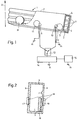
- Fig. 1 shows a device for checking the authenticity of coins, tokens or others metallic objects with a coin channel 1, preferably as a recess in a body 2 is formed from two plastic parts.
- the coin channel 1 is delimited by the bottom 3, one lower and an upper side wall 4 or 5 and a ceiling 6.
- the lower side wall 4 is with molded ribs 7 which are formed in the direction of the coin M.
- the coin channel 1 is inclined in the running direction of a coin M to be checked and the two side walls 4 and 5 are inclined to the vertical V by an acute angle of typically 12 °, so that the Checking coin M rolls down or down on the floor 3 along the coin channel 1 and thereby ideally lies flat with a side surface on the ribs 7 of the lower side wall 4.
- the Side walls 4 and 5 each have not shown on the side facing away from the coin channel 1 Recesses for receiving staggered coils 9 and 10 and, optionally, metallic Tiles 11, 12 on.
- the coil 9 and the plate 12 are located on the lower side wall 4, which is why they are drawn with dashed lines.
- the plates 11 and 12 are opposite the coils 9 and 10, respectively appropriate. They are preferably round or square, but can also be any other have geometric shape.
- One coil 9, 10 each and possibly the one in the opposite Sidewall 5 or 4 arranged metallic plates 11 and 12 form an inductive measuring element.
- the two coils 9 and 10 have two connections, one of which is connected to one common electrical ground connection m, the other is led to a switch 13 so that it connectable to an electronic circuit 14 for electrically independent operation are.
- the device also contains a control and evaluation unit 15, for example in the form of a Microprocessor for evaluating the output signal supplied by the electronic circuit 14 and to control the facility.
- the circuit 14 and the microprocessor 15 are in this regard configured to derive discrete values from the signals measured with the coils 9 and 10, which values from depend on the alloy or the thickness d of the coin M.
- the coin M is only considered genuine then and accepted by the test facility if these values are within specified tolerances predetermined values match, otherwise it is rejected.
- the microprocessor 15 controls the switch 13 so that when the coin M passes through the coils 9 and 10 signals occurring successively in time with a single electronic circuit 14 can be measured.
- the switch 13 and the common for both coils 9 and 10 Circuit 14 can, however, also have its own circuit 14 for each of coils 9 and 10, so that the working conditions for both coils 9 and 10 are separate and optimally selectable.
- the coil 9 is located on the lower side wall 4, on which the coin M moves along so that the distance between the coil 9 and the side surface of the coin M is fixed and is, for example, 1.1 mm.
- the coin M is made of either a single alloy or several alloys.
- the internal resistance R 9 of the coil 9 measured in the presence of the coin M depends almost exclusively on the material of the coin M when the frequency f of the current flowing through the coil 9 is selected appropriately.
- the distance between the coil 10 and the coin M depends on its thickness d.
- the internal resistance R 10 thus depends not only on the material of the coin M, but also on its thickness d. If the alloy of the coin M is known, the thickness d of the coin M can be clearly determined.
- the diameter of the coils 9 and 10 is smaller than the diameter the smallest coin M to be measured and is the coil on the side wall 4 or 5 of the coin channel 1 arranged at an appropriate height, so that the smallest coin M to be tested Briefly completely covers the coil during the passage.
- the diameter of the coil is e.g. 11 mm.
- the resistance of the lead wires is comparatively low.
- a single double coil 16 as an inductive measuring element serve.
- the double coil 16 consists of two individual coils 17 arranged on both sides of the coin channel 1 and 18, which are wound in opposite directions and are electrically connected in series so that the magnetic field generated within the coin channel 1 essentially parallel to the side walls 4 and 5 is.
- the coils 9 and 10 (FIG. 1), with or without an opposing metallic plate 11 or 12, as well as the double coil 16 (FIG. 2) each represent an inductive measuring element.
- the inductive measuring element is operated by the electronic circuit 14 and represents an electrical impedance Z S for it.
- the reference symbol S is used for the corresponding coil 9, 10 or 16 of the inductive measuring element.
- the internal resistance R S contains a static component R S, DC and a dynamic component R S, AC (f), which depends on the frequency f of the current flowing through the coil S, the physical properties of the coin M, and the geometry of the coil S, depends on the metallic plates 11, 12 (FIG. 1) which may be present and, in the case of an inductive measuring element with individual coils (9; 10) in particular, on the distance between the individual coil (9; 10) and the coin M. As soon as the coin M comes into the measuring range of the coil S while rolling along the coin channel 1, its internal resistance R S increases.
- the first connection of the coil S is connected to the ground m
- the second connection of the coil S is connected to a first current source 19 via a first capacitive element in the form of a capacitor C 1 , which delivers an alternating current I 1 with an approximately constant amplitude and with the frequency f 1 .
- the current source 19 is formed from a first AC voltage source 20 and a first resistor R 1 , which has a high resistance compared to the magnitude of the impedance Z S of the coil S.
- a connection of the current source 19 is connected to the ground m.
- the second connection of the coil S is further connected via a second capacitor C 2 to a second current source 21, which supplies an alternating current I 2 with an approximately constant amplitude and with the frequency f 2 .
- the second current source 21 is formed from an AC voltage source 22 and a second resistor R 2 , which is also high-resistance in comparison with the magnitude of the impedance Z S of the coil S.
- a connection of the current source 21 is also connected to the ground m.
- the inductance L S of the coil S is typically 0.5-2 mH.
- the AC voltage source 20 generates a voltage with a frequency f 1 of approximately 1-10 kHz and the AC voltage source 22 generates a voltage with a frequency f 2 of approximately 50-200 kHz.
- the frequencies f 1 and f 2 are around 50-200 kHz and 1 MHz, respectively.
- the frequency f 2 is approximately one to two orders of magnitude larger than the frequency f 1 .
- the zero point ⁇ 1.0 ie the value of the phase shift ⁇ 1 in the absence of coins M or in the presence of a coin M of a predetermined coin type, can be set as desired via the value of the capacitor C 1 .
- the value C 1 is chosen, for example, so that the zero point ⁇ 1.0 is 45 °, since the arctangent function has the greatest slope at 45 °.
- the zero point ⁇ 1.0 can also have the value 0 ° or any other value.
- the current flowing through the impedance Z 1 current I 1 is, for example, transformed by means of an operational amplifier 23 whose two inputs are connected to the two terminals of the resistor R1 into a voltage U R1.
- the voltage U Z1 across the impedance Z 1 is tapped by means of a further operational amplifier 24.
- the voltages U R1 and U Z1 at the outputs of the operational amplifiers 23 and 24 are fed via a filter 25 and 26 to a phase meter 27 which emits a signal proportional to the phase shift ⁇ 1 as the output signal.
- the filters 25 and 26 are dimensioned such that voltage signals with the frequency f 1 are passed, while signals with the frequency f 2 are filtered out.
- the phase shift ⁇ 1 can also be measured in another way.
- the coil S and the capacitor C 2 form a second impedance Z 2 .
- the phase shift ⁇ 2 between the current I 2 and the voltage U Z2 lying above the impedance Z 2 can be measured in an analog manner, the illustration of the corresponding electronic elements such as amplifiers and phase meters being omitted for the sake of clarity in the drawing.
- the frequency f 1 is preferably in the range from 1 to 10 kHz, the frequency f 2 in the range from 50 to 200 kHz. However, the frequency f 2 can also assume values that extend into the MHz range.
- the phase shifts ⁇ 1 and ⁇ 2 induced by the coin can thus be measured for each coin M. If necessary, the amounts of the impedances Z 1 and Z 2 can be determined as further variables characterizing the coin M.
- the capacitive elements C 1 , C 2 serve to reduce the imaginary part of the impedances Z 1 and Z 2 to a value at which a change caused by the coin M can be measured with great accuracy.
- the amounts of the impedances Z 1 , Z 2 are therefore smaller than the amount of the impedance Z S of the coil S alone.
- a circuit 28 and the evaluation of the signal supplied by it are described in the European patent application EP 704 825.
- the output signal of the circuit 28 is proportional to the current I 3 and thus to the ohmic internal resistance R S, AC (f R ), which is at Passage of the coin M changes.
- the current I 3 thus also serves as a criterion for accepting or rejecting the coin M.
- a total of four characteristic values for the coin M can be measured, namely the phase shift ⁇ 1 , the magnitude of the impedance Z 1 , the ohmic internal resistance R S, AC (f R ) of the coil S and the resonance frequency f R , or derived values.
- the capacitive elements C 1 and C 2 are advantageously dimensioned such that the current I 1 has a low frequency f 1 of a few kHz and that the resonance frequency f R is greater than the frequency f 1 by one to two orders of magnitude.
- the double coil 16 (FIG. 2) is used as an inductive measuring element
- the single coil 17 arranged on the lower side wall 4 is advantageously wound out of low-resistance stranded wire compared to a normal wire, so that its internal resistance R S, AC is as low as possible.
- Both exemplary embodiments have in common that on the one hand the coil S with a capacitive one Element is connected in series, with which it forms an electrical impedance, which with a first current is fed from a current source, and that the phase shift between the first Current and voltage over impedance as a criterion for acceptance or rejection of the Coin serves.
- the coil S is additionally supplied with a second current from a second current or Voltage source acts to measure further parameters of the coin. The measurement of The phase shift and the other parameters are almost independent of each other.
Landscapes
- Physics & Mathematics (AREA)
- General Physics & Mathematics (AREA)
- Testing Of Coins (AREA)
- Investigating Or Analyzing Materials By The Use Of Magnetic Means (AREA)
- Geophysics And Detection Of Objects (AREA)
Claims (10)
- Dispositif pour tester l'authenticité de pièces de monnaie (M), jetons ou autres articles plats de métal, ayant un élément de mesure inductif avec une bobine (S; 9; 10; 11; 12; 16) pour caractériser la pièce de monnaie, où la bobine (S; 9; 10; 16) peut être alimentée d'un premier courant (I1) à une première fréquence (f1) d'une première source de courant de tension (19) et dans lequel un élément capacitif (C1) est connecté entre la bobine (S; 9; 10; 16) et la première source de courant de tension (19), la bobine et l'élément capacitif (C1) formant une impédance Z1 et que le déphasage (ϕ1) entre le premier courant I1 et la tension à travers l'impédance Z1 sert de critère pour l'acceptation ou le rejet de la pièce de monnaie, caractérisé en ce que, pour la mesure d'autres paramètres (ϕ2, fR, Rs,AC (fR)) la bobine (S; 9; 10; 16) est alimentée d'un deuxième courant (I2, I3) d'une deuxième source de courant de tension (21, 28) à haute fréquence (f2).
- Dispositif selon la revendication 1, caractérisé en ce que l'élément capacitif (C1) est déterminé de telle sorte que le déphasage ϕ a une valeur prédéterminée selon l'absence ou la présence d'une pièce de monnaie d'un type de pièce de monnaie prédéterminé.
- Dispositif selon la revendication 1 ou 2, caractérisé en ce que un élément additionnel capacitif (C2) est connecté entre la bobine (S; 9; 10; 16) et la deuxième source de courant ou de tension (21), la bobine et l'élément additionnel capacitif (C2) formant une deuxième impédance Y (Z2) et que le déphasage ϕ entre le deuxième courant K (I2) et la tension à travers la deuxième impédance Y (Z2) sert d'un critère pour l'acceptation ou le rejet de la pièce de monnaie.
- Dispositif selon la revendication 1 ou 2, caractérisé en ce que un élément additionnel capacitif (C2) est connecté entre la bobine (S; 9; 10; 16) et la deuxième source de courant ou de tension (28), la bobine (S; 9; 10; 16) et l'élément additionnel capacitif (C2) formant un circuit de résonance série et en ce que la deuxième source de courant ou de tension (28) fait fonctionner le circuit de résonance série en résonance.
- Dispositif selon l'une des revendications 1 à 4, caractérisé en ce que la valeur de l'impédance Z (Z1) sert aussi de critère pour l'acceptation ou le rejet de la pièce de monnaie.
- Dispositif selon l'une des revendications 1 à 5, caractérisé en ce que la fréquence du premier courant J (I1) est dans la gamme de 1 à 10 kHz.
- Dispositif selon l'une des revendications 1 à 6, caractérisé en ce que la fréquence du deuxième courant K (I2; I3) est dans la gamme de 50 kHz à 5 MHz.
- Dispositif selon l'une des revendications 1 à 7, caractérisé en ce que l'élément de mesure inductif est formé par la bobine (S; 9; 10) qui est arrangé sur une paroi latérale (4; 5) d'un passage de pièce de monnaie (1) et par un plat de métal (11; 12) arrangé sur la paroi opposée (5; 4) du passage de pièce de monnaie (1).
- Dispositif selon l'une des revendications 1 à 7, caractérisé en ce que la bobine de l'élément de mesure inductif est une bobine double (16), comprenant deux bobines individuelles (17; 18) qui sont arrangées sur une partie basse et haute des parois latérales (4; 5) d'un passage de pièce de monnaie (1) et qui sont bobinées dans des directions opposées et connectées électriquement en série.
- Dispositif selon la revendication 9, caractérisé en ce que la bobine individuelle (17) disposée sur la paroi latérale inférieure (4) est bobinée avec du fil de faible résistance.
Applications Claiming Priority (3)
| Application Number | Priority Date | Filing Date | Title |
|---|---|---|---|
| CH86996 | 1996-04-03 | ||
| CH869/96 | 1996-04-03 | ||
| CH86996 | 1996-04-03 |
Publications (3)
| Publication Number | Publication Date |
|---|---|
| EP0805423A2 EP0805423A2 (fr) | 1997-11-05 |
| EP0805423A3 EP0805423A3 (fr) | 1997-11-12 |
| EP0805423B1 true EP0805423B1 (fr) | 2004-08-04 |
Family
ID=4197077
Family Applications (1)
| Application Number | Title | Priority Date | Filing Date |
|---|---|---|---|
| EP96107303A Expired - Lifetime EP0805423B1 (fr) | 1996-04-03 | 1996-05-09 | Dispositif pour déterminer la validité de pièces de monnaie, jetons ou autres objets plats métalliques |
Country Status (12)
| Country | Link |
|---|---|
| US (1) | US6145646A (fr) |
| EP (1) | EP0805423B1 (fr) |
| JP (1) | JP2000508793A (fr) |
| KR (1) | KR20000004949A (fr) |
| CN (1) | CN1107294C (fr) |
| AT (1) | ATE272875T1 (fr) |
| AU (1) | AU2693597A (fr) |
| CA (1) | CA2250412A1 (fr) |
| DE (1) | DE59611050D1 (fr) |
| RU (1) | RU2186422C2 (fr) |
| TW (1) | TW338821B (fr) |
| WO (1) | WO1997038400A1 (fr) |
Families Citing this family (4)
| Publication number | Priority date | Publication date | Assignee | Title |
|---|---|---|---|---|
| US6267662B1 (en) * | 1999-04-13 | 2001-07-31 | Mars Incorporated | Measuring a stack of coins in a coin handling device |
| ES2170678B1 (es) | 2000-06-30 | 2003-09-16 | Azkoyen Medios De Pago Sa | Metodo y aparato de obtencion de caracteristicas fisicas de monedas para su identificacion. |
| CN100414567C (zh) * | 2006-02-07 | 2008-08-27 | 上海造币厂 | 硬币类物体无损伤整体定值测量方法及专用测量仪 |
| EP2599059B1 (fr) * | 2010-07-27 | 2018-03-07 | Coin Acceptors, Inc. | Dispositif de détection |
Family Cites Families (12)
| Publication number | Priority date | Publication date | Assignee | Title |
|---|---|---|---|---|
| GB1483192A (en) * | 1973-11-22 | 1977-08-17 | Mars Inc | Arrival sensor |
| FR2305809A1 (fr) * | 1975-03-25 | 1976-10-22 | Crouzet Sa | Dispositif d'authentification de titres monetaires |
| KR820001292B1 (ko) * | 1978-11-14 | 1982-07-19 | 시시도 후꾸시게 | 경화 선별장치 |
| GR69124B (fr) * | 1980-02-06 | 1982-05-03 | Mars Inc | |
| US4469213A (en) * | 1982-06-14 | 1984-09-04 | Raymond Nicholson | Coin detector system |
| JPS60262292A (ja) * | 1984-06-08 | 1985-12-25 | 株式会社田村電機製作所 | 硬貨検査装置 |
| EP0505609B2 (fr) * | 1991-03-27 | 2004-03-17 | Nippon Conlux Co., Ltd. | Procédé et dispositif pour la sélection de pièces de monnaie |
| JP2948035B2 (ja) * | 1992-11-11 | 1999-09-13 | 株式会社日本コンラックス | コインの判別方法および判別装置 |
| US5433310A (en) * | 1994-01-04 | 1995-07-18 | Coin Mechanisms, Inc. | Coin discriminator with offset null coils |
| GB2287341B (en) * | 1994-03-11 | 1997-09-17 | Mars Inc | Money validation |
| KR0125052Y1 (ko) * | 1994-03-17 | 1998-12-01 | 안준철 | 주화선별장치 |
| ATE160639T1 (de) * | 1994-09-21 | 1997-12-15 | Landis & Gyr Tech Innovat | Einrichtung zur prüfung der echtheit von münzen, jetons oder anderen flachen metallischen gegenständen |
-
1996
- 1996-05-09 AT AT96107303T patent/ATE272875T1/de not_active IP Right Cessation
- 1996-05-09 DE DE59611050T patent/DE59611050D1/de not_active Expired - Fee Related
- 1996-05-09 EP EP96107303A patent/EP0805423B1/fr not_active Expired - Lifetime
-
1997
- 1997-04-02 CA CA002250412A patent/CA2250412A1/fr not_active Abandoned
- 1997-04-02 US US09/155,444 patent/US6145646A/en not_active Expired - Fee Related
- 1997-04-02 AU AU26935/97A patent/AU2693597A/en not_active Abandoned
- 1997-04-02 JP JP9535820A patent/JP2000508793A/ja active Pending
- 1997-04-02 WO PCT/EP1997/001663 patent/WO1997038400A1/fr not_active Ceased
- 1997-04-02 CN CN97193567A patent/CN1107294C/zh not_active Expired - Fee Related
- 1997-04-02 RU RU98120496/09A patent/RU2186422C2/ru not_active IP Right Cessation
- 1997-04-02 KR KR1019980707540A patent/KR20000004949A/ko not_active Ceased
- 1997-07-16 TW TW086110100A patent/TW338821B/zh active
Also Published As
| Publication number | Publication date |
|---|---|
| JP2000508793A (ja) | 2000-07-11 |
| WO1997038400A1 (fr) | 1997-10-16 |
| RU2186422C2 (ru) | 2002-07-27 |
| CN1217801A (zh) | 1999-05-26 |
| CA2250412A1 (fr) | 1997-10-16 |
| EP0805423A2 (fr) | 1997-11-05 |
| EP0805423A3 (fr) | 1997-11-12 |
| AU2693597A (en) | 1997-10-29 |
| KR20000004949A (ko) | 2000-01-25 |
| DE59611050D1 (de) | 2004-09-09 |
| ATE272875T1 (de) | 2004-08-15 |
| US6145646A (en) | 2000-11-14 |
| CN1107294C (zh) | 2003-04-30 |
| TW338821B (en) | 1998-08-21 |
Similar Documents
| Publication | Publication Date | Title |
|---|---|---|
| DE2612613C3 (de) | Verfahren und Schaltungsanordnung zum Identifizieren von Gegenständen, insbesondere von Münzen oder Wertpapieren | |
| DE3235114C2 (fr) | ||
| DE3600022C2 (de) | Münzunterscheidungsvorrichtung | |
| DE69010988T2 (de) | Münzprüfvorrichtung mit Kompensation der äusseren Umgebungsbedingungen. | |
| DE69034216T2 (de) | Verfahren und Vorrichtung zur Echtheitsprüfung von Geld | |
| DE2935539A1 (de) | Fuehleinrichtung fuer metallgegenstaende | |
| DE2654472A1 (de) | Muenzpruefgeraet | |
| EP3293499B1 (fr) | Procédé de fonctionnement d'un débitmètre magnétique inductif et débitmètre magnétique inductif | |
| DE69510140T2 (de) | Münzprüfung | |
| DE60222013T2 (de) | Münzunterscheidungsvorrichtung, in der frequenzen von wirbelströmen gemessen werden | |
| DE3815009C2 (fr) | ||
| EP0447653B1 (fr) | Capteur inductif de position | |
| CH676162A5 (fr) | ||
| EP0704825B1 (fr) | Dispositif pour déterminer l'authenticité de pièces de monnaie, de jetons ou d'autres objets métalliques plats | |
| DE102011015589B3 (de) | Anordnung und Verfahren zur kapazitiven Abtastung der Drehbwegung eines Drehelements | |
| DE10100624B4 (de) | System zur Fluidstandsmessung | |
| EP0805423B1 (fr) | Dispositif pour déterminer la validité de pièces de monnaie, jetons ou autres objets plats métalliques | |
| DE3231116A1 (de) | Verfahren und vorrichtung zur pruefung von muenzen mit der phasenverschiebung niedriger frequenzen | |
| DE2716740A1 (de) | Vorrichtung zur automatischen, beruehrungsfreien pruefung von muenzen auf echtheit und/oder nennwert und/oder zur rechnergefuehrten parameterauswertung | |
| DE69921349T2 (de) | Verbesserte münzannahmevorrichtung | |
| EP1108989B1 (fr) | Dispositif pour la mesure d'un débit d'un fluide de mesure dans un conduit de mesure | |
| DE102017128472A1 (de) | Induktiver Näherungsschalter und Verfahren zum Betreiben eines induktiven Näherungsschalters | |
| DE2916123A1 (de) | Schaltungsanordnung zur pruefung der groesse von materialzusammensetzung von muenzen | |
| DE4339543C2 (de) | Verfahren zur Prüfung von Münzen | |
| EP0888595B1 (fr) | Systeme pour verifier des pieces de monnaie |
Legal Events
| Date | Code | Title | Description |
|---|---|---|---|
| PUAI | Public reference made under article 153(3) epc to a published international application that has entered the european phase |
Free format text: ORIGINAL CODE: 0009012 |
|
| PUAL | Search report despatched |
Free format text: ORIGINAL CODE: 0009013 |
|
| AK | Designated contracting states |
Kind code of ref document: A2 Designated state(s): AT BE CH DE DK ES FI FR GB GR IE IT LI LU MC NL PT SE |
|
| AK | Designated contracting states |
Kind code of ref document: A3 Designated state(s): AT BE CH DE DK ES FI FR GB GR IE IT LI LU MC NL PT SE |
|
| 17P | Request for examination filed |
Effective date: 19980512 |
|
| RAP1 | Party data changed (applicant data changed or rights of an application transferred) |
Owner name: IP-TPG HOLDCO S.A.R.L. |
|
| 19U | Interruption of proceedings before grant |
Effective date: 20010206 |
|
| 19W | Proceedings resumed before grant after interruption of proceedings |
Effective date: 20020904 |
|
| RAP1 | Party data changed (applicant data changed or rights of an application transferred) |
Owner name: IPM INTERNATIONAL SA |
|
| 17Q | First examination report despatched |
Effective date: 20030721 |
|
| GRAP | Despatch of communication of intention to grant a patent |
Free format text: ORIGINAL CODE: EPIDOSNIGR1 |
|
| RTI1 | Title (correction) |
Free format text: DEVICE FOR CHECKING THE VALIDITY OF COINS, TOKENS OR OTHER FLAT METALLIC OBJECTS |
|
| RTI1 | Title (correction) |
Free format text: DEVICE FOR CHECKING THE VALIDITY OF COINS, TOKENS OR OTHER FLAT METALLIC OBJECTS |
|
| GRAS | Grant fee paid |
Free format text: ORIGINAL CODE: EPIDOSNIGR3 |
|
| GRAA | (expected) grant |
Free format text: ORIGINAL CODE: 0009210 |
|
| AK | Designated contracting states |
Kind code of ref document: B1 Designated state(s): AT BE CH DE DK ES FI FR GB GR IE IT LI LU MC NL PT SE |
|
| PG25 | Lapsed in a contracting state [announced via postgrant information from national office to epo] |
Ref country code: NL Free format text: LAPSE BECAUSE OF FAILURE TO SUBMIT A TRANSLATION OF THE DESCRIPTION OR TO PAY THE FEE WITHIN THE PRESCRIBED TIME-LIMIT Effective date: 20040804 Ref country code: IT Free format text: LAPSE BECAUSE OF FAILURE TO SUBMIT A TRANSLATION OF THE DESCRIPTION OR TO PAY THE FEE WITHIN THE PRE;WARNING: LAPSES OF ITALIAN PATENTS WITH EFFECTIVE DATE BEFORE 2007 MAY HAVE OCCURRED AT ANY TIME BEFORE 2007. THE CORRECT EFFECTIVE DATE MAY BE DIFFERENT FROM THE ONE RECORDED.SCRIBED TIME-LIMIT Effective date: 20040804 Ref country code: IE Free format text: LAPSE BECAUSE OF FAILURE TO SUBMIT A TRANSLATION OF THE DESCRIPTION OR TO PAY THE FEE WITHIN THE PRESCRIBED TIME-LIMIT Effective date: 20040804 Ref country code: GB Free format text: LAPSE BECAUSE OF FAILURE TO SUBMIT A TRANSLATION OF THE DESCRIPTION OR TO PAY THE FEE WITHIN THE PRESCRIBED TIME-LIMIT Effective date: 20040804 Ref country code: FR Free format text: LAPSE BECAUSE OF FAILURE TO SUBMIT A TRANSLATION OF THE DESCRIPTION OR TO PAY THE FEE WITHIN THE PRESCRIBED TIME-LIMIT Effective date: 20040804 Ref country code: FI Free format text: LAPSE BECAUSE OF FAILURE TO SUBMIT A TRANSLATION OF THE DESCRIPTION OR TO PAY THE FEE WITHIN THE PRESCRIBED TIME-LIMIT Effective date: 20040804 |
|
| REG | Reference to a national code |
Ref country code: GB Ref legal event code: FG4D Free format text: NOT ENGLISH |
|
| RIC1 | Information provided on ipc code assigned before grant |
Ipc: 7G 07D 5/08 A |
|
| REG | Reference to a national code |
Ref country code: CH Ref legal event code: EP |
|
| REG | Reference to a national code |
Ref country code: IE Ref legal event code: FG4D Free format text: GERMAN |
|
| REF | Corresponds to: |
Ref document number: 59611050 Country of ref document: DE Date of ref document: 20040909 Kind code of ref document: P |
|
| PG25 | Lapsed in a contracting state [announced via postgrant information from national office to epo] |
Ref country code: SE Free format text: LAPSE BECAUSE OF FAILURE TO SUBMIT A TRANSLATION OF THE DESCRIPTION OR TO PAY THE FEE WITHIN THE PRESCRIBED TIME-LIMIT Effective date: 20041104 Ref country code: GR Free format text: LAPSE BECAUSE OF FAILURE TO SUBMIT A TRANSLATION OF THE DESCRIPTION OR TO PAY THE FEE WITHIN THE PRESCRIBED TIME-LIMIT Effective date: 20041104 Ref country code: DK Free format text: LAPSE BECAUSE OF FAILURE TO SUBMIT A TRANSLATION OF THE DESCRIPTION OR TO PAY THE FEE WITHIN THE PRESCRIBED TIME-LIMIT Effective date: 20041104 |
|
| PG25 | Lapsed in a contracting state [announced via postgrant information from national office to epo] |
Ref country code: ES Free format text: LAPSE BECAUSE OF FAILURE TO SUBMIT A TRANSLATION OF THE DESCRIPTION OR TO PAY THE FEE WITHIN THE PRESCRIBED TIME-LIMIT Effective date: 20041115 |
|
| NLV1 | Nl: lapsed or annulled due to failure to fulfill the requirements of art. 29p and 29m of the patents act | ||
| GBV | Gb: ep patent (uk) treated as always having been void in accordance with gb section 77(7)/1977 [no translation filed] |
Effective date: 20040804 |
|
| REG | Reference to a national code |
Ref country code: IE Ref legal event code: FD4D |
|
| PG25 | Lapsed in a contracting state [announced via postgrant information from national office to epo] |
Ref country code: LU Free format text: LAPSE BECAUSE OF NON-PAYMENT OF DUE FEES Effective date: 20050509 Ref country code: AT Free format text: LAPSE BECAUSE OF NON-PAYMENT OF DUE FEES Effective date: 20050509 |
|
| PG25 | Lapsed in a contracting state [announced via postgrant information from national office to epo] |
Ref country code: MC Free format text: LAPSE BECAUSE OF NON-PAYMENT OF DUE FEES Effective date: 20050531 Ref country code: LI Free format text: LAPSE BECAUSE OF NON-PAYMENT OF DUE FEES Effective date: 20050531 Ref country code: CH Free format text: LAPSE BECAUSE OF NON-PAYMENT OF DUE FEES Effective date: 20050531 Ref country code: BE Free format text: LAPSE BECAUSE OF NON-PAYMENT OF DUE FEES Effective date: 20050531 |
|
| PLBE | No opposition filed within time limit |
Free format text: ORIGINAL CODE: 0009261 |
|
| STAA | Information on the status of an ep patent application or granted ep patent |
Free format text: STATUS: NO OPPOSITION FILED WITHIN TIME LIMIT |
|
| 26N | No opposition filed |
Effective date: 20050506 |
|
| EN | Fr: translation not filed | ||
| BERE | Be: lapsed |
Owner name: S.A. *IPM INTERNATIONAL Effective date: 20050531 |
|
| PG25 | Lapsed in a contracting state [announced via postgrant information from national office to epo] |
Ref country code: DE Free format text: LAPSE BECAUSE OF NON-PAYMENT OF DUE FEES Effective date: 20051201 |
|
| REG | Reference to a national code |
Ref country code: CH Ref legal event code: PL |
|
| BERE | Be: lapsed |
Owner name: S.A. *IPM INTERNATIONAL Effective date: 20050531 |
|
| PG25 | Lapsed in a contracting state [announced via postgrant information from national office to epo] |
Ref country code: PT Free format text: LAPSE BECAUSE OF NON-PAYMENT OF DUE FEES Effective date: 20050104 |