EP0806687A1 - Dispositif optomécanique et application à des capteurs en optique intégrée - Google Patents
Dispositif optomécanique et application à des capteurs en optique intégrée Download PDFInfo
- Publication number
- EP0806687A1 EP0806687A1 EP97401032A EP97401032A EP0806687A1 EP 0806687 A1 EP0806687 A1 EP 0806687A1 EP 97401032 A EP97401032 A EP 97401032A EP 97401032 A EP97401032 A EP 97401032A EP 0806687 A1 EP0806687 A1 EP 0806687A1
- Authority
- EP
- European Patent Office
- Prior art keywords
- optical
- mobile
- coupler
- distribution
- arms
- Prior art date
- Legal status (The legal status is an assumption and is not a legal conclusion. Google has not performed a legal analysis and makes no representation as to the accuracy of the status listed.)
- Withdrawn
Links
- 230000003287 optical effect Effects 0.000 title claims abstract description 35
- 239000013307 optical fiber Substances 0.000 claims description 30
- 238000009826 distribution Methods 0.000 claims description 25
- 238000012545 processing Methods 0.000 claims description 7
- 238000001514 detection method Methods 0.000 claims description 2
- 239000000835 fiber Substances 0.000 abstract description 19
- 239000000758 substrate Substances 0.000 abstract description 11
- 229910021421 monocrystalline silicon Inorganic materials 0.000 abstract description 2
- 230000001133 acceleration Effects 0.000 description 24
- 238000006073 displacement reaction Methods 0.000 description 24
- VYPSYNLAJGMNEJ-UHFFFAOYSA-N Silicium dioxide Chemical compound O=[Si]=O VYPSYNLAJGMNEJ-UHFFFAOYSA-N 0.000 description 14
- 238000000034 method Methods 0.000 description 13
- 238000004364 calculation method Methods 0.000 description 11
- 230000035945 sensitivity Effects 0.000 description 11
- 238000005530 etching Methods 0.000 description 9
- 238000005259 measurement Methods 0.000 description 7
- 238000000151 deposition Methods 0.000 description 6
- 238000004519 manufacturing process Methods 0.000 description 6
- 239000000377 silicon dioxide Substances 0.000 description 6
- 238000004518 low pressure chemical vapour deposition Methods 0.000 description 5
- OAICVXFJPJFONN-UHFFFAOYSA-N Phosphorus Chemical compound [P] OAICVXFJPJFONN-UHFFFAOYSA-N 0.000 description 4
- 230000000052 comparative effect Effects 0.000 description 4
- 230000008021 deposition Effects 0.000 description 4
- 239000000463 material Substances 0.000 description 4
- 229910052698 phosphorus Inorganic materials 0.000 description 4
- 230000005855 radiation Effects 0.000 description 4
- XUIMIQQOPSSXEZ-UHFFFAOYSA-N Silicon Chemical compound [Si] XUIMIQQOPSSXEZ-UHFFFAOYSA-N 0.000 description 3
- 230000008901 benefit Effects 0.000 description 3
- 238000006243 chemical reaction Methods 0.000 description 3
- 230000003071 parasitic effect Effects 0.000 description 3
- 239000011574 phosphorus Substances 0.000 description 3
- 230000004044 response Effects 0.000 description 3
- 238000004458 analytical method Methods 0.000 description 2
- 235000021183 entrée Nutrition 0.000 description 2
- 230000010354 integration Effects 0.000 description 2
- 238000007254 oxidation reaction Methods 0.000 description 2
- 238000001020 plasma etching Methods 0.000 description 2
- 229910052710 silicon Inorganic materials 0.000 description 2
- 239000010703 silicon Substances 0.000 description 2
- 229910052814 silicon oxide Inorganic materials 0.000 description 2
- JBRZTFJDHDCESZ-UHFFFAOYSA-N AsGa Chemical compound [As]#[Ga] JBRZTFJDHDCESZ-UHFFFAOYSA-N 0.000 description 1
- 229910017214 AsGa Inorganic materials 0.000 description 1
- XPDWGBQVDMORPB-UHFFFAOYSA-N Fluoroform Chemical compound FC(F)F XPDWGBQVDMORPB-UHFFFAOYSA-N 0.000 description 1
- 241001415961 Gaviidae Species 0.000 description 1
- 240000008042 Zea mays Species 0.000 description 1
- 239000000853 adhesive Substances 0.000 description 1
- 230000001070 adhesive effect Effects 0.000 description 1
- 230000004075 alteration Effects 0.000 description 1
- 238000013459 approach Methods 0.000 description 1
- QVGXLLKOCUKJST-UHFFFAOYSA-N atomic oxygen Chemical compound [O] QVGXLLKOCUKJST-UHFFFAOYSA-N 0.000 description 1
- 230000015572 biosynthetic process Effects 0.000 description 1
- 238000003776 cleavage reaction Methods 0.000 description 1
- 230000006835 compression Effects 0.000 description 1
- 238000007906 compression Methods 0.000 description 1
- 230000008878 coupling Effects 0.000 description 1
- 238000010168 coupling process Methods 0.000 description 1
- 238000005859 coupling reaction Methods 0.000 description 1
- 230000001419 dependent effect Effects 0.000 description 1
- 238000013461 design Methods 0.000 description 1
- 238000010586 diagram Methods 0.000 description 1
- 230000000694 effects Effects 0.000 description 1
- 230000014509 gene expression Effects 0.000 description 1
- 239000011521 glass Substances 0.000 description 1
- 239000003292 glue Substances 0.000 description 1
- 230000005484 gravity Effects 0.000 description 1
- BHEPBYXIRTUNPN-UHFFFAOYSA-N hydridophosphorus(.) (triplet) Chemical compound [PH] BHEPBYXIRTUNPN-UHFFFAOYSA-N 0.000 description 1
- 238000003384 imaging method Methods 0.000 description 1
- 238000005342 ion exchange Methods 0.000 description 1
- GQYHUHYESMUTHG-UHFFFAOYSA-N lithium niobate Chemical compound [Li+].[O-][Nb](=O)=O GQYHUHYESMUTHG-UHFFFAOYSA-N 0.000 description 1
- 230000000873 masking effect Effects 0.000 description 1
- 230000003647 oxidation Effects 0.000 description 1
- 229910052760 oxygen Inorganic materials 0.000 description 1
- 239000001301 oxygen Substances 0.000 description 1
- 238000000206 photolithography Methods 0.000 description 1
- 230000008569 process Effects 0.000 description 1
- 230000001902 propagating effect Effects 0.000 description 1
- 238000011160 research Methods 0.000 description 1
- 239000011347 resin Substances 0.000 description 1
- 229920005989 resin Polymers 0.000 description 1
- 230000007017 scission Effects 0.000 description 1
- LIVNPJMFVYWSIS-UHFFFAOYSA-N silicon monoxide Chemical compound [Si-]#[O+] LIVNPJMFVYWSIS-UHFFFAOYSA-N 0.000 description 1
- 238000004088 simulation Methods 0.000 description 1
- 230000003068 static effect Effects 0.000 description 1
- WFKWXMTUELFFGS-UHFFFAOYSA-N tungsten Chemical compound [W] WFKWXMTUELFFGS-UHFFFAOYSA-N 0.000 description 1
- 238000011144 upstream manufacturing Methods 0.000 description 1
Images




Classifications
-
- G—PHYSICS
- G02—OPTICS
- G02B—OPTICAL ELEMENTS, SYSTEMS OR APPARATUS
- G02B6/00—Light guides; Structural details of arrangements comprising light guides and other optical elements, e.g. couplings
- G02B6/24—Coupling light guides
- G02B6/26—Optical coupling means
- G02B6/30—Optical coupling means for use between fibre and thin-film device
-
- G—PHYSICS
- G01—MEASURING; TESTING
- G01H—MEASUREMENT OF MECHANICAL VIBRATIONS OR ULTRASONIC, SONIC OR INFRASONIC WAVES
- G01H9/00—Measuring mechanical vibrations or ultrasonic, sonic or infrasonic waves by using radiation-sensitive means, e.g. optical means
- G01H9/004—Measuring mechanical vibrations or ultrasonic, sonic or infrasonic waves by using radiation-sensitive means, e.g. optical means using fibre optic sensors
- G01H9/006—Measuring mechanical vibrations or ultrasonic, sonic or infrasonic waves by using radiation-sensitive means, e.g. optical means using fibre optic sensors the vibrations causing a variation in the relative position of the end of a fibre and another element
-
- G—PHYSICS
- G01—MEASURING; TESTING
- G01P—MEASURING LINEAR OR ANGULAR SPEED, ACCELERATION, DECELERATION, OR SHOCK; INDICATING PRESENCE, ABSENCE, OR DIRECTION, OF MOVEMENT
- G01P15/00—Measuring acceleration; Measuring deceleration; Measuring shock, i.e. sudden change of acceleration
- G01P15/02—Measuring acceleration; Measuring deceleration; Measuring shock, i.e. sudden change of acceleration by making use of inertia forces using solid seismic masses
- G01P15/08—Measuring acceleration; Measuring deceleration; Measuring shock, i.e. sudden change of acceleration by making use of inertia forces using solid seismic masses with conversion into electric or magnetic values
- G01P15/093—Measuring acceleration; Measuring deceleration; Measuring shock, i.e. sudden change of acceleration by making use of inertia forces using solid seismic masses with conversion into electric or magnetic values by photoelectric pick-up
-
- G—PHYSICS
- G02—OPTICS
- G02B—OPTICAL ELEMENTS, SYSTEMS OR APPARATUS
- G02B6/00—Light guides; Structural details of arrangements comprising light guides and other optical elements, e.g. couplings
- G02B6/10—Light guides; Structural details of arrangements comprising light guides and other optical elements, e.g. couplings of the optical waveguide type
- G02B6/12—Light guides; Structural details of arrangements comprising light guides and other optical elements, e.g. couplings of the optical waveguide type of the integrated circuit kind
- G02B6/122—Basic optical elements, e.g. light-guiding paths
-
- G—PHYSICS
- G02—OPTICS
- G02B—OPTICAL ELEMENTS, SYSTEMS OR APPARATUS
- G02B6/00—Light guides; Structural details of arrangements comprising light guides and other optical elements, e.g. couplings
- G02B6/24—Coupling light guides
- G02B6/36—Mechanical coupling means
- G02B6/3628—Mechanical coupling means for mounting fibres to supporting carriers
- G02B6/3648—Supporting carriers of a microbench type, i.e. with micromachined additional mechanical structures
- G02B6/3652—Supporting carriers of a microbench type, i.e. with micromachined additional mechanical structures the additional structures being prepositioning mounting areas, allowing only movement in one dimension, e.g. grooves, trenches or vias in the microbench surface, i.e. self aligning supporting carriers
-
- G—PHYSICS
- G02—OPTICS
- G02B—OPTICAL ELEMENTS, SYSTEMS OR APPARATUS
- G02B6/00—Light guides; Structural details of arrangements comprising light guides and other optical elements, e.g. couplings
- G02B6/24—Coupling light guides
- G02B6/26—Optical coupling means
- G02B6/28—Optical coupling means having data bus means, i.e. plural waveguides interconnected and providing an inherently bidirectional system by mixing and splitting signals
- G02B6/2804—Optical coupling means having data bus means, i.e. plural waveguides interconnected and providing an inherently bidirectional system by mixing and splitting signals forming multipart couplers without wavelength selective elements, e.g. "T" couplers, star couplers
- G02B6/2808—Optical coupling means having data bus means, i.e. plural waveguides interconnected and providing an inherently bidirectional system by mixing and splitting signals forming multipart couplers without wavelength selective elements, e.g. "T" couplers, star couplers using a mixing element which evenly distributes an input signal over a number of outputs
- G02B6/2813—Optical coupling means having data bus means, i.e. plural waveguides interconnected and providing an inherently bidirectional system by mixing and splitting signals forming multipart couplers without wavelength selective elements, e.g. "T" couplers, star couplers using a mixing element which evenly distributes an input signal over a number of outputs based on multimode interference effect, i.e. self-imaging
-
- G—PHYSICS
- G02—OPTICS
- G02B—OPTICAL ELEMENTS, SYSTEMS OR APPARATUS
- G02B6/00—Light guides; Structural details of arrangements comprising light guides and other optical elements, e.g. couplings
- G02B6/24—Coupling light guides
- G02B6/26—Optical coupling means
- G02B6/35—Optical coupling means having switching means
- G02B6/3502—Optical coupling means having switching means involving direct waveguide displacement, e.g. cantilever type waveguide displacement involving waveguide bending, or displacing an interposed waveguide between stationary waveguides
-
- G—PHYSICS
- G02—OPTICS
- G02B—OPTICAL ELEMENTS, SYSTEMS OR APPARATUS
- G02B6/00—Light guides; Structural details of arrangements comprising light guides and other optical elements, e.g. couplings
- G02B6/24—Coupling light guides
- G02B6/36—Mechanical coupling means
- G02B6/3628—Mechanical coupling means for mounting fibres to supporting carriers
- G02B6/3632—Mechanical coupling means for mounting fibres to supporting carriers characterised by the cross-sectional shape of the mechanical coupling means
- G02B6/3644—Mechanical coupling means for mounting fibres to supporting carriers characterised by the cross-sectional shape of the mechanical coupling means the coupling means being through-holes or wall apertures
-
- G—PHYSICS
- G02—OPTICS
- G02B—OPTICAL ELEMENTS, SYSTEMS OR APPARATUS
- G02B6/00—Light guides; Structural details of arrangements comprising light guides and other optical elements, e.g. couplings
- G02B6/24—Coupling light guides
- G02B6/36—Mechanical coupling means
- G02B6/3628—Mechanical coupling means for mounting fibres to supporting carriers
- G02B6/3684—Mechanical coupling means for mounting fibres to supporting carriers characterised by the manufacturing process of surface profiling of the supporting carrier
- G02B6/3692—Mechanical coupling means for mounting fibres to supporting carriers characterised by the manufacturing process of surface profiling of the supporting carrier with surface micromachining involving etching, e.g. wet or dry etching steps
-
- G—PHYSICS
- G02—OPTICS
- G02B—OPTICAL ELEMENTS, SYSTEMS OR APPARATUS
- G02B6/00—Light guides; Structural details of arrangements comprising light guides and other optical elements, e.g. couplings
- G02B6/24—Coupling light guides
- G02B6/42—Coupling light guides with opto-electronic elements
- G02B6/4201—Packages, e.g. shape, construction, internal or external details
- G02B6/4202—Packages, e.g. shape, construction, internal or external details for coupling an active element with fibres without intermediate optical elements, e.g. fibres with plane ends, fibres with shaped ends, bundles
Definitions
- the invention relates to the field of optomechanics.
- the invention relates to devices associating optical guides integrated with a mechanical structure engraved in the same material. These devices are particularly interesting in the field of metrology.
- Optomechanics is the result of a recent approach in the broader field of microtechnologies, even if the fields of integrated optics and micromechanics, taken separately, are well developed.
- the mechanical displacement of the end of an optical guide is used opposite the end of one or more fixed optical guides. It is the physical phenomenon to be measured (acceleration, vibrations, etc.) which causes this displacement of the end of the guide.
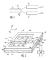
- a very simple configuration for measuring this displacement d consists in positioning, as illustrated in FIG. 1, an optical fiber 2, having one free end 4, opposite two optical fibers 6, 8 placed side by side. side.
- Each of these fibers transmits a signal S 1 , S 2 .
- a signal proportional to the acceleration undergone by the sensor is obtained by performing (electronically) the difference S 1 -S 2 of the two optical signals from the two output fibers.
- This device is simple, but poses certain problems.
- the device described above, in conjunction with FIG. 1, requires large displacements of the free end of the optical fiber. Indeed, the diameter of the optical fibers being of the order of 125 ⁇ m, the minimum distance between the two cores of the output optical fibers 6, 8 is 125 ⁇ m. The device is therefore only sensitive for fairly large displacements of the free end 4 of the optical fiber 2, and is therefore limited to low frequencies.
- This device has a sensitivity limited by the fairly large diameter of the fibers, which makes it impossible to bring the two output fibers together to obtain better sensitivity. Furthermore, this device is very delicate to produce because its performance is highly dependent on the correct positioning of the three fibers.
- the sensitivity is improved by the fact that it is possible to bring the two fixed output guides together. More precisely, the guides being produced by depositing and etching layers on a substrate, it is possible to produce two fixed output guides much closer to one another, moreover perfectly aligned with respect to the movable guide. This gives a more sensitive sensor or one that can measure higher frequencies.
- the invention provides an optomechanical device whose structure makes it possible to improve sensitivity compared to known devices.
- This device avoids the problems associated with coupling between neighboring outlet guides.
- the presence of a multimode coupler makes it possible, in a device according to the invention, to obtain better sensitivity to the same acceleration.
- the device according to the invention is therefore more sensitive to high vibration frequencies.
- the multimode coupler can be a multimode waveguide, or a set of monomode guides distributed so as to be able to exchange energy, suitable, when the distribution of the light beam which is directed at the input of the coupler comprises a single maximum , to transform this distribution into a distribution at N (N ⁇ 2) maximum at the output of the coupler.
- the N collection means arranged at the outlet of the coupler can be formed by optical guides or optical fibers or detectors, they can also be formed by a combination of two or three of these means.
- means may also be provided for delivering a signal representative of a combination of the signals Si, and for example a signal representative of the quantity ⁇ i S i , where ⁇ i is a weighting coefficient of the signal Si.
- the signal processing means can be provided to deliver a signal representative of the quantity S 1 -S 2 / S 1 + S 2 : an almost linear signal is then obtained over a greater range of displacements. of the movable guide.
- optical fibers may be provided, in the extension of these output optical guides.
- reflectors can be placed in front of the entrance to one of the fibers.
- the fibers can be inserted into holes made in the fixed part, these holes being widened in at least one place. These enlargements facilitate the supply of optical glue to hold the fibers.
- the light can be brought into the mobile part via an input optical fiber and an input optical guide.
- the device may also include reflectors at the output of the input optical fiber, on either side of the input optical guide.
- the mobile part In order to obtain greater displacements of the mobile part, it can be ballasted, in particular at its mobile end.
- means for compensating for the deformations of this part can be provided.
- These means may for example include at least one compensation arm, these arms having sufficient flexibility depending on the first direction (so as not to impede movement in this direction) and sufficient rigidity in the second direction (to limit deformation in this second direction).
- Various arm shapes can thus be envisaged ("U", square, straight shape).
- the invention also relates to an optomechanical sensor comprising a device as described above.
- the invention also applies to the production of an optical switch.
- electrical or electromagnetic control means are added to the mobile part, as described in document FR-2 660 444.
- the means of light collection include optical output guides, optical fibers and detectors.
- this device comprises a planar layer, or guide structure 10 (which may be composed of one or more layers), which is produced on a substrate 12, for example made of monocrystalline silicon, and which has a face of inlet E and an outlet face S parallel, obtained for example by cleavage.
- the guide structure 10 comprises for example a buffer layer 14 made of silicon oxide (8 to 12 ⁇ m thick), and an upper layer 16 made of silica (2 to 10 ⁇ m thick), the latter being able, for certain applications, to be replaced by air.
- the guide structure also comprises an input microguide 18 and two output microguides 20 and 22, made of silicon oxide doped for example with phosphorus, from 2 to 6 ⁇ m in height and from 2 to 8 ⁇ m in width as well as a multimode coupler 24 having substantially the same height (from 2 ⁇ m to 6 ⁇ m), for a width typically between 10 ⁇ m and 50 ⁇ m.
- the microguides 18, 20, 22 are parallel to a direction x itself parallel to the largest surface 9 of the planar layer or guide structure 10, and they are arranged on either side of a recess 26 passing through the structure guide 10.
- a guiding structure can be applied to other types of structures such as for example those obtained by ion exchange in substrates of the glass, lithium niobate type. or by deposition or etching of layers of the silica type, Si 3 N 4 , SiO x N y , AsGa, InP, etc.
- the recess 26 defines, in the guiding structure 10 and the substrate 12, a flexible beam 28 oriented at rest parallel to the direction x, this beam being able to move in the recess 26 in a direction y, parallel to the surface 9 of the guide structure and perpendicular to the direction x.
- This beam 28 comprises a fixed end 30, integral with the fixed part, and a free end 32 able to move in the recess 26.
- a central microguide 34 extends over the entire length of the beam 28, its end 36 opening out at the end 32 thereof.
- the multimode coupler 24 is disposed opposite the end 36 of the microguide 34.
- the term “multimode coupler” means a coupler or a multimode guide having several propagation modes or several single-mode guides.
- the multimode coupler 24 can be straight (FIG. 3) but it can also have the shape of a funnel, as illustrated in broken lines in FIG. 3.
- the multimode coupler 24 has an axis of symmetry, identified in Figure 3 by the axis (AA '), whether the guide is straight or funnel-shaped.
- the length L of the multimode coupler 24 is such that an optical signal, coming from the microguide of the mobile part (flexible beam) is transmitted to the N means of collecting light.
- L is such that, when an incident beam I directed on the input section of the coupler has an intensity distribution comprising a single maximum, an output beam having a number N of maximum is obtained, with N ⁇ 2.
- the multimode coupler can also determine the length necessary to obtain a distribution of intensity with several maxima at output for a distribution with only one maximum at input, by applying digital type methods such as the "beam propagation method "(BPM) and its variants, described in the article by MD Feit et al. ("Light propagation in graded-index optical fibers", Applied Optics 1978, vol.17, n ° 24, pp. 3990-3998), by GR Hadley ("Transparent boundary condition for beam propagation", Optics Letters, 1991, vol . 16, n ° 9, pp. 624-626) and in the article by Chung et al. ("An assessment of Finite Difference Beam propagation method", IEEE Journal of Quantum Electronics, vol.
- BPM beam propagation method
- the neighboring single-mode guides must be located at a distance of less than 10 ⁇ m from one another, preferably less than 5 ⁇ m.
- the width of a single single-mode guide is approximately 1 to 2 ⁇ m.
- FIGS. 5A to 5C relate to an example of a coupler for which the width W and the length L are chosen so that, if the system is at rest, that is to say if the input beam I E has a distribution intensity at a single maximum, centered on the axis of symmetry of the coupler, an intensity distribution is obtained with 4 maxima, at 4 points M 1 , M 2 , M 3 , M 4 , distributed symmetrically with respect to to the axis of symmetry of the coupler (we also say that we obtain 4 images at output).
- FIG. 5A schematically represents the distribution of the intensities at the input and at the output of the coupler
- FIG. 5B represents in a more detailed manner the distribution of the images at output.
- FIG. 5C represents the evolution of the detailed distribution of the intensity at the output of the coupler.
- An optical signal is produced by a radiation source (for example at the wavelength 0.78 ⁇ m) not shown in FIG. 2, then is transmitted by an input optical fiber 17 and by the microguide 18 then 34 in direction of the multimode coupler 24.
- Each output microguide is positioned at the location of a maximum, at the output of the coupler, when the beam input is in position centered on the input of the coupler.
- Each detector delivers a signal representative of the optical signal transmitted by the optical fiber at the output of which it is arranged. Finally, these detectors are connected to means 46 for processing the signals which they deliver.
- the processing of the signals by the means 46 can be carried out in several ways. One can, for example, digitize each signal delivered by a photodetector (and this using an analog-digital converter) and then carry out the processing in digital form using a microprocessor.
- the signals delivered by the photodetectors can also be processed analogically using circuits of the amplifier or operational amplifier type.
- the device 46 also includes means for carrying out various operations on the quantities measured, in particular operations for combining these quantities with one another (a combination is for example then formed, where ⁇ i is a weighting coefficient of the signal Si coming from the detector i). It can also obviously integrate any means necessary for memorizing the data.
- the free end of the beam 28 moves in the direction y, which modifies the distribution of the radiation at the output of the multimode coupler, therefore of the radiation transmitted by the N output guides. 20, 22, and therefore the signal produced by the detectors 42, 44.
- the displacement dy of a seismic mass as a function of the frequency has, generally, the shape of FIG. 6.
- the dimensioning of the seismic mass amounts to fixing the geometric dimensions of the structure to obtain a certain displacement d y , when it is subjected to an acceleration ⁇ .
- This comparative example shows that the introduction of a multimode coupler makes it possible to highlight displacements of the microbeam to which a conventional device is not sensitive.
- the use of a multimode guide makes it possible to avoid a loss of part of the light energy coming from the mobile guide: the signal / noise ratio is thereby improved.
- FIG. 9A which represents a device according to the invention, seen from above (the numerical references are the same as in FIG. 2), it is possible to add reflectors 60, 62, 64, 66, of on either side of each outlet guide 20, 22, and in front of the connection of these guides to the outlet optical fibers 38, 40.
- FIG. 9B represents the end of the single output guide 20, the connection to the optical fiber 38 and two reflectors 60, 62.
- the latter are, in the example illustrated in FIG. 9B, rectangles hollowed out in the device during the same production step as that of the mechanical structure (structures 14, 16 and guides 20, 22) and holes for receiving the fibers.
- the reflectors must have a refractive index n 2 lower than the refractive index n 1 of the surrounding medium.
- an optical fiber is characterized by its cone of acceptance of angle ⁇ . Yes the angle of a ray is less than the angle of this cone of acceptance ⁇ , then the ray enters the output optical fiber and is guided. If its angle is greater than ⁇ , then it is not guided by the output optical fiber.
- the reflectors will therefore make it possible to reflect the parasitic rays whose angles are in the cone of acceptance of the optical fiber when the angle ⁇ which its main side makes with the axis of the guide 20 and of the fiber 38 will be such that: where n 2 is the index of the reflector and n 1 the index of the guide layer or structure.
- n 2 is less than n 1, the more the reflector will reflect a large angular range. It is therefore advantageous to take n 2 as low as possible (therefore air or vacuum).
- the rays outside the cone thus defined are parasitic rays which do not enter the fiber.
- the corresponding locations are hollowed out at the same time as the fiber connection areas.
- connection area 37 provided for a fiber 38 can also be widened to certain locations 37a, 37b, 37c, 37d to facilitate the supply of optical adhesive allowing the fibers to be held in place.
- the widenings 37a-37d are made at the same time as the connection area 37. This can apply to each connection area of a fiber.
- the shape of the beams can also be modified so as to increase the sensitivity and / or to overcome the problems of parasitic deformation and sensitivity along the z axis (vertical or perpendicular to the plane 9 of the device).
- the beam can be ballasted.
- One way to ballast the beam is to have a larger free end 64. This results in a beam of greater mass and, therefore, for the same acceleration, greater displacements of the free end. This makes it easier to detect very weak accelerations.
- FIG. 11A Another problem is related to the sensitivity of the beam along the z axis, that is to say in a direction perpendicular to the plane of the device.
- the stage of production of the beam can lead to a stress gradient in the vertical direction z, which is the source of a deformation of the system. This is particularly the case when the beam is made of silica, obtained by PECVD deposition, with different phosphorous dopings.
- FIG. 11A where the numerical references identical to those of FIG. 2 designate the same elements there.
- This figure represents the structure obtained before the step of clearing the beam.
- ⁇ 2 denotes the stress at the 12-thin layer substrate interface (14, 34, 16) and ⁇ 1 denotes the stress at surface of the thin layer.
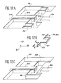
- FIG. 12A A first solution to these problems, falling within the scope of the present invention, is illustrated in FIG. 12A.
- Identical references to those of FIG. 2 represent the same elements there, but the assembly is represented in a more schematic manner.
- the compensation system consists of two arms 50, 52 which connect the free end of the beam 28 to the rest of the structure 10, which is a fixed part, since it is connected to the silicon substrate 12.
- each arm 50, 52 can consist of a body 51 in a "U" shape, a branch 53, 55 being added to the free end and in a manner substantially perpendicular to each branch side of the "U".
- the free end of one of these branches 53, 55 is connected to the beam 28, the free end of the other branch is connected to the rest of the guide structure 10. The same goes for the second compensating arm.
- the geometry of the compensating arms can be envisaged in various ways.
- the arms are rather chosen rigid in the vertical direction (direction z) and flexible in the horizontal direction (plane xy).
- We can play on the geometry of the arms by increasing the height / width form factor, the height h and the width 1 being identified in FIG. 12B as being respectively the height of the section of the compensating arm in a vertical section (along a plane parallel to zx), and the width of the compensating arm in the same vertical section.
- this form factor one can obtain sufficient flexibility, in the xy plane, so as not to impede the displacements of the beam in this same plane and sufficient rigidity, in the z direction, to limit the deformations of the beam. following this same direction.
- the arms are straight, or straight.
- FIG. 12C Another embodiment of the compensating arms is illustrated in FIG. 12C.
- each arm is approximately square-shaped with two segments substantially perpendicular to each other. Again, we will play on the aspect ratio height / width of the section of each arm, so as to give it the desired rigidity in the vertical direction, and the desired flexibility in the horizontal plane.
- the system can also operate with a single compensating arm.
- a preferred embodiment is that in which the system is symmetrical in the horizontal plane (as in FIGS. 12A and 12C, with respect to a median plane parallel to zOx). More generally, if the mobile part whose deformations are to be corrected has a certain spatial symmetry, it is desirable that the compensation system has the same symmetry. This geometry makes it possible to avoid small lateral deformations which could appear by buckling of the arms, because that the silica, or the material constituting the movable part, is generally in compression.
- the compensation arms are produced, for example, at the same time as the main beam, by etching. Only the geometry of the engraving mask changes.
- ballast elements such as the elements 70, 72 of FIG. 13
- the central beam and these elements 70, 72 are released. simultaneously with making the connection holes for the optical fibers.
- the etching depth, and therefore the etching time are determined by the diameter of the fiber. This time is generally less than the time necessary to clear the mechanical structure, if the latter also incorporates ballast elements.
- the beams are integral, that is to say that the part of the compensating arms, perpendicular to the axis of the beam, does not deform.
- the length of the perpendicular arms is, typically, on the order of five times shorter than the length of the parallel arms, and that the deformation is generally proportional to the cube of this length.
- the total deformation of the beam is the sum of the four deformations calculated separately. Finally, the torques imposed at the ends are determined by imposing zero deformation angles at the two ends of the total deformation.
- the fourth step is to find the constants A 0 , A 1 , B 0 , B 1 .
- FIG. 16 gives an example of deformation obtained for a compensated silica beam, not ballasted, under the effect of an acceleration of 400 m / s 2 .
- the beam is 2 mm long, 10 ⁇ m wide, and the compensating arms are 500 ⁇ m long.
- the different curves are obtained for widths "1" of different compensating arms. According to the maximum tolerated amplitude of the deformation, we will retain arms having the necessary width. It is also possible to calculate the deformation as a function of another parameter (for example, the length b of the compensation arms) in order to deduce the value of said parameter, to be chosen to obtain a certain maximum amplitude of the deformation.
- another parameter for example, the length b of the compensation arms
- the applications of the devices according to the invention are essentially in the field of optomechanical sensors.
- accelerometers or else vibration detectors the deviation of the moving part, or beam, makes it possible to detect an acceleration or a vibration.
- the invention can also be applied to microphones or else to the measurement of pressures, which implement the detection of vibrations or of a deformation applied to a moving part.
Landscapes
- Physics & Mathematics (AREA)
- General Physics & Mathematics (AREA)
- Optics & Photonics (AREA)
- Engineering & Computer Science (AREA)
- Microelectronics & Electronic Packaging (AREA)
- Chemical & Material Sciences (AREA)
- Crystallography & Structural Chemistry (AREA)
- Optical Couplings Of Light Guides (AREA)
- Mechanical Light Control Or Optical Switches (AREA)
- Optical Integrated Circuits (AREA)
Applications Claiming Priority (2)
| Application Number | Priority Date | Filing Date | Title |
|---|---|---|---|
| FR9605842 | 1996-05-10 | ||
| FR9605842A FR2748578B1 (fr) | 1996-05-10 | 1996-05-10 | Dispositif optomecanique et application a des capteurs en optique integree |
Publications (1)
| Publication Number | Publication Date |
|---|---|
| EP0806687A1 true EP0806687A1 (fr) | 1997-11-12 |
Family
ID=9492017
Family Applications (1)
| Application Number | Title | Priority Date | Filing Date |
|---|---|---|---|
| EP97401032A Withdrawn EP0806687A1 (fr) | 1996-05-10 | 1997-05-07 | Dispositif optomécanique et application à des capteurs en optique intégrée |
Country Status (4)
| Country | Link |
|---|---|
| US (1) | US5926591A (ja) |
| EP (1) | EP0806687A1 (ja) |
| JP (1) | JPH1054916A (ja) |
| FR (1) | FR2748578B1 (ja) |
Cited By (2)
| Publication number | Priority date | Publication date | Assignee | Title |
|---|---|---|---|---|
| EP1098213A1 (en) * | 1999-11-02 | 2001-05-09 | Corning Incorporated | Method of making pigtail arrays |
| EP1037024A3 (en) * | 1999-03-18 | 2007-06-20 | Meritor Heavy Vehicle Systems, LLC | Electromagnetic vibration sensor |
Families Citing this family (35)
| Publication number | Priority date | Publication date | Assignee | Title |
|---|---|---|---|---|
| US6807331B2 (en) * | 2000-09-19 | 2004-10-19 | Newport Opticom, Inc. | Structures that correct for thermal distortion in an optical device formed of thermally dissimilar materials |
| FR2819594B1 (fr) * | 2001-01-15 | 2003-05-16 | Opsitech Optical System Chip | Structure optique a poutre isolee et son procede de fabrication |
| US7492463B2 (en) | 2004-04-15 | 2009-02-17 | Davidson Instruments Inc. | Method and apparatus for continuous readout of Fabry-Perot fiber optic sensor |
| US7864329B2 (en) | 2004-12-21 | 2011-01-04 | Halliburton Energy Services, Inc. | Fiber optic sensor system having circulators, Bragg gratings and couplers |
| US7835598B2 (en) | 2004-12-21 | 2010-11-16 | Halliburton Energy Services, Inc. | Multi-channel array processor |
| US8519945B2 (en) | 2006-01-06 | 2013-08-27 | Pixtronix, Inc. | Circuits for controlling display apparatus |
| US9158106B2 (en) | 2005-02-23 | 2015-10-13 | Pixtronix, Inc. | Display methods and apparatus |
| US9229222B2 (en) * | 2005-02-23 | 2016-01-05 | Pixtronix, Inc. | Alignment methods in fluid-filled MEMS displays |
| US9082353B2 (en) | 2010-01-05 | 2015-07-14 | Pixtronix, Inc. | Circuits for controlling display apparatus |
| US8310442B2 (en) | 2005-02-23 | 2012-11-13 | Pixtronix, Inc. | Circuits for controlling display apparatus |
| US7999994B2 (en) | 2005-02-23 | 2011-08-16 | Pixtronix, Inc. | Display apparatus and methods for manufacture thereof |
| US9261694B2 (en) | 2005-02-23 | 2016-02-16 | Pixtronix, Inc. | Display apparatus and methods for manufacture thereof |
| US20070205969A1 (en) | 2005-02-23 | 2007-09-06 | Pixtronix, Incorporated | Direct-view MEMS display devices and methods for generating images thereon |
| EP1869737B1 (en) | 2005-03-16 | 2021-05-12 | Davidson Instruments, Inc. | High intensity fabry-perot sensor |
| WO2007033069A2 (en) | 2005-09-13 | 2007-03-22 | Davidson Instruments Inc. | Tracking algorithm for linear array signal processor for fabry-perot cross-correlation pattern and method of using same |
| US8526096B2 (en) | 2006-02-23 | 2013-09-03 | Pixtronix, Inc. | Mechanical light modulators with stressed beams |
| US7684051B2 (en) | 2006-04-18 | 2010-03-23 | Halliburton Energy Services, Inc. | Fiber optic seismic sensor based on MEMS cantilever |
| US7743661B2 (en) | 2006-04-26 | 2010-06-29 | Halliburton Energy Services, Inc. | Fiber optic MEMS seismic sensor with mass supported by hinged beams |
| US8115937B2 (en) | 2006-08-16 | 2012-02-14 | Davidson Instruments | Methods and apparatus for measuring multiple Fabry-Perot gaps |
| US9176318B2 (en) | 2007-05-18 | 2015-11-03 | Pixtronix, Inc. | Methods for manufacturing fluid-filled MEMS displays |
| US7787128B2 (en) | 2007-01-24 | 2010-08-31 | Halliburton Energy Services, Inc. | Transducer for measuring environmental parameters |
| US8169679B2 (en) | 2008-10-27 | 2012-05-01 | Pixtronix, Inc. | MEMS anchors |
| CN101482575B (zh) * | 2009-02-23 | 2011-02-09 | 东南大学 | 一种悬臂梁结构的谐振式集成光波导加速度计 |
| CN102378732B (zh) * | 2009-03-31 | 2016-02-03 | 西门子公司 | 带有梁形元件的可振动的微机械系统 |
| BR112012019383A2 (pt) | 2010-02-02 | 2017-09-12 | Pixtronix Inc | Circuitos para controlar aparelho de exibição |
| US8904867B2 (en) * | 2010-11-04 | 2014-12-09 | Qualcomm Mems Technologies, Inc. | Display-integrated optical accelerometer |
| US9134552B2 (en) | 2013-03-13 | 2015-09-15 | Pixtronix, Inc. | Display apparatus with narrow gap electrostatic actuators |
| US9778042B2 (en) | 2013-12-13 | 2017-10-03 | Intel Corporation | Opto-mechanical inertial sensor |
| US9341644B2 (en) * | 2013-12-13 | 2016-05-17 | Intel Corporation | MEMS apparatus with a movable waveguide section |
| US9285391B2 (en) | 2013-12-13 | 2016-03-15 | Intel Corporation | Optomechanical inertial sensor |
| US9239340B2 (en) | 2013-12-13 | 2016-01-19 | Intel Corporation | Optomechanical sensor for accelerometry and gyroscopy |
| WO2018005959A1 (en) | 2016-06-30 | 2018-01-04 | Acacia Communications, Inc. | Cantilevers with one-or two-dimensional actuation for on-chip active waveguide coupling alignment |
| CN109470885B (zh) * | 2018-10-19 | 2020-11-24 | 浙江大学 | 一种单片集成光学加速度计 |
| CN110207806B (zh) * | 2019-07-10 | 2021-10-26 | 国网上海市电力公司 | 一种斜角端面光纤振动传感器及其测量振动的方法 |
| US11965905B2 (en) * | 2021-12-22 | 2024-04-23 | Advanced Semiconductor Engineering, Inc. | Electronic module including optical motion sensor |
Citations (3)
| Publication number | Priority date | Publication date | Assignee | Title |
|---|---|---|---|---|
| JPS59151025A (ja) * | 1983-02-18 | 1984-08-29 | Shimadzu Corp | 振動センサ |
| DE4136510A1 (de) * | 1991-11-06 | 1993-05-13 | Battelle Institut E V | Beschleunigungssensor |
| DE4230087A1 (de) * | 1992-09-09 | 1994-03-10 | Bezzaoui Hocine Dipl Ing | Integrierte optisch/mikromechanische Sensoren |
Family Cites Families (2)
| Publication number | Priority date | Publication date | Assignee | Title |
|---|---|---|---|---|
| FR2660444B1 (fr) * | 1990-03-27 | 1992-10-16 | Commissariat Energie Atomique | Commutateur et systeme de commutation optiques multivoies integres et procede de fabrication du commutateur. |
| FR2729232A1 (fr) * | 1995-01-10 | 1996-07-12 | Commissariat Energie Atomique | Dispositif optique pour application optomecanique |
-
1996
- 1996-05-10 FR FR9605842A patent/FR2748578B1/fr not_active Expired - Fee Related
-
1997
- 1997-04-22 US US08/837,852 patent/US5926591A/en not_active Expired - Fee Related
- 1997-05-07 EP EP97401032A patent/EP0806687A1/fr not_active Withdrawn
- 1997-05-08 JP JP9133000A patent/JPH1054916A/ja not_active Withdrawn
Patent Citations (3)
| Publication number | Priority date | Publication date | Assignee | Title |
|---|---|---|---|---|
| JPS59151025A (ja) * | 1983-02-18 | 1984-08-29 | Shimadzu Corp | 振動センサ |
| DE4136510A1 (de) * | 1991-11-06 | 1993-05-13 | Battelle Institut E V | Beschleunigungssensor |
| DE4230087A1 (de) * | 1992-09-09 | 1994-03-10 | Bezzaoui Hocine Dipl Ing | Integrierte optisch/mikromechanische Sensoren |
Non-Patent Citations (2)
| Title |
|---|
| JENKINS R M ET AL: "A NOVEL WAVEGUIDE MACH-ZEHNDER INTERFEROMETER BASED ON MULTIMODE INTERFERENCE PHENOMENA", OPTICS COMMUNICATIONS, vol. 110, no. 3/04, 15 August 1994 (1994-08-15), pages 410 - 424, XP000454981 * |
| PATENT ABSTRACTS OF JAPAN vol. 008, no. 286 (P - 324) 27 December 1984 (1984-12-27) * |
Cited By (3)
| Publication number | Priority date | Publication date | Assignee | Title |
|---|---|---|---|---|
| EP1037024A3 (en) * | 1999-03-18 | 2007-06-20 | Meritor Heavy Vehicle Systems, LLC | Electromagnetic vibration sensor |
| EP1098213A1 (en) * | 1999-11-02 | 2001-05-09 | Corning Incorporated | Method of making pigtail arrays |
| WO2001033271A1 (en) * | 1999-11-02 | 2001-05-10 | Corning Incorporated | Method of making pigtail arrays |
Also Published As
| Publication number | Publication date |
|---|---|
| FR2748578B1 (fr) | 1998-05-29 |
| FR2748578A1 (fr) | 1997-11-14 |
| JPH1054916A (ja) | 1998-02-24 |
| US5926591A (en) | 1999-07-20 |
Similar Documents
| Publication | Publication Date | Title |
|---|---|---|
| EP0806687A1 (fr) | Dispositif optomécanique et application à des capteurs en optique intégrée | |
| EP0007312B1 (en) | Optical sensing apparatus | |
| US4342907A (en) | Optical sensing apparatus and method | |
| US6925213B2 (en) | Micromachined fiber optic sensors | |
| EP3147673B1 (fr) | Capteur physique opto-mecanique a sensibilite amelioree | |
| CN115524040B (zh) | 一种基于光纤的超灵敏应力传感器结构及系统 | |
| EP3769056B1 (en) | Diaphragm-based fiber acoustic sensor | |
| CN112888918B (zh) | 用于声学感测的聚合物涂布的高折射率波导 | |
| EP0647311B1 (fr) | Gyrometre optique a effet sagnac en structure completement integree | |
| CN112924143A (zh) | 一种光子芯片晶圆级测试装置和方法 | |
| EP0228315B1 (fr) | Dispositif interferométrique en anneau réciproque à fibre optique monomode | |
| CN118424446B (zh) | 腔光力振动传感器、测量装置及测量方法 | |
| EP3486603B1 (fr) | Système de transduction d'un déplacement en un déphasage optique | |
| Afshar et al. | Self-Aligning Optical MEMS Acoustic Sensors With nPa/√ Hz Resolution | |
| US6320992B1 (en) | Integrated optic accelerometer and method | |
| EP3968066A1 (fr) | Guide d'onde comportant une fibre optique multimode et adapte a concentrer spatialement les modes guides | |
| WO2022053712A1 (en) | Mach-zehnder interferometer sensor and measurement unit | |
| Michels et al. | Cavity optical transducer platform with integrated actuation for multiple sensing applications | |
| Sabac et al. | Design, testing, and calibration of an integrated Mach-Zehnder-based optical read-out architecture for MEMS characterization | |
| JPH0682325A (ja) | 光集積センサ | |
| RU2739829C1 (ru) | Оптомеханический вибрационный микродатчик | |
| Gorecki et al. | The role of fiber sensing technologies in MEMS/MOEMS | |
| Gorecki | Micromachining technology in optoelectronic sensing technologies | |
| EP4630762A1 (fr) | Dispositif de mesure d'une grandeur physique utilisant l'effet vernier optique | |
| Benaissa et al. | Simulation and fabrication of ARROW directional couplers |
Legal Events
| Date | Code | Title | Description |
|---|---|---|---|
| PUAI | Public reference made under article 153(3) epc to a published international application that has entered the european phase |
Free format text: ORIGINAL CODE: 0009012 |
|
| AK | Designated contracting states |
Kind code of ref document: A1 Designated state(s): DE ES GB IT |
|
| 17P | Request for examination filed |
Effective date: 19980417 |
|
| GRAP | Despatch of communication of intention to grant a patent |
Free format text: ORIGINAL CODE: EPIDOSNIGR1 |
|
| STAA | Information on the status of an ep patent application or granted ep patent |
Free format text: STATUS: THE APPLICATION IS DEEMED TO BE WITHDRAWN |
|
| 18D | Application deemed to be withdrawn |
Effective date: 20050826 |