EP0806799A1 - Procédé de formation d'interconnexions dans un circuit intégré - Google Patents
Procédé de formation d'interconnexions dans un circuit intégré Download PDFInfo
- Publication number
- EP0806799A1 EP0806799A1 EP97410048A EP97410048A EP0806799A1 EP 0806799 A1 EP0806799 A1 EP 0806799A1 EP 97410048 A EP97410048 A EP 97410048A EP 97410048 A EP97410048 A EP 97410048A EP 0806799 A1 EP0806799 A1 EP 0806799A1
- Authority
- EP
- European Patent Office
- Prior art keywords
- photo
- dielectric layer
- layer
- integrated circuit
- contact plugs
- Prior art date
- Legal status (The legal status is an assumption and is not a legal conclusion. Google has not performed a legal analysis and makes no representation as to the accuracy of the status listed.)
- Granted
Links
Images

Classifications
-
- H—ELECTRICITY
- H10—SEMICONDUCTOR DEVICES; ELECTRIC SOLID-STATE DEVICES NOT OTHERWISE PROVIDED FOR
- H10W—GENERIC PACKAGES, INTERCONNECTIONS, CONNECTORS OR OTHER CONSTRUCTIONAL DETAILS OF DEVICES COVERED BY CLASS H10
- H10W20/00—Interconnections in chips, wafers or substrates
- H10W20/01—Manufacture or treatment
-
- H—ELECTRICITY
- H10—SEMICONDUCTOR DEVICES; ELECTRIC SOLID-STATE DEVICES NOT OTHERWISE PROVIDED FOR
- H10P—GENERIC PROCESSES OR APPARATUS FOR THE MANUFACTURE OR TREATMENT OF DEVICES COVERED BY CLASS H10
- H10P50/00—Etching of wafers, substrates or parts of devices
- H10P50/20—Dry etching; Plasma etching; Reactive-ion etching
- H10P50/26—Dry etching; Plasma etching; Reactive-ion etching of conductive or resistive materials
- H10P50/264—Dry etching; Plasma etching; Reactive-ion etching of conductive or resistive materials by chemical means
- H10P50/266—Dry etching; Plasma etching; Reactive-ion etching of conductive or resistive materials by chemical means by vapour etching only
- H10P50/267—Dry etching; Plasma etching; Reactive-ion etching of conductive or resistive materials by chemical means by vapour etching only using plasmas
-
- H—ELECTRICITY
- H10—SEMICONDUCTOR DEVICES; ELECTRIC SOLID-STATE DEVICES NOT OTHERWISE PROVIDED FOR
- H10W—GENERIC PACKAGES, INTERCONNECTIONS, CONNECTORS OR OTHER CONSTRUCTIONAL DETAILS OF DEVICES COVERED BY CLASS H10
- H10W20/00—Interconnections in chips, wafers or substrates
- H10W20/01—Manufacture or treatment
- H10W20/071—Manufacture or treatment of dielectric parts thereof
-
- H—ELECTRICITY
- H10—SEMICONDUCTOR DEVICES; ELECTRIC SOLID-STATE DEVICES NOT OTHERWISE PROVIDED FOR
- H10W—GENERIC PACKAGES, INTERCONNECTIONS, CONNECTORS OR OTHER CONSTRUCTIONAL DETAILS OF DEVICES COVERED BY CLASS H10
- H10W20/00—Interconnections in chips, wafers or substrates
- H10W20/01—Manufacture or treatment
- H10W20/071—Manufacture or treatment of dielectric parts thereof
- H10W20/074—Manufacture or treatment of dielectric parts thereof of dielectric parts comprising thin functional dielectric layers, e.g. dielectric etch-stop, barrier, capping or liner layers
- H10W20/077—Manufacture or treatment of dielectric parts thereof of dielectric parts comprising thin functional dielectric layers, e.g. dielectric etch-stop, barrier, capping or liner layers on sidewalls or on top surfaces of conductors
-
- H—ELECTRICITY
- H10—SEMICONDUCTOR DEVICES; ELECTRIC SOLID-STATE DEVICES NOT OTHERWISE PROVIDED FOR
- H10W—GENERIC PACKAGES, INTERCONNECTIONS, CONNECTORS OR OTHER CONSTRUCTIONAL DETAILS OF DEVICES COVERED BY CLASS H10
- H10W20/00—Interconnections in chips, wafers or substrates
- H10W20/01—Manufacture or treatment
- H10W20/071—Manufacture or treatment of dielectric parts thereof
- H10W20/093—Manufacture or treatment of dielectric parts thereof by modifying materials of the dielectric parts
- H10W20/094—Manufacture or treatment of dielectric parts thereof by modifying materials of the dielectric parts by transforming insulators into conductors
-
- H—ELECTRICITY
- H10—SEMICONDUCTOR DEVICES; ELECTRIC SOLID-STATE DEVICES NOT OTHERWISE PROVIDED FOR
- H10W—GENERIC PACKAGES, INTERCONNECTIONS, CONNECTORS OR OTHER CONSTRUCTIONAL DETAILS OF DEVICES COVERED BY CLASS H10
- H10W20/00—Interconnections in chips, wafers or substrates
- H10W20/40—Interconnections external to wafers or substrates, e.g. back-end-of-line [BEOL] metallisations or vias connecting to gate electrodes
- H10W20/45—Interconnections external to wafers or substrates, e.g. back-end-of-line [BEOL] metallisations or vias connecting to gate electrodes characterised by their insulating parts
- H10W20/48—Insulating materials thereof
-
- Y—GENERAL TAGGING OF NEW TECHNOLOGICAL DEVELOPMENTS; GENERAL TAGGING OF CROSS-SECTIONAL TECHNOLOGIES SPANNING OVER SEVERAL SECTIONS OF THE IPC; TECHNICAL SUBJECTS COVERED BY FORMER USPC CROSS-REFERENCE ART COLLECTIONS [XRACs] AND DIGESTS
- Y10—TECHNICAL SUBJECTS COVERED BY FORMER USPC
- Y10S—TECHNICAL SUBJECTS COVERED BY FORMER USPC CROSS-REFERENCE ART COLLECTIONS [XRACs] AND DIGESTS
- Y10S257/00—Active solid-state devices, e.g. transistors, solid-state diodes
- Y10S257/921—Radiation hardened semiconductor device
Definitions
- the invention relates to methods of fabrication of integrated circuits, more particularly to etching steps required to form metallic interconnections.
- interconnect layer In present integrated circuit fabrication techniques, vertical connections need to be made to semiconductor devices within the integrated circuit. These are usually made by covering the semiconductor devices with an interlevel dielectric layer, such as a silicon dioxide (SiO 2 ) layer, and etching narrow, vertical holes through this dielectric layer to expose portions of the underlying device. These holes are filled with a conductive material such as tungsten, aluminium or titanium to form contacts, and an interconnect layer is applied over the surface so produced. The interconnect layer is in electrical contact with the semiconductor device, and may be patterned by etching, to define interconnect wirings.
- interlevel dielectric layer such as a silicon dioxide (SiO 2 ) layer
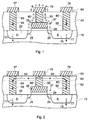
- Figure 1 shows a cross section of a partly finished integrated circuit.
- a semiconductor substrate 10 of a first conductivity type contains source 15 and drain 20 regions of a second conductivity type, opposite to the first.
- Lightly doped drain (LDD) structures 25 may be provided adjacent to the source 15 and drain 20 regions.
- a transistor gate insulator 30 lies on the semiconductor surface, between the source 15 and drain 20.
- a gate electrode 35 lies over the gate insulator 30.
- a first interlevel dielectric layer 40 has been deposited over the structure. Contact holes 45, 50, 55 have been etched through the dielectric layer 40 above drain 20, gate 35, and source 15 regions, respectively. The contact holes are filled with a conductive material 60 according to any suitable process.
- a first interconnect layer 64 has been deposited, and patterned with an etch step to form interconnect wirings 67, 70, 75 in electrical contact with drain 20, gate 35, and source 15 regions, respectively.
- the contact holes 45, 50, 55 and wirings 67, 70, 75 are usually formed by plasma etching, such as reactive ion etching (RIE). During such etch steps, significant electrical charges build up on metallic parts of the structure. When a long wiring has been formed, its entire length acts to collect charge. In a complex integrated circuit, a single wiring may attain a length of several metres.
- plasma etching such as reactive ion etching (RIE).
- any charge that builds up on wirings 67, 75 may be dissipated through the diode junction formed by the substrate 10 and the drain 20 or source 15 regions, respectively. According to the polarity of the charge and the conductivity types of the source, drain and substrate, this dissipation may either be by forward bias conduction of the diode junction, or reverse bias leakage current of the same diode.
- the conduction is represented in the figure by arrows 77.
- the invention provides a method for producing wiring and contacts in an integrated circuit comprising the steps of forming an insulated gate component on a semiconductor substrate, applying a dielectric layer at least partially composed of a photo-reducible material to cover the component, etching holes in the dielectric layer to expose portions of the component, filling the holes with a conductive material to form contact plugs, photo-reducing at least an upper portion of the interlevel dielectric, prior to deposition of the interconnect layer to correspondingly increase its conductivity, covering the resulting structure with an interconnect layer, etching the interconnect layer to define the wiring, the wiring being in electrical contact with the contact plugs, and oxidising the interlevel dielectric to reduce its conductivity.
- One embodiment of the invention includes the step of applying a passivation layer over an upper surface of the structure, the passivation layer being composed of a material opaque to light of the appropriate wavelength, to prevent accidental photo-reduction of the dielectric layers.
- the photo-reducible material is indium oxide
- the photo-reducing step comprises exposing the interlevel dielectric to light of wavelength shorter than 35 ⁇ m.
- the oxidising step comprises exposing the dielectric layer to an ozone containing atmosphere.
- the ozone is produced in situ by exposing oxygen to ultraviolet light.
- the present invention also provides an integrated circuit structure comprising a semiconductor substrate, an interlevel dielectric layer placed on the substrate, contact plugs provided through the dielectric layer, and wiring in electrical contact with the contact plugs, wherein the interlevel dielectric layer is comprised of a photo-reducible material in a low conductivity state.
- interlevel dielectric layers are provided, each having contact plugs therethrough, and each provided with wiring in electrical contact with the contact plugs. At least some of the interlevel dielectric layers include a photo-reducible material in the low conductivity state.
- a surface passivation layer is provided which is opaque to light of the appropriate wavelength, thereby preventing accidental photo-reduction of the material of the dielectric layers.
- indium oxide may be rendered conductive by a process of photo-reduction.
- the materials may be rendered non-conductive again by performing a suitable oxidation step.
- Stoichiometric indium oxide, In 2 O 3 is an insulator, but photo-reduction causes oxygen vacancies and converts the indium oxide into an off-stoichiometric form, InO x (x ⁇ 1.5), which has high conductivity.
- a layer of indium oxide may be produced on a substrate by DC magnetron sputtering, using an indium target in an argon-oxygen plasma containing the substrate, although many other possible techniques exist. Such a layer may form with either an amorphous or a microcrystalline structure. Using sufficient oxygen, this layer may typically be deposited with a conductivity of around 0.1 to 1 S/m. By exposing this layer to a light source of suitable wavelength in an inert atmosphere, photo-reduction takes place. For indium oxide, ultraviolet light of wavelength less than 35 ⁇ m is effective. The conductivity of the layer then rises to approximately 100 to 1000 S/m, which is comparable to the conductivity of a metallic material.
- the layer may be deposited in its reduced form, as oxygen vacancies will naturally exist.
- the conductivity reduces to a low level, typical of stoichiometric In 2 O 3 - about 10 -3 S/m.
- Such oxidation may, for example, be performed in an ozone containing environment by introducing 8 kPa (600 torr) partial pressure of oxygen into a reaction chamber containing the substrate, and illuminating the chamber with the previously described ultraviolet light source.
- 8 kPa (600 torr) partial pressure of oxygen into a reaction chamber containing the substrate, and illuminating the chamber with the previously described ultraviolet light source.
- the indium oxide layer must be shielded from direct exposure to the ultraviolet light. Oxidation takes place, filling the oxygen vacancies, and the indium oxide layer approaches its stoichiometric composition In 2 O 3 and conductivity 10 -3 S/m.
- Crystalline indium oxide has a greater conductivity, but the lowest conductivity that can be achieved with this material is two orders of magnitude greater than that for amorphous or microcrystalline indium oxide.
- Figure 2 shows a cross section of a partially finished integrated circuit embodying a method of the invention.
- the transistor structure 37 is as defined with respect to figure 1.
- an interlevel dielectric 80 composed of a photo-reducible material such as indium oxide has been deposited.
- Contact holes 45, 50, 55 have been cut, and filled with a suitable metallic compound 60, to form plugged contacts.
- this interlevel dielectric 80 is photo-reduced by exposure to light, suitable to render at least the upper surface of it conductive. If the layer 80 is composed of indium oxide, ultraviolet light having a wavelength of less than 35 ⁇ m may be used, at an intensity of 4W.m -2 . After such exposure, at least an upper portion 85 of the interlevel dielectric layer 80 becomes conductive. Interconnect layer 64 is then formed over the interlevel dielectric layer 80.
- This conduction is represented in the figure by arrows 90.
- the source and drain contacts discharge the accumulated charge by conduction 77 through the source and drain junctions, as discussed earlier. Thus, no charge is built up on the gate electrode 35, and no risk of damage to the gate insulator 30 is caused.
- the structure is exposed to the oxidising ambient to render the interlevel dielectric 80 non-conductive once more, over its entire depth. As discussed above, this may be achieved by placing the structure in an oxygen containing atmosphere, and illuminating with the ultraviolet source already mentioned, so long as the structure itself is shielded from the ultraviolet light. This step may be performed in the same chamber as the plasma etching step.
- Figure 3 shows a cross-section of a finished integrated circuit according to the method of the invention.
- Three layers 64, 92, 95 of interconnect are provided, although more are possible.
- a second interlevel dielectric layer 97 is formed between first 64 and second 92 interconnect layers.
- this dielectric layer is at least partially composed of a photo-reducible material, such as indium oxide.
- Contact holes 100 are etched in dielectric layer 97, above wirings 67, 70, 75 of the first interconnect layer 64. These holes are filled with a metallic compound 105 to form plugged vias.
- the structure is subjected to photo-reduction by exposure to the ultraviolet light source in an inert atmosphere to render an upper portion 110 of second interlevel dielectric layer 97 conductive.
- this conductivity allows any charges that build up on the gate electrode 35, 70 to be conducted through the upper portion 110 to source and drain contacts 45, 55, causing no damage to the gate insulator 30.
- This conduction is represented in the figure by arrows 113.
- the structure is then subjected to oxidation, for example by exposure to the ozone containing atmosphere already discussed to render the dielectric 97 non-conductive again over its entire depth. This may be repeated in an identical fashion with third interlevel dielectric layer 115, contact holes 120, metallic compound 125, conductive upper portion 130 of dielectric layer 115, conduction 135 and third interconnect layer 95.
- a passivation layer 140 is applied over the entire surface of the finished integrated circuit.
- this passivation layer is composed of a material opaque to any light which would render dielectric layers 115, 97, 80 conductive. This prevents the dielectric layers from accidentally becoming conductive once again due to incident ultraviolet light.
- a suitable passivation material is silicon nitride.
- the present invention thus achieves its aims, in that charge build up on wirings of the circuit is prevented during the manufacturing of the integrated circuit; no parasitic leakage current flows during operation of the finished integrated circuit, as the dielectric is returned to a non-conductive state before circuit is finished; no lengthy process steps are added by the method of the invention. In effect, only one gas mixture operation and two, very fast, exposures to light are added beyond a normal process flow. Deposition of the photo-reducible dielectric layers of the invention takes the place of deposition of a dielectric layer 40 in known processes.
- indium oxide may be used as a photo-reducible dielectric, such as zinc oxide, titanium oxide, and mixtures of such compounds.
- Each interlevel dielectric layer may be formed from a first sub-layer of a non-photoreducible dielectric, covered in a second sub-layer of a photo-reducible dielectric.
- the invention applies not only to MOS transistors, but also to all semiconductors having at least one isolated electrode, such as double gate EPROM cells.
Landscapes
- Internal Circuitry In Semiconductor Integrated Circuit Devices (AREA)
Applications Claiming Priority (2)
| Application Number | Priority Date | Filing Date | Title |
|---|---|---|---|
| FR9606018 | 1996-05-07 | ||
| FR9606018A FR2748601B1 (fr) | 1996-05-07 | 1996-05-07 | Procede de formation d'interconnexions dans un circuit integre |
Publications (2)
| Publication Number | Publication Date |
|---|---|
| EP0806799A1 true EP0806799A1 (fr) | 1997-11-12 |
| EP0806799B1 EP0806799B1 (fr) | 2004-03-24 |
Family
ID=9492137
Family Applications (1)
| Application Number | Title | Priority Date | Filing Date |
|---|---|---|---|
| EP97410048A Expired - Lifetime EP0806799B1 (fr) | 1996-05-07 | 1997-05-02 | Procédé de formation d'interconnexions dans un circuit intégré |
Country Status (4)
| Country | Link |
|---|---|
| US (2) | US5851919A (fr) |
| EP (1) | EP0806799B1 (fr) |
| DE (1) | DE69728205T2 (fr) |
| FR (1) | FR2748601B1 (fr) |
Cited By (1)
| Publication number | Priority date | Publication date | Assignee | Title |
|---|---|---|---|---|
| WO2007031922A3 (fr) * | 2005-09-15 | 2007-08-30 | Nxp Bv | Structure destinee a un dispositif semi-conducteur et procede de fabrication de celle-ci |
Families Citing this family (11)
| Publication number | Priority date | Publication date | Assignee | Title |
|---|---|---|---|---|
| US6207553B1 (en) * | 1999-01-26 | 2001-03-27 | Advanced Micro Devices, Inc. | Method of forming multiple levels of patterned metallization |
| US7960833B2 (en) * | 2003-10-22 | 2011-06-14 | Marvell World Trade Ltd. | Integrated circuits and interconnect structure for integrated circuits |
| US7851872B2 (en) | 2003-10-22 | 2010-12-14 | Marvell World Trade Ltd. | Efficient transistor structure |
| US7265448B2 (en) * | 2004-01-26 | 2007-09-04 | Marvell World Trade Ltd. | Interconnect structure for power transistors |
| US8319307B1 (en) | 2004-11-19 | 2012-11-27 | Voxtel, Inc. | Active pixel sensors with variable threshold reset |
| US8461628B2 (en) * | 2005-03-18 | 2013-06-11 | Kovio, Inc. | MOS transistor with laser-patterned metal gate, and method for making the same |
| JP5096669B2 (ja) | 2005-07-06 | 2012-12-12 | ルネサスエレクトロニクス株式会社 | 半導体集積回路装置の製造方法 |
| US7425910B1 (en) | 2006-02-27 | 2008-09-16 | Marvell International Ltd. | Transmitter digital-to-analog converter with noise shaping |
| US20140061637A1 (en) * | 2012-08-30 | 2014-03-06 | Jason Gu | Corrosive Resistant Electronic Components |
| KR101936846B1 (ko) * | 2012-10-24 | 2019-01-11 | 에스케이하이닉스 주식회사 | 반도체 소자 및 그 제조방법 |
| CN118471905B (zh) * | 2024-07-10 | 2024-09-27 | 合肥欧益睿芯科技有限公司 | 半导体器件及其制造方法、电子设备 |
Citations (1)
| Publication number | Priority date | Publication date | Assignee | Title |
|---|---|---|---|---|
| EP0072690A2 (fr) * | 1981-08-17 | 1983-02-23 | Fujitsu Limited | Dispositif MIS et procédé pour sa fabrication |
Family Cites Families (6)
| Publication number | Priority date | Publication date | Assignee | Title |
|---|---|---|---|---|
| US3553533A (en) * | 1964-05-14 | 1971-01-05 | Texas Instruments Inc | Dielectric bodies with selectively formed conductive or metallic portions, composites thereof with semiconductor material and methods of making said bodies and composites |
| JPS58207699A (ja) * | 1982-05-28 | 1983-12-03 | 株式会社日立製作所 | 配線回路基板の製造方法 |
| US5459098A (en) * | 1992-10-19 | 1995-10-17 | Marietta Energy Systems, Inc. | Maskless laser writing of microscopic metallic interconnects |
| US5517031A (en) * | 1994-06-21 | 1996-05-14 | General Electric Company | Solid state imager with opaque layer |
| US5559055A (en) * | 1994-12-21 | 1996-09-24 | Advanced Micro Devices, Inc. | Method of decreased interlayer dielectric constant in a multilayer interconnect structure to increase device speed performance |
| US5627094A (en) * | 1995-12-04 | 1997-05-06 | Chartered Semiconductor Manufacturing Pte, Ltd. | Stacked container capacitor using chemical mechanical polishing |
-
1996
- 1996-05-07 FR FR9606018A patent/FR2748601B1/fr not_active Expired - Fee Related
-
1997
- 1997-05-02 EP EP97410048A patent/EP0806799B1/fr not_active Expired - Lifetime
- 1997-05-02 DE DE69728205T patent/DE69728205T2/de not_active Expired - Fee Related
- 1997-05-06 US US08/851,803 patent/US5851919A/en not_active Expired - Lifetime
-
1998
- 1998-07-17 US US09/118,291 patent/US6051884A/en not_active Expired - Lifetime
Patent Citations (1)
| Publication number | Priority date | Publication date | Assignee | Title |
|---|---|---|---|---|
| EP0072690A2 (fr) * | 1981-08-17 | 1983-02-23 | Fujitsu Limited | Dispositif MIS et procédé pour sa fabrication |
Non-Patent Citations (1)
| Title |
|---|
| B.PASHMAKOV ET AL.: "Photoreduction and Oxidation of Amorphous Indium Oxide", SOLID STATE COMMUNICATIONS, vol. 86, no. 10, 1993, G.B., pages 619 - 623, XP002023172 * |
Cited By (2)
| Publication number | Priority date | Publication date | Assignee | Title |
|---|---|---|---|---|
| WO2007031922A3 (fr) * | 2005-09-15 | 2007-08-30 | Nxp Bv | Structure destinee a un dispositif semi-conducteur et procede de fabrication de celle-ci |
| US7928006B2 (en) | 2005-09-15 | 2011-04-19 | Nxp B.V. | Structure for a semiconductor device and a method of manufacturing the same |
Also Published As
| Publication number | Publication date |
|---|---|
| US5851919A (en) | 1998-12-22 |
| EP0806799B1 (fr) | 2004-03-24 |
| DE69728205D1 (de) | 2004-04-29 |
| US6051884A (en) | 2000-04-18 |
| FR2748601A1 (fr) | 1997-11-14 |
| DE69728205T2 (de) | 2005-02-17 |
| FR2748601B1 (fr) | 1998-07-24 |
Similar Documents
| Publication | Publication Date | Title |
|---|---|---|
| US6368939B1 (en) | Multilevel interconnection structure having an air gap between interconnects | |
| KR950011983B1 (ko) | 반도체 장치의 제조방법 | |
| US5010032A (en) | Process for making CMOS device with both P+ and N+ gates including refractory metal silicide and nitride interconnects | |
| US5525837A (en) | Reliable metallization with barrier for semiconductors | |
| EP0119497B1 (fr) | Procédé pour fabriquer des électrodes et bandes d'interconnexion | |
| EP0806799B1 (fr) | Procédé de formation d'interconnexions dans un circuit intégré | |
| US6967363B1 (en) | Lateral diode with multiple spacers | |
| US5811330A (en) | Method of fabricating an overvoltage protection device in integrated circuits | |
| US5843837A (en) | Method of contact hole burying | |
| US6194308B1 (en) | Method of forming wire line | |
| US7271097B2 (en) | Method for manufacturing a semiconductor protection element and a semiconductor device | |
| US4381215A (en) | Method of fabricating a misaligned, composite electrical contact on a semiconductor substrate | |
| US6087238A (en) | Semiconductor device having reduced-width polysilicon gate and non-oxidizing barrier layer and method of manufacture thereof | |
| JP2001313338A (ja) | 半導体装置の製造方法 | |
| KR100237899B1 (ko) | 반도체장치의 제조방법 | |
| US6077771A (en) | Method for forming a barrier layer | |
| KR100461334B1 (ko) | 반도체소자의콘택홀형성방법 | |
| US6563189B1 (en) | Method of adding Zener zap aluminum bridged anti-fuses to a tungsten plug process | |
| JPH10229086A (ja) | 半導体装置およびその製造方法 | |
| US6677207B1 (en) | Vanishingly small integrated circuit diode | |
| KR100284138B1 (ko) | 반도체 소자의 금속 배선 형성 방법 | |
| JP3254549B2 (ja) | 半導体装置及びその製造方法 | |
| US7763951B2 (en) | Fuse structure for maintaining passivation integrity | |
| JP3132480B2 (ja) | 半導体装置の製造方法 | |
| KR100259169B1 (ko) | 반도체 소자 및 그의 제조방법 |
Legal Events
| Date | Code | Title | Description |
|---|---|---|---|
| PUAI | Public reference made under article 153(3) epc to a published international application that has entered the european phase |
Free format text: ORIGINAL CODE: 0009012 |
|
| AK | Designated contracting states |
Kind code of ref document: A1 Designated state(s): DE FR GB IT |
|
| 17P | Request for examination filed |
Effective date: 19980421 |
|
| RAP3 | Party data changed (applicant data changed or rights of an application transferred) |
Owner name: STMICROELECTRONICS S.A. |
|
| RAP1 | Party data changed (applicant data changed or rights of an application transferred) |
Owner name: STMICROELECTRONICS S.A. |
|
| GRAP | Despatch of communication of intention to grant a patent |
Free format text: ORIGINAL CODE: EPIDOSNIGR1 |
|
| GRAS | Grant fee paid |
Free format text: ORIGINAL CODE: EPIDOSNIGR3 |
|
| GRAA | (expected) grant |
Free format text: ORIGINAL CODE: 0009210 |
|
| AK | Designated contracting states |
Kind code of ref document: B1 Designated state(s): DE FR GB IT |
|
| REG | Reference to a national code |
Ref country code: GB Ref legal event code: FG4D |
|
| REF | Corresponds to: |
Ref document number: 69728205 Country of ref document: DE Date of ref document: 20040429 Kind code of ref document: P |
|
| ET | Fr: translation filed | ||
| PLBE | No opposition filed within time limit |
Free format text: ORIGINAL CODE: 0009261 |
|
| STAA | Information on the status of an ep patent application or granted ep patent |
Free format text: STATUS: NO OPPOSITION FILED WITHIN TIME LIMIT |
|
| 26N | No opposition filed |
Effective date: 20041228 |
|
| PGFP | Annual fee paid to national office [announced via postgrant information from national office to epo] |
Ref country code: GB Payment date: 20050427 Year of fee payment: 9 |
|
| PGFP | Annual fee paid to national office [announced via postgrant information from national office to epo] |
Ref country code: DE Payment date: 20050428 Year of fee payment: 9 |
|
| PGFP | Annual fee paid to national office [announced via postgrant information from national office to epo] |
Ref country code: FR Payment date: 20050511 Year of fee payment: 9 |
|
| PG25 | Lapsed in a contracting state [announced via postgrant information from national office to epo] |
Ref country code: GB Free format text: LAPSE BECAUSE OF NON-PAYMENT OF DUE FEES Effective date: 20060502 |
|
| PGFP | Annual fee paid to national office [announced via postgrant information from national office to epo] |
Ref country code: IT Payment date: 20060531 Year of fee payment: 10 |
|
| PG25 | Lapsed in a contracting state [announced via postgrant information from national office to epo] |
Ref country code: DE Free format text: LAPSE BECAUSE OF NON-PAYMENT OF DUE FEES Effective date: 20061201 |
|
| GBPC | Gb: european patent ceased through non-payment of renewal fee |
Effective date: 20060502 |
|
| REG | Reference to a national code |
Ref country code: FR Ref legal event code: ST Effective date: 20070131 |
|
| PG25 | Lapsed in a contracting state [announced via postgrant information from national office to epo] |
Ref country code: FR Free format text: LAPSE BECAUSE OF NON-PAYMENT OF DUE FEES Effective date: 20060531 |
|
| PG25 | Lapsed in a contracting state [announced via postgrant information from national office to epo] |
Ref country code: IT Free format text: LAPSE BECAUSE OF NON-PAYMENT OF DUE FEES Effective date: 20070502 |