EP0806824A2 - Dispositif et méthode pour un modulateur à porte unique avec amplification - Google Patents
Dispositif et méthode pour un modulateur à porte unique avec amplification Download PDFInfo
- Publication number
- EP0806824A2 EP0806824A2 EP97302934A EP97302934A EP0806824A2 EP 0806824 A2 EP0806824 A2 EP 0806824A2 EP 97302934 A EP97302934 A EP 97302934A EP 97302934 A EP97302934 A EP 97302934A EP 0806824 A2 EP0806824 A2 EP 0806824A2
- Authority
- EP
- European Patent Office
- Prior art keywords
- port
- region
- amplification
- input signal
- signal
- Prior art date
- Legal status (The legal status is an assumption and is not a legal conclusion. Google has not performed a legal analysis and makes no representation as to the accuracy of the status listed.)
- Granted
Links
Images

Classifications
-
- H—ELECTRICITY
- H01—ELECTRIC ELEMENTS
- H01S—DEVICES USING THE PROCESS OF LIGHT AMPLIFICATION BY STIMULATED EMISSION OF RADIATION [LASER] TO AMPLIFY OR GENERATE LIGHT; DEVICES USING STIMULATED EMISSION OF ELECTROMAGNETIC RADIATION IN WAVE RANGES OTHER THAN OPTICAL
- H01S5/00—Semiconductor lasers
- H01S5/02—Structural details or components not essential to laser action
- H01S5/026—Monolithically integrated components, e.g. waveguides, monitoring photo-detectors, drivers
- H01S5/0265—Intensity modulators
-
- H—ELECTRICITY
- H01—ELECTRIC ELEMENTS
- H01S—DEVICES USING THE PROCESS OF LIGHT AMPLIFICATION BY STIMULATED EMISSION OF RADIATION [LASER] TO AMPLIFY OR GENERATE LIGHT; DEVICES USING STIMULATED EMISSION OF ELECTROMAGNETIC RADIATION IN WAVE RANGES OTHER THAN OPTICAL
- H01S5/00—Semiconductor lasers
- H01S5/50—Amplifier structures not provided for in groups H01S5/02 - H01S5/30
Definitions
- the present invention relates generally to optical communications systems, and more particularly to optical modulators for use in communications systems using optical fibers.
- Optical modulators have the ability to provide a reliable, cost-effective alternative to laser sources in remote terminals of optical communication networks.
- modulators are particularly attractive in wavelength-division-multiplexed (WDM) systems, where strict requirements on frequency stability generally make laser-based remote terminals impractically expensive.
- WDM wavelength-division-multiplexed
- signals are generated by a light source (usually a laser) at a host terminal and distributed to remote terminals by a power splitter, wavelength router, or other means. These signals are then modulated at the remote terminals and returned to the host terminal either via the same fiber (bi-directional or duplex operation) or via a second, parallel fiber (unidirectional or simplex operation).
- a disadvantage of modulator-based networks is that transmission losses appear twice in the round-trip signal path, thus leading to limited power budgets for broadband systems.
- modulator packaging must minimize critical fiber alignments.
- single-port (reflection-mode) devices are generally preferred over two-port (transmission-mode) devices, wherein these devices should also be tolerant of fiber misalignment.
- Micro-mechanical modulators for example, as described by Goossen et al. in "Silicon Modulator Based on Mechanically-Active Layer with 1 Mb/sec Capability for Fiber-in-the-Loop Applications," IEEE Photonics Technology Lett., vol. 6, pp. 1119-1121, 1994, are single-port, reflective modulators with an acceptable tolerance of fiber misalignment, and offer prospects for the narrowband applications, but are limited in general to bitrates of a few Mb/s.
- Semiconductor Stark-effect modulators have better modulation bandwidth and can be operated in a single-port, normal-incidence package, but they can be undesirably wavelength- and temperature-sensitive.
- a single-port optical modulator apparatus for use in an optical communications system, comprises: an input/output port for receiving a light input signal; a modulation region for modulating said light input signal in response to an electrical drive signal; an amplification region for providing amplification of said light input signal; and a reflector operable to reflect said light input signal back toward said input/output port, whereby an amplified and modulated light signal is output therefrom.
- the apparatus may further include a photodetector for detecting levels of said light input signal.
- the apparatus may further include a phase modulator for modifying the coherence of said light output signal.
- the amplification region may comprise a semiconductor material.
- the modulation region may comprise a semiconductor material.
- the modulation region and amplification region may be combined in a single region, comprising a semiconductor material, wherein modulation and amplification occur together in said semiconductor material in response to said electrical drive signal.
- the apparatus may include a waveguide for directing said light signal.
- the waveguide may be an active semiconductor waveguide, said modulation region and amplification region being combined in said semiconductor waveguide.
- the apparatus may further include a photodetector monolithically integrated with said single region to thereby provide a single section device.
- the apparatus may further include a photodetector comprising another waveguide region electrically isolated from the waveguide of said modulation region and said amplification region.
- the input light signal may propagate perpendicular to the semiconductor layers which compose said modulation and amplification regions.
- the apparatus may further include a partial reflector coupled to the input/output port, operable to increase amplification through multipass operation.
- the modulation region may be an electro-optic modulator, which may be an interferometric device.
- the modulation region may be fabricated in LiNbO3.
- the amplification region may include an amplifying waveguide doped with rare-earth ions, such as erbium.
- the reflector may be a dichroic reflector, further including a pump laser coupled to said reflector for introducing light of a pump wavelength different from a signal wavelength into said waveguide.
- the modulation region may be coupled to said input output/port and said amplification region to said modulation region, or the amplification region may be coupled to said input/output port and said modulation region to said amplification region.
- the single-port optical modulator may be adapted for packaging in a single-port laser package.
- the modulation region may include a thermo-optic modulator, which may be an interferometric device.
- the amplification region may be fabricated in glass material.
- the apparatus may be included in an integrated circuit.
- a method for operating an optical modulator in an optical communications network is as set out in the independent method claim, preferred forms being set out in the dependent claims.
- the present invention is a single-port, reflective, optical modulator with internal amplification.
- the single-port modulator includes a semiconductor waveguide amplifier with a reflector at one end.
- the single-port geometry reduces the high packaging cost associated with two-port modulators, while the internal amplification compensates for network and coupling losses.
- the single-port optical modulator generally includes an input/output port for receiving a light input signal.
- a modulation region for modulating the light input signal in response to an electrical drive signal is included along with an amplification region for providing amplification of the light input signal.
- the modulation region and the amplification region include a waveguide for directing the light input signal.
- a reflector coupled at one end of the waveguide opposite the input/output port is operable to reflect the light input signal back toward the input/output port, wherein an amplified and modulated light signal is output therefrom.
- the single-port optical modulator with amplification include: an electro-optic, interferometric modulator fabricated in LiNbO3 waveguide, with an amplifying region comprised of rare-earth-doped LiNbO3; a thermo-optic, interferometric modulator fabricated in silica or glass, with an amplifying region comprised of rare-earth-doped silica or glass; and a semiconductor amplifier operated with input and output beams perpendicular to the plane of the semiconductor wafer, with or without an index-guiding waveguide.
- an electro-optic, interferometric modulator fabricated in LiNbO3 waveguide with an amplifying region comprised of rare-earth-doped LiNbO3
- a thermo-optic, interferometric modulator fabricated in silica or glass with an amplifying region comprised of rare-earth-doped silica or glass
- a semiconductor amplifier operated with input and output beams perpendicular to the plane of the semiconductor wa
- the optical modulator 10 of the present invention includes a single input/output (VO) port 12 for receiving a light input from, for example, a fiber optic cable and outputting a modulated and amplified light signal.
- the I/O port may be provided with anti-reflection (AR) coatings, buried facets, angled facets, and/or other means to suppress unwanted reflections.
- a modulation or switching region 14 and amplifying region 16 are coupled to the I/O port 12.
- a reflector region 18 is shown adjacent the amplifying region.
- the switching region 14 and amplifying region 16 may be incorporated into a waveguide structure to concentrate and direct the light energy.
- the modulation region may include either amplitude or phase modulation.
- the switching and amplifying functions may be combined in a single region, as will be discussed in greater detail herein.
- the reflector 18 may be constructed to reflect less than 100% of the light, with a photo-receiver 20 located behind the reflector to provide for full integration of terminal functions.
- a partially-transmitting photodetection region may be incorporated between the amplifying region 16 and the reflector 18.
- an embodiment may include a phase modulator or other means for altering the optical path length traversed by the light signal, to provide dithering for control of phase coherence or pulse shape.
- a phase modulator or other means for altering the optical path length traversed by the light signal may be incorporated between the input/output port and the reflector, or may be operatively connected to the amplifying and/or modulating regions via optical waveguide.
- the modulator 30 is a semiconductor laser amplifier modulator.
- an input/output fiber port 32 is coupled to a single-section amplifier/modulator region 34.
- an active semiconductor waveguide 35 coupled to the input/output fiber port 32.
- the semiconductor region would include patterning in order to provide a high refractive index to the waveguide region.
- the amplifier/modulator region 34 of the shown embodiment includes an anti-reflective (AR) coated facet 36 on a side of that region coupled to the input/output fiber 32.
- AR anti-reflective
- a high-reflective (HR) coated facet 38 is included on the opposite side of the amplifier/modulation region 34.
- the AR and HR facet may be composed of a single or multi-layer dielectric coating with thickness and refractive index chosen to provide a desired reflective effect.
- the reflector could be realized as a waveguide reflector such as a waveguide grating, or as a thin mirror inserted into a gap in the waveguide, or as a mirror mounted on the end of the waveguide by a means which allows rapid movement of the mirror to provide phase dithering.
- optical modulation in the amplifier/modulation region 34 is achieved by adjusting the electrical drive signal to control the amplifier gain.
- modulation and amplification occur together in a single waveguide region.
- the electrical drive signal is applied to the active semiconductor waveguide 35 through an electrode 37 or other similar bias provider.
- individual electrical signals may also be applied to multiple electrodes for individual control of multiple separate regions providing gain, modulation, dithering, or other functions.
- the photodetection function can be included in several ways.
- the current flowing through the amplifier/modulator region 34 has a component which is proportional to the input light level, so reception of an incoming optical signal is possible.
- This method may, however, require somewhat sophisticated circuitry to separate the small photocurrent produced by the incoming optical signal from the much stronger outgoing electrical signal applied to the modulator, and noise from the outgoing signal may degrade the sensitivity to the incoming signal.
- a separate photodetector may be used. This detector can be located on either side of the reflector as discussed with respect to FIG. 1.
- a hybrid solution is found in another embodiment of the present invention optical modulator 40 as shown in FIG. 3, combining a single-section amplifier/modulator 44 having an active semiconductor waveguide 42 and a separate photodetector chip 46 in a single package. Like components from the embodiment shown in FIG. 2 are given like numbers in the embodiment of FIG. 3. Adjacent a reflector facet 39 of the amplifier/modulator region 44 is a normal-incidence photodetector 46.
- One or more electrode regions 48 are also included on the photodetector 46 for application of a bias signal thereto and/or extraction of the detected signal.
- This hybrid solution allows individual optimization of the modulator and detector, does not require advanced photonic integration, and could use currently available laser packages designed to hold a back-face monitor diode.
- FIG. 4 there is shown a third embodiment of a single-port optical modulator 50 having internal amplification, which includes a monolithically integrated photodetector region.
- the embodiment of FIG. 4 includes an input/output optical port 32 coupled to an active semiconductor waveguide 42.
- an amplifier/modulation region 52 and photodetector region 56 are included in a single semiconductor chip 54.
- An AR coated facet 58 is included on a first side of the single package device 54 coupled to the input/output fiber and a HR coated facet 60 is included on the opposite side of the device.
- the photodetector region 56 is located adjacent the amplifier/modulation region 52 and before the high reflector coated facet 60.
- electrodes 62, 64 are included in the amplifier/modulation region 52 and the photodetector region 56, respectively, to enable application of a drive signal and the extraction of a detected signal.
- Coherence control for suppression of optical interference in bi-directional links can also be achieved with the semiconductor laser amplifier modulators 34, 52 shown in FIG. 3 and FIG. 4.
- the phase shift imparted to the light signal by the amplifying waveguide varies with the drive signal, so optical phase dither of the outgoing signal can be obtained by dithering the electrical drive signal.
- Control circuits for providing an oscillation of small amplitude to overcome, for example, certain undesirable effects to an output signal are well known devices that accomplish dithering. Since some incidental amplitude modulation will accompany the phase dither, the dither signal must be at a frequency outside the pass band of the receiver.
- FIG. 3 and FIG. 4 resemble certain travelling wave modulators, with the addition of a reflector to achieve single-port operation.
- This addition makes the devices a cost-effective, high-performance option for optical communication networks. Electrical switching of the gain medium yields ample modulation bandwidth and excellent extinction ratio.
- a broad range of operating wavelengths is handled by a single device, as needed for WDM networks.
- the output signal is at substantially the same wavelength as the input signal, so that no optical filter is required to differentiate between output signal and reflected input signal.
- FIG. 5 there is shown a fourth embodiment of a single-port optical modulator 70 with amplification realized in a two-stage dielectric waveguide 71.
- a first stage of the dielectric waveguide, the modulation region 72 is an electro-optic modulator, such as a Mach-Zehnder interferometric device fabricated in LiNbO3 (lithium niobate).
- the modulation region 72 includes a non-amplifying waveguide 73, wherein a signal received through the I/O port 75 is modulated by means of an electrical signal applied to modulator bias electrodes 74 in the modulation region as shown.
- the second stage 76 of the waveguide is an amplifying waveguide 78, such as a LiNbO3 waveguide which has been doped with suitable rare-earth ions, such as erbium ions.
- amplification of the optical signal is accomplished by means of appropriate pumping of the amplification region with light of a certain wavelength.
- a reflector 80 for example, a dichroic reflector, is coupled to the amplification region 76 opposite the receiving end.
- the amplifier would ordinarily be optically pumped, by introducing light of a pump wavelength (different from the signal wavelength) into the amplifier waveguide by means of a pump laser 82 or other light source.
- the pump light may be introduced through the reflector 80 if the reflector is a dichroic mirror which reflects at the signal wavelength and transmits at the pump wavelength.
- alternative means of introducing the pump light might be a waveguide coupler integrated on the modulator chip (not shown in the figure) or a separate device, such as a fused fiber wavelength-division-multiplexing coupler.
- the modulator is shown adjacent to the I/O port and the amplifier is shown adjacent to the reflector, it would be understood by a person skilled in the art that reversed positions, or combination of amplification and modulation functions in a single region may be desirable for some applications.
- the embodiment shown in Fig. 5 can also provide phase dither for suppression of optical interference in bi-directional links. This is achieved by applying a common voltage to the two electrodes 74 to obtain phase modulation while applying a differential voltage between the two contacts for amplitude modulation.
- a directional coupler 86 is also shown in FIG. 5 for receiving a light input and directing it towards the I/O port 75 and/or an optional photodetector 84. The directional coupler 86 is also responsible for directing amplified, modulated light output from the device.
- thermo-optic modulator may be a Mach-Zehnder interferometric device in which the change in path length of one arm is achieved by changing its temperature with a local micro-heater, instead of through the electro-optic effect.
- Thermo-optic modulators are relatively slow, so it may be difficult to obtain phase dither at rates high enough for effective coherence control.
- FIG. 6 there is shown a fifth embodiment of a single-port optical modulator 100 with amplification realized as a vertical-incidence semiconductor amplifier/modulator.
- the amplification and modulation regions are combined into a single region 102, comprising one or more semiconductor layers which produce gain when biased.
- the light signal propagates perpendicular to the semiconductor layers which form the gain region.
- the reflector is composed of a series of semiconductor layers 104, known in the art as a Bragg reflector, which produces a high reflectivity by multiple-beam interference. The distance traversed by the light signal is short, allowing efficient operation without any waveguide, as shown.
- the input/output port 106 shown adjacent the bias electrode 108 is wide and has no waveguide to define a small aperture, so there can be a wide latitude in the positioning of the input fiber 110 or other optics, allowing inexpensive packaging to be used. Alternatively, it may be desirable to combine the Bragg reflector with the amplification and/or modulation regions.
- the short distance traversed by the light signal may limit the gain available per pass. If so, a partial reflector at the input/output port will provide multipass operation to increase the gain to the desired level. Additional layers added to the semiconductor stack, with appropriate additional electrodes, can provide an integrated photodetector.
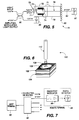
- FIGs. 7 and 8 illustrate some exemplary utilizations for the single-port modulator of the present invention.
- the devices may be included, for example, in a Star network, wherein signals from a host terminal 90 may be routed through a 1 x N splitter 92 or router to a remote terminal 94, where the single-port modulator device 96 is used in bi-directional (duplex) transmission.
- the single port devices may also be used in unidirectional (simplex) transmission between a host terminal 90 and remote terminal 94, as shown in FIG. 8.
- the present invention single-port optical modulator can be packaged in presently available commercial laser packages, achieving significant cost savings both from reduced fiber alignments and from high-volume manufacturing.
- the amplifier gain can be used to overcome coupling losses, thereby improving alignment tolerance, or to add power margin to the network, if desired. If enough amplification is used, the allowed transmission loss of the modulator-based network can be nearly doubled, achieving performance similar to that of a laser-based network.
- Bidirectional transmission in modulator-based networks can suffer from optical interference, however, due to network reflections or Rayleigh scattering, so special measures are needed to control coherence of the upstream and downstream signals.
- provisions for rapid phase dither of the upstream signal might be incorporated into the modulator, as discussed.
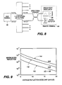
- FIG. 9 shows the level of reflectivity, or maximum end reflection, required at the I/O port for a given reflection-mode gain for a semiconductor laser amplifier. Curves 140, 142 and 144 show required reflectivities for gain ripples of 1-dB, 2-dB and 3-dB, respectively.
Landscapes
- Physics & Mathematics (AREA)
- Condensed Matter Physics & Semiconductors (AREA)
- General Physics & Mathematics (AREA)
- Electromagnetism (AREA)
- Optics & Photonics (AREA)
- Optical Modulation, Optical Deflection, Nonlinear Optics, Optical Demodulation, Optical Logic Elements (AREA)
- Semiconductor Lasers (AREA)
- Lasers (AREA)
- Optical Communication System (AREA)
Applications Claiming Priority (2)
| Application Number | Priority Date | Filing Date | Title |
|---|---|---|---|
| US646169 | 1996-05-07 | ||
| US08/646,169 US5657148A (en) | 1996-05-07 | 1996-05-07 | Apparatus and method for a single-port modulator having amplification |
Publications (3)
| Publication Number | Publication Date |
|---|---|
| EP0806824A2 true EP0806824A2 (fr) | 1997-11-12 |
| EP0806824A3 EP0806824A3 (fr) | 2001-04-25 |
| EP0806824B1 EP0806824B1 (fr) | 2003-06-18 |
Family
ID=24592047
Family Applications (1)
| Application Number | Title | Priority Date | Filing Date |
|---|---|---|---|
| EP97302934A Expired - Lifetime EP0806824B1 (fr) | 1996-05-07 | 1997-04-30 | Dispositif et méthode pour un modulateur à porte unique avec amplification |
Country Status (4)
| Country | Link |
|---|---|
| US (1) | US5657148A (fr) |
| EP (1) | EP0806824B1 (fr) |
| JP (1) | JP3616229B2 (fr) |
| DE (1) | DE69722853T2 (fr) |
Families Citing this family (21)
| Publication number | Priority date | Publication date | Assignee | Title |
|---|---|---|---|---|
| US5784187A (en) * | 1996-07-23 | 1998-07-21 | Lucent Technologies Inc. | Wafer level integration of an optical modulator and III-V photodetector |
| US5966234A (en) * | 1997-06-24 | 1999-10-12 | Lucent Technologies Inc | Retro-reflecting electroabsorption optical modulators |
| US6553043B1 (en) * | 1998-03-02 | 2003-04-22 | Jds Uniphase Corporation | Overcoming L-I kink effects in a laser diode feedback control |
| US6317526B1 (en) * | 1998-12-21 | 2001-11-13 | Fujitsu Limited | Optical phase controller and optical switch |
| EP1059543A1 (fr) * | 1999-05-12 | 2000-12-13 | Hewlett-Packard Company | Appareil de mesure avec une interface optique ayant des faibles pertes dépendant de la polarisation |
| DE19923061A1 (de) * | 1999-05-20 | 2000-11-23 | Bosch Gmbh Robert | Thermooptischer Modulator |
| US6678479B1 (en) | 2000-03-01 | 2004-01-13 | Opnext Japan, Inc. | Semiconductor electro-absorption optical modulator integrated light emission element light emission element module and optical transmission system |
| WO2001061805A1 (fr) * | 2000-02-17 | 2001-08-23 | Nanovation Technologies, Inc. | Amplificateur optique a semi-conducteur et surface emettrice |
| EP1130708B1 (fr) * | 2000-03-02 | 2008-07-16 | OpNext Japan, Inc. | Emetteur de lumiere à semiconducteur intégrant un modulateur electro-absorbant, module et système de transmission optique comprenant cet émetteur |
| US20040028336A1 (en) * | 2001-09-04 | 2004-02-12 | Feuer Mark D. | Method for fabricating optical devices by assembling multiple wafers containing planar optical waveguides |
| WO2002032150A2 (fr) * | 2000-10-12 | 2002-04-18 | Orit Technological R & D Center Ltd. | Dispositif de communication infrarouge, systeme et procede associes |
| JP2002168733A (ja) * | 2000-11-29 | 2002-06-14 | Ando Electric Co Ltd | 光ファイバ波長分散分布測定器及び測定方法 |
| US7065300B1 (en) * | 2000-12-14 | 2006-06-20 | Finsiar Corporation | Optical transmitter including a linear semiconductor optical amplifier |
| US7336414B2 (en) | 2003-06-19 | 2008-02-26 | Nippon Telegraph And Telephone Corporation | Optical modulating device |
| JP2005064051A (ja) * | 2003-08-14 | 2005-03-10 | Fibest Ltd | 光モジュールおよび光通信システム |
| US20050244116A1 (en) * | 2004-04-28 | 2005-11-03 | Evans Alan F | Cables and cable installations |
| US8204384B2 (en) * | 2008-11-21 | 2012-06-19 | Cubic Corporation | Phase-modulating communication device |
| EP2501000A1 (fr) * | 2011-03-14 | 2012-09-19 | Alcatel Lucent | Plage radio étendue utilisant des RSOA à deux sections |
| EP3358685A1 (fr) * | 2017-02-07 | 2018-08-08 | Alcatel Lucent | Émetteur-récepteur auto-injecté pour un réseau optique wdm |
| US11070033B2 (en) * | 2018-02-23 | 2021-07-20 | Nokia Solutions & Networks Oy | Optical amplifier |
| EP3648268A1 (fr) * | 2018-11-02 | 2020-05-06 | Huawei Technologies Co., Ltd. | Dispositif d'amplification optique |
Family Cites Families (9)
| Publication number | Priority date | Publication date | Assignee | Title |
|---|---|---|---|---|
| US3401357A (en) * | 1965-08-11 | 1968-09-10 | Bell Telephone Labor Inc | Electromagnetic wave amplifier oscillator and modulator |
| GB8611241D0 (en) * | 1986-05-08 | 1986-06-18 | British Telecomm | Optical amplifiers |
| JPS63221692A (ja) * | 1987-03-10 | 1988-09-14 | Oki Electric Ind Co Ltd | 半導体光増幅器 |
| LU87164A1 (de) * | 1987-12-15 | 1988-08-23 | Siemens Ag | Reflektionssender fuer ein bidirektionales lwl-kommunikationssystem |
| JP2539089B2 (ja) * | 1990-09-28 | 1996-10-02 | 株式会社東芝 | 半導体レ―ザ増幅器および半導体レ―ザ増幅装置 |
| GB2265059B (en) * | 1992-03-04 | 1995-07-26 | Northern Telecom Ltd | Optical regenerators |
| FR2692374B1 (fr) * | 1992-06-15 | 1994-07-29 | France Telecom | Procede et dispositif de modulation et d'amplification de faisceaux lumineux. |
| US5361157A (en) * | 1992-08-25 | 1994-11-01 | Nippon Hoso Kyokai | Bidirectional light transmission system and optical device therefor |
| US5299057A (en) * | 1992-10-29 | 1994-03-29 | Gte Laboratories Incorporated | Monolithically integrated optical amplifier and photodetector tap |
-
1996
- 1996-05-07 US US08/646,169 patent/US5657148A/en not_active Expired - Lifetime
-
1997
- 1997-04-11 JP JP09337497A patent/JP3616229B2/ja not_active Expired - Fee Related
- 1997-04-30 EP EP97302934A patent/EP0806824B1/fr not_active Expired - Lifetime
- 1997-04-30 DE DE69722853T patent/DE69722853T2/de not_active Expired - Lifetime
Also Published As
| Publication number | Publication date |
|---|---|
| US5657148A (en) | 1997-08-12 |
| JP3616229B2 (ja) | 2005-02-02 |
| EP0806824B1 (fr) | 2003-06-18 |
| DE69722853D1 (de) | 2003-07-24 |
| EP0806824A3 (fr) | 2001-04-25 |
| JPH1039264A (ja) | 1998-02-13 |
| DE69722853T2 (de) | 2004-05-13 |
Similar Documents
| Publication | Publication Date | Title |
|---|---|---|
| EP0806824B1 (fr) | Dispositif et méthode pour un modulateur à porte unique avec amplification | |
| US6577654B1 (en) | Optical signal power monitor and regulator | |
| US11784463B2 (en) | Silicon photonics based tunable laser | |
| US4886334A (en) | Optical amplifying repeater | |
| KR910007710B1 (ko) | 광 증폭기를 이용하는 광파 시스템 | |
| Feuer et al. | Single-port laser-amplifier modulators for local access | |
| JP3262331B2 (ja) | 周波数分割光通信システムのための端子 | |
| EP1121734B1 (fr) | Laser a semi-conducteur et cavite externe activement verrouille en mode multilongueurs d'onde | |
| US6433920B1 (en) | Raman-based utility optical amplifier | |
| JP2957116B2 (ja) | 同調可能なレーザ装置 | |
| CN110459956B (zh) | 一种窄线宽可调谐激光器 | |
| CA2381046A1 (fr) | Laser a cavite externe a verrouillage de longueur d'onde avec modulateur integre | |
| US8213804B2 (en) | Semiconductor optical amplifier for an external cavity diode laser | |
| CN105144509B (zh) | 一种激光器 | |
| US5223972A (en) | Optical amplifiers, optical communication systems networks using the amplifier and integrated optical nodes including the amplifier | |
| JP3044180B2 (ja) | 光周波数トランスレータ | |
| US6327401B1 (en) | Multifrequency laser system | |
| CN108448379A (zh) | 可调谐窄线宽半导体激光器 | |
| JP3269540B2 (ja) | 光増幅器 | |
| JP4022792B2 (ja) | 半導体光増幅装置 | |
| JP2007158057A (ja) | 集積レーザ装置 | |
| Marshall et al. | Optical system with two packaged 1.5 μm semiconductor laser amplifier repeaters | |
| US7110169B1 (en) | Integrated optical device including a vertical lasing semiconductor optical amplifier | |
| US5235604A (en) | Optical amplifier using semiconductor laser as multiplexer | |
| JP4208126B2 (ja) | ゲインクランプ光増幅器モジュール |
Legal Events
| Date | Code | Title | Description |
|---|---|---|---|
| PUAI | Public reference made under article 153(3) epc to a published international application that has entered the european phase |
Free format text: ORIGINAL CODE: 0009012 |
|
| AK | Designated contracting states |
Kind code of ref document: A2 Designated state(s): DE FR GB |
|
| PUAL | Search report despatched |
Free format text: ORIGINAL CODE: 0009013 |
|
| AK | Designated contracting states |
Kind code of ref document: A3 Designated state(s): DE FR GB |
|
| 17P | Request for examination filed |
Effective date: 20011012 |
|
| 17Q | First examination report despatched |
Effective date: 20020225 |
|
| GRAH | Despatch of communication of intention to grant a patent |
Free format text: ORIGINAL CODE: EPIDOS IGRA |
|
| RIC1 | Information provided on ipc code assigned before grant |
Free format text: 7H 01S 5/40 A, 7H 01S 5/02 B, 7H 04B 10/14 B, 7G 02F 1/015 B |
|
| GRAH | Despatch of communication of intention to grant a patent |
Free format text: ORIGINAL CODE: EPIDOS IGRA |
|
| GRAA | (expected) grant |
Free format text: ORIGINAL CODE: 0009210 |
|
| AK | Designated contracting states |
Designated state(s): DE FR GB |
|
| REG | Reference to a national code |
Ref country code: GB Ref legal event code: FG4D |
|
| REF | Corresponds to: |
Ref document number: 69722853 Country of ref document: DE Date of ref document: 20030724 Kind code of ref document: P |
|
| ET | Fr: translation filed | ||
| PLBE | No opposition filed within time limit |
Free format text: ORIGINAL CODE: 0009261 |
|
| STAA | Information on the status of an ep patent application or granted ep patent |
Free format text: STATUS: NO OPPOSITION FILED WITHIN TIME LIMIT |
|
| 26N | No opposition filed |
Effective date: 20040319 |
|
| REG | Reference to a national code |
Ref country code: GB Ref legal event code: 732E Free format text: REGISTERED BETWEEN 20131121 AND 20131127 |
|
| REG | Reference to a national code |
Ref country code: FR Ref legal event code: CD Owner name: ALCATEL-LUCENT USA INC. Effective date: 20131122 |
|
| REG | Reference to a national code |
Ref country code: FR Ref legal event code: GC Effective date: 20140410 |
|
| REG | Reference to a national code |
Ref country code: FR Ref legal event code: RG Effective date: 20141015 |
|
| REG | Reference to a national code |
Ref country code: FR Ref legal event code: PLFP Year of fee payment: 19 |
|
| PGFP | Annual fee paid to national office [announced via postgrant information from national office to epo] |
Ref country code: GB Payment date: 20150420 Year of fee payment: 19 Ref country code: DE Payment date: 20150421 Year of fee payment: 19 |
|
| PGFP | Annual fee paid to national office [announced via postgrant information from national office to epo] |
Ref country code: FR Payment date: 20150421 Year of fee payment: 19 |
|
| REG | Reference to a national code |
Ref country code: DE Ref legal event code: R119 Ref document number: 69722853 Country of ref document: DE |
|
| GBPC | Gb: european patent ceased through non-payment of renewal fee |
Effective date: 20160430 |
|
| REG | Reference to a national code |
Ref country code: FR Ref legal event code: ST Effective date: 20161230 |
|
| PG25 | Lapsed in a contracting state [announced via postgrant information from national office to epo] |
Ref country code: FR Free format text: LAPSE BECAUSE OF NON-PAYMENT OF DUE FEES Effective date: 20160502 Ref country code: GB Free format text: LAPSE BECAUSE OF NON-PAYMENT OF DUE FEES Effective date: 20160430 Ref country code: DE Free format text: LAPSE BECAUSE OF NON-PAYMENT OF DUE FEES Effective date: 20161101 |