EP0806888A1 - Ballast pour une lampe à décharge - Google Patents
Ballast pour une lampe à décharge Download PDFInfo
- Publication number
- EP0806888A1 EP0806888A1 EP97303193A EP97303193A EP0806888A1 EP 0806888 A1 EP0806888 A1 EP 0806888A1 EP 97303193 A EP97303193 A EP 97303193A EP 97303193 A EP97303193 A EP 97303193A EP 0806888 A1 EP0806888 A1 EP 0806888A1
- Authority
- EP
- European Patent Office
- Prior art keywords
- circuit
- signal
- producing
- feedback
- level
- Prior art date
- Legal status (The legal status is an assumption and is not a legal conclusion. Google has not performed a legal analysis and makes no representation as to the accuracy of the status listed.)
- Ceased
Links
- 230000000737 periodic effect Effects 0.000 claims abstract description 22
- 239000004020 conductor Substances 0.000 claims abstract description 12
- 230000004044 response Effects 0.000 claims abstract description 7
- 230000002457 bidirectional effect Effects 0.000 claims abstract description 5
- 230000003750 conditioning effect Effects 0.000 claims abstract description 5
- 239000003990 capacitor Substances 0.000 claims description 16
- 238000006243 chemical reaction Methods 0.000 claims 4
- 239000000872 buffer Substances 0.000 description 4
- 238000010586 diagram Methods 0.000 description 4
- 230000000903 blocking effect Effects 0.000 description 3
- 230000008859 change Effects 0.000 description 3
- 230000009471 action Effects 0.000 description 2
- 230000007423 decrease Effects 0.000 description 2
- 238000012986 modification Methods 0.000 description 2
- 230000004048 modification Effects 0.000 description 2
- 238000006842 Henry reaction Methods 0.000 description 1
- 241000233805 Phoenix Species 0.000 description 1
- 230000001154 acute effect Effects 0.000 description 1
- 238000012937 correction Methods 0.000 description 1
- 230000003247 decreasing effect Effects 0.000 description 1
- 230000003111 delayed effect Effects 0.000 description 1
- 238000013461 design Methods 0.000 description 1
- 238000003780 insertion Methods 0.000 description 1
- 230000037431 insertion Effects 0.000 description 1
- 238000000034 method Methods 0.000 description 1
- 230000001172 regenerating effect Effects 0.000 description 1
- 239000004065 semiconductor Substances 0.000 description 1
- 230000007704 transition Effects 0.000 description 1
- 238000004804 winding Methods 0.000 description 1
Images


Classifications
-
- H—ELECTRICITY
- H05—ELECTRIC TECHNIQUES NOT OTHERWISE PROVIDED FOR
- H05B—ELECTRIC HEATING; ELECTRIC LIGHT SOURCES NOT OTHERWISE PROVIDED FOR; CIRCUIT ARRANGEMENTS FOR ELECTRIC LIGHT SOURCES, IN GENERAL
- H05B41/00—Circuit arrangements or apparatus for igniting or operating discharge lamps
- H05B41/14—Circuit arrangements
- H05B41/36—Controlling
- H05B41/38—Controlling the intensity of light
- H05B41/39—Controlling the intensity of light continuously
- H05B41/392—Controlling the intensity of light continuously using semiconductor devices, e.g. thyristor
- H05B41/3921—Controlling the intensity of light continuously using semiconductor devices, e.g. thyristor with possibility of light intensity variations
- H05B41/3925—Controlling the intensity of light continuously using semiconductor devices, e.g. thyristor with possibility of light intensity variations by frequency variation
-
- H—ELECTRICITY
- H05—ELECTRIC TECHNIQUES NOT OTHERWISE PROVIDED FOR
- H05B—ELECTRIC HEATING; ELECTRIC LIGHT SOURCES NOT OTHERWISE PROVIDED FOR; CIRCUIT ARRANGEMENTS FOR ELECTRIC LIGHT SOURCES, IN GENERAL
- H05B41/00—Circuit arrangements or apparatus for igniting or operating discharge lamps
- H05B41/14—Circuit arrangements
- H05B41/26—Circuit arrangements in which the lamp is fed by power derived from DC by means of a converter, e.g. by high-voltage DC
- H05B41/28—Circuit arrangements in which the lamp is fed by power derived from DC by means of a converter, e.g. by high-voltage DC using static converters
- H05B41/282—Circuit arrangements in which the lamp is fed by power derived from DC by means of a converter, e.g. by high-voltage DC using static converters with semiconductor devices
- H05B41/2825—Circuit arrangements in which the lamp is fed by power derived from DC by means of a converter, e.g. by high-voltage DC using static converters with semiconductor devices by means of a bridge converter in the final stage
- H05B41/2828—Circuit arrangements in which the lamp is fed by power derived from DC by means of a converter, e.g. by high-voltage DC using static converters with semiconductor devices by means of a bridge converter in the final stage using control circuits for the switching elements
-
- Y—GENERAL TAGGING OF NEW TECHNOLOGICAL DEVELOPMENTS; GENERAL TAGGING OF CROSS-SECTIONAL TECHNOLOGIES SPANNING OVER SEVERAL SECTIONS OF THE IPC; TECHNICAL SUBJECTS COVERED BY FORMER USPC CROSS-REFERENCE ART COLLECTIONS [XRACs] AND DIGESTS
- Y02—TECHNOLOGIES OR APPLICATIONS FOR MITIGATION OR ADAPTATION AGAINST CLIMATE CHANGE
- Y02B—CLIMATE CHANGE MITIGATION TECHNOLOGIES RELATED TO BUILDINGS, e.g. HOUSING, HOUSE APPLIANCES OR RELATED END-USER APPLICATIONS
- Y02B20/00—Energy efficient lighting technologies, e.g. halogen lamps or gas discharge lamps
-
- Y—GENERAL TAGGING OF NEW TECHNOLOGICAL DEVELOPMENTS; GENERAL TAGGING OF CROSS-SECTIONAL TECHNOLOGIES SPANNING OVER SEVERAL SECTIONS OF THE IPC; TECHNICAL SUBJECTS COVERED BY FORMER USPC CROSS-REFERENCE ART COLLECTIONS [XRACs] AND DIGESTS
- Y10—TECHNICAL SUBJECTS COVERED BY FORMER USPC
- Y10S—TECHNICAL SUBJECTS COVERED BY FORMER USPC CROSS-REFERENCE ART COLLECTIONS [XRACs] AND DIGESTS
- Y10S315/00—Electric lamp and discharge devices: systems
- Y10S315/07—Starting and control circuits for gas discharge lamp using transistors
Definitions
- the present invention relates to a power supply, or ballast, circuit for a gas discharge lamp. More particularly, it relates to a power supply circuit with plural power switches controlled by a feedback circuit in such manner as to allow a user to dynamically adjust the level of light output by the lamp.
- a gas discharge lamp such as a fluorescent lamp, typically utilizes a power supply, or ballast, circuit to convert an a.c. line voltage to a high frequency a.c. voltage which is impressed across a resonant load circuit containing the gas discharge lamp.
- the resonant load circuit includes a resonant inductor and a resonant capacitor for determining the frequency of resonance of current in the resonant load circuit.
- the power supply circuit includes a series half-bridge d.c.-to-a.c. converter having a pair of power switches that alternately connect one end of the resonant load circuit to a d.c. bus voltage and then to a ground, thereby impressing the mentioned a.c. voltage across the resonant load circuit.
- ballast circuit of the foregoing type is disclosed in co-pending U.S. patent 5,341,068, issued August 23, 1994, entitled “Electronic Ballast Arrangement for a Compact Fluorescent Lamp,” by Louis R. Nerone, the present inventor, and assigned to the present assignee.
- the disclosed ballast circuit utilizes a feedback circuit for controlling the mentioned pair of power switches of the d.c.-to-a.c. converter.
- the feedback circuit operates in response to a feedback signal representing an a.c. current in the resonant load circuit.
- the use of the foregoing circuit for controlling the power switches beneficially results in regenerative, or so-called self-resonant, control of the power switches. Accordingly, the ballast circuit of the foregoing patent application avoids the expense and bulk of extra circuitry for switch control.
- the feedback circuit of the foregoing patent application utilizes a magnetic-core transformer with multiple windings.
- the inclusion of such transformer adds considerable bulk to ballast size, which is an especially acute issue with so-called compact fluorescent lamps having a standard screw-type base for insertion into a conventional incandescent lamp socket.
- a feedback circuit avoiding the use of a magnetic transformer is disclosed in the above cross-referenced application Serial No. (attorney docket no. LD 10606).
- the feedback circuit is of the self-resonant type, and is comprised of components which can be implemented in solid-state form, and the majority of which can be incorporated into an integrated circuit.
- the present invention therefore seeks to provide a ballast circuit for a gas discharge lamp that includes, for controlling a pair of power switches, a self-resonant feedback circuit which allows a user to adjust the output of the lamp during lamp operation.
- the invention also seeks to provide, for a ballast circuit of the foregoing type, a user-selectable setpoint of an output parameter of the lamp at which the lamp will more accurately operate.
- the invention seeks to provide still further, for a ballast circuit of the foregoing type, a self-resonant feedback comprised of components which can be implemented in solid-state form, and the majority of which can be incorporated into an integrated circuit.
- a ballast circuit for a gas discharge lamp comprising: (a) a resonant load circuit incorporating a gas discharge lamp and including first and second resonant impedances whose values determine the operating frequency of said resonant load circuit; (b) a d.c.-to-a.c. converter circuit coupled to said resonant load circuit so as to induce an a.c. current in said resonant load circuit, and comprising first and second switches serially connected between a bus conductor at a d.c.
- a ballast circuit for a gas discharge lamp comprising: (a) a resonant load circuit incorporating a gas discharge lamp and including first and second resonant impedances whose values determine the operating frequency of said resonant load circuit; (b) a d.c.-to-a.c. converter circuit coupled to said resonant load circuit so as to induce an a.c. current in said resonant load circuit, and comprising first and second switches serially connected between a bus conductor at a d.c.
- said bidirectional load current flows: (c) an arrangement for allowing a user to select a setpoint signal during lamp operation that determines the amount of light output by the lamp; and (d) a feedback arrangement for regeneratively controlling said first and second switches; said arrangement including a circuit for sensing a.c. current in said resonant load circuit and producing an a.c. feedback signal in proportion to said a.c. current; a circuit for producing a d.c. feedback signal representing an average value of lamp current; and a circuit for generating an error signal between said setpoint signal and said d.c. feedback signal; said feedback arrangement further including: (i) a comparator circuit for comparing said a.c.
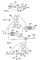
- Fig. 1 is a schematic representation of a ballast circuit for a gas discharge lamp which exclusively uses electronic components in a feedback circuit for implementing self-resonant control of a pair of power switches, and which allows a user to dynamically select a level of light output.
- Fig. 2 shows various voltage waveforms together with state diagrams for the output V o of comparator 31 and of switch 39 of Fig. 1.
- Fig. 3 is a schematic representation of an exemplary implementation of phase splitter, dead time & level shift circuit 50 of Fig. 1.
- Fig. 4 is a schematic representation of an exemplary implementation of dead time circuit 60 of Fig. 3.
- Fig. 5 is a schematic representation of an exemplary implementation of a low pass filter circuit that approximates integrator 37 of Fig. 1.
- an electronic ballast arrangement for a compact fluorescent lamp is effective for converting a standard power line current into a high frequency pulsed signal for driving a compact fluorescent lamp 12.
- the ballast converter circuit 10 receives a d.c. input signal at terminals a-a', which input signal has been derived from an a.c. input power line and has been rectified and, optionally, corrected for power factor by a rectification and power factor correction circuit (not shown).
- ballast circuit 10 The d.c. input signal. received by ballast circuit 10 is coupled across a pair of serially connected power MOSFETs designated Q 1 and Q 2 , which can be provided by International Rectifier of El Segundo, California under the product designation HEXFET MOSFET (HEXFET is a registered trademark of International Rectifier).
- the power MOSFETs Q 1 and Q 2 are effective upon receiving a control signal at their respective gate, or control, terminals thereto (g 1 and g 2 ) for alternately switching between an on and an off condition at a high frequency.
- Node b-b' is a series resonant lamp circuit which consists of the resonant circuit 14, having the inductor and capacitor elements L R and C R selected in size using conventional design means to achieve the desired resonant operating frequency of the lamp 12; capacitor C 2 , which blocks d.c. current from reaching lamp 12; and the lamp 12, which may comprise a compact fluorescent lamp.
- Node b' is also shown as ground 15.
- Self-resonant feedback control of power MOSFET switches Q 1 and Q 2 in Fig. 1 is implemented in Fig. 1 with electronic components, the majority of which can be conveniently incorporated into an integrated circuit for controlling operation of ballast arrangement 10.
- phase control for controlling the alternate switching of MOSFET switches Q 1 and Q 2 is provided by a phase control circuit 30.
- a comparator 31 in circuit 30 receives at its inverting input a feedback voltage V F1 that is proportional to current in lamp 12.
- Shown in dashed lines leading from lamp 12 are alternative conductors 42 and 43. Either one of such conductors is used, the other being omitted.
- Conductor 42 is preferably used for a relatively low d.c. input voltage to circuit 10, e.g. 160 volts, whereas conductor 43 is preferably used for a relatively high d.c. input voltage, e.g. 300 volts.
- Feedback voltage V F1 is derived from the voltage across resistor 44, via a d.c. blocking capacitor 45. Resistor 46 provides a d.c. path to ground 38 from the inverting input of comparator 31.
- Feedback voltage V F1 has an a.c. waveform that typically approximates a sinusoidal waveform, as shown in Fig. 2
- Voltage V F1 is approximately symmetrical about zero-voltage axis, or analog ground 38, and, if necessary, may be provided with a d.c. offset before being input into comparator 31. (Such an offset may typically be required for comparator 31 to properly operate within its input common mode range if incorporated in an integrated circuit having only a single-polarity voltage supply.)
- comparator 31 receives a voltage V +, which is preferably a triangular waveform as shown in Fig. 1.
- Voltage V + is produced in response to a setpoint voltage V S and a feedback voltage V F .
- Setpoint voltage V S is typically proportional to a user-selected value for the amount of light output desired, and could be provided from a rheostat-type control, for instance.
- Feedback voltage V F represents an average value of a lamp output parameter, such as lamp current or lamp lumens. It could, for instance, comprise the same voltage as a.c. feedback signal V F1 that is applied to the inverting input of comparator 31.
- a circuit 32 produces a d.c. feedback voltage V F2 as an average value of feedback voltage V F .
- average is meant herein a d.c. average value such as an r.m.s. value, or a time-averaged value (e.g. during half a cycle of lamp current).
- circuit 32 could comprise an a.c. to r.m.s. converter circuit, or an integrator circuit, both of which are known in the art.
- a summing amplifier 33 receives setpoint voltage V S on its inverting input, and d.c. feedback voltage V F2 on its non-inverting input.
- the error signal produced by summing amplifier 33 is then scaled by a gain factor of G by an amplifier 34, and fed through a p-n, Schottky or other rectifying diode 35.
- the voltage on cathode 36 of diode 35 will have a non-negative value, owing to the diode.
- Such voltage may be as shown in the voltage (V) versus time (T) graph shown in Fig. 1 for a value that is constant for some time.
- the voltage on cathode 36 is received by an non-inverting integrator 37 as a rectangular waveform, as shown in Fig. 1, which is referenced to an analog ground 38.
- Analog ground 38 will usually be different from previously mentioned ground 15 shown beneath transistor Q 1 if the supply voltage (not shown) for phase control circuit 30 is unipolar; if the supply voltage is bipolar, analog ground 38 and ground 15 can be the same.
- Integrator 37 may be approximated by a low pass filter of the resistor-capacitor type, by way of example, as described below (Fig. 5).
- switch 39 Through the switching action of a single-pole, double throw switch 39, integrator 37 is alternately connected directly to p-n diode cathode 36 (via conductor 40) in one switch condition, or connected to cathode 36 through a standard unity-gain inverter 41 in another switch condition.
- Switch 39 may comprise, for instance, an analog switch sold under product designation CD4053 by Harris Semiconductor, of Melbourne, Florida; or, an analog switch sold under product designation MC14053B by Motorola, of Phoenix, Arizona.
- Switch 39 is responsive to output voltage V o of comparator 31 such that, when the comparator output changes state, the switch 36 alternates in its connection to p-n diode cathode 36. This switching action is illustrated in Fig. 2.
- Fig. 2 shows voltage waveforms for comparator input voltages V F1 and V + on the same voltage scale, and shows a d.c. offset voltage, which is assumed the same for both voltages V F1 and V + .
- Fig. 2 also shows a high/low state diagram for comparator output voltage V o , and an up/down state diagram for switch 39 as will be further explained below; these state diagrams have arbitrary vertical scales relative to comparator input voltages V F1 and V + .
- comparator output voltage V o is shown initially as being in a low state.
- switch 39 is connected to conductor 40, which is shown above the switch in Fig. 1 and, during this time, is thus designated as being "UP” in Fig. 2.
- comparator output voltage V o rises to its high state as shown.
- Switch 39 is then connected to unity-gain inverter 41, which shown below the switch in Fig. 1 and, during this time, is thus designated as "DOWN” in Fig. 2.
- comparator output voltage V o switches back to its low state as shown.
- Non-inverting comparator input voltage V + will approximate a triangular waveform where integrator 37 is of the resistive-capacitor type. It is preferred that the upward and downward slopes of voltage V + be fairly linear. This insures at time t, in Fig. 3, for instance, that input voltage V + distinctly surpasses the magnitude of input voltage V F1 so that comparator 31 will reliably change its output state to a low value; if, in contrast, voltage V + rounded off to a more level slope at time t 1 , the desired change of output state of the comparator would be less certain to occur. (The invention would work, however, even if voltage V + is comprised of a predominantly positive-going portion and a predominantly negative-going portion, so long as the following comparator operation occurs.)
- comparator output V o changes from a low level to a high level when input non-inverting input V + exceeds feedback voltage input V F1 , shown at time t 1 in Fig. 2, and changes from a high level to a low level when feedback voltage V F1 exceeds input V + , shown at time t 2 in Fig. 2.
- the output of comparator 31 may be alternatively described as changing levels whenever the absolute value of the a.c. portion of non-inverting voltage V + becomes higher than the absolute value of the a.c.
- Both the waveform for voltage V + and the waveform for feedback voltage V F1 have excursions above an axis of strength that are substantially mirror-images of their excursions below such reference axis, although shifted in time with respect to each other.
- Comparator output voltage V o will typically have a phase advance of, e.g., 20°, to offset the phase delay of, e.g. 20°, occurring in ballast arrangement 10 (Fig. 1) between power switches Q 1 and Q 2 and current-sensing resistor 44. More generally, however, the phase advance of comparator output voltage V o could additionally include 360°, or multiples of 360°, phase advance. Comparator output V o contains the necessary phase information to control operation of power MOSFET switches Q 1 and Q 2 , as will be further described below.
- the power level of lamp 12 can be adjusted by changing the upward and downward slopes of non-inverting voltage V + .
- the comparator output will change earlier, causing the frequency of switching of switches Q 1 and Q 2 to increase, as is apparent from Fig. 2, which decreases the power level of the lamp.
- This can be done by a user decreasing setpoint voltage V s .
- a user would increase setpoint voltage V S , causing the frequency of switching of switches Q 1 and Q 2 to decrease, which increases the power level of the lamp.
- comparator output V o is received by phase splitter, dead time & level shift circuit 50, described below in connection with Fig. 3.
- Circuit 50 provides appropriate signals on lines 50A and 50B that are respectively received by conventional buffers 70 and 72. These buffers are used to drive the gates of MOSFET switches Q 1 and Q 2 with a low impedance.
- Fig. 3 shows an exemplary implementation of phase splitter, dead time & level shift circuit 50 of Fig. 1.
- comparator output voltage V o is applied to a dead time circuit 60, one implementation of which is shown in Fig. 4.
- a circuit comprising resistor 63 and capacitor 65 receives comparator output voltage V o , and provides a delayed input, shown as voltage V 65 , to a logic NOT gate 67.
- Gate 67 is of the type having hysteresis, as indicated by the hysteresis notation in the symbol for gate 67, whereby its input threshold voltage is a function of the state of its output voltage.
- Gate 67 produces an output voltage V 60 , which transitions in the opposite manner from comparator output V o , but only after respective delay (or dead-time) intervals 61.
- a typical delay interval 61 for a lamp operating at a frequency of 50 kilohertz is one microsecond.
- dead-time circuit output voltage V 60 is then input into a logic AND gate 51.
- the other input to gate 51 is the output of logic NOT gate 52, which inverts comparator output V o .
- the output of AND gate 51, voltage V 51 is shown in Fig. 3.
- the output V 51 is then level-shifted by a conventional level shift circuit 54, to provide an appropriate signal on conductor 50A to drive the gate of upper MOSFET Q 1 in Fig. 2 after passing through buffer 70 (Fig. 2).
- a gate-driving voltage V 58 is produced by the circuit of Fig. 3.
- a logic NOT gate 56 first inverts dead-time circuit output V 60 and applies the resulting voltage as one input to logic AND gate 58.
- the other input to AND gate 58 is comparator output voltage V o . Due to the inclusion of NOT gate 56, the gate-driving output voltage V 58 of AND gate 58 appears as shown in the figure, with its phase shifted 180° from the phase of gate-drive signal V 51 . This realizes the phase-splitting function of circuit 50.
- the high states of gate-drive signal V 58 are separated from the high states of gate-drive signal V 51 , on both leading and trailing sides, by dead-time intervals 61. This assures high speed operation of MOSFET switches Q 1 and Q 2 , since so-called soft switching techniques (e.g., zero-voltage switching) can be employed.
- phase splitter, dead time & level shift circuit 50 of Figs. 1 and 3, as well as the function of buffers 70 and 72 in Fig. 1, can be implemented in an obvious manner by those of ordinary skill in the art.
- an IR2155 self-oscillating power MOSFET/IGBT gate driver from International Rectifier of El Segundo, California, could be utilized with the connections illustrated for "bootstrap operation" in its Provisional Data Sheet 6.029, dated January 13, 1994.
- the so-called RT input can be left open, and the present comparator output V o can be applied to the so-called CT input of the gate driver.
- the ability to set the dead time of present dead-time circuit 60 of Figs. 3 and 4 is not present with the use of the foregoing gate driver.
- Fig. 5 shows a low pass filter circuit that approximates integrator 37 of Fig. 1.
- a resistor 80 is connected between the output of analog switch 39 and the non-inverting input of comparator 31.
- a capacitor 81 is connected between the non-inverting input of the comparator and analog ground 38.
- the values of resistor 80 and capacitor 81 are preferably chosen to result in non-inverting input voltage V. (Fig. 2) being approximately linear, for the reasons mentioned above.
- Exemplary circuit values for a circuit for 20-watt fluorescent lamp 12 with an operating current of 50 kilo-hertz, with a d.c. input voltage of 300 volts are as follows: In Fig. 1, resonant inductor L R , 750 micro henries; resonant capacitor C R , 6.8 nanofarads; d.c. blocking capacitor C 2 , 0.47 microfarads; resistor 44, 1.5 ohms; d.c. blocking capacitor 45, 0.5 microfarads; in Fig. 4, resistor 63 and capacitor 65 selected to provide a delay interval 61 of one microsecond; and in Fig. 5, resistor 80, 6.2 k ohms; and capacitor 81, 3.3 nanofarads.
- ballast circuit for a gas discharge lamp that includes, for controlling a pair of power switches, a self-resonant feedback circuit whose components can be implemented in solid-state form, as opposed to the use of a magnetic transformer.
- a user-controllable input is provided to adjust the level of light produced by the lamp.
- the majority of the components of the self-resonant feedback circuit can beneficially be incorporated into an integrated circuit.
- the invention provides a ballast circuit for a gas discharge lamp that includes, for controlling a pair of power switches, a self-resonant feedback circuit which allows a user to adjust the output of the lamp during lamp operation. Additionally, the ballast circuit enables a user to select a setpoint for an output parameter of the lamp at which the lamp will more accurately operate.
- the ballast circuit moreover, includes a self-resonant feedback comprised of components which can be implemented in solid-state form, and the majority of which can be incorporated into an integrated circuit.
Landscapes
- Circuit Arrangements For Discharge Lamps (AREA)
Applications Claiming Priority (2)
| Application Number | Priority Date | Filing Date | Title |
|---|---|---|---|
| US08/644,318 US5717295A (en) | 1996-05-10 | 1996-05-10 | Lamp power supply circuit with feedback circuit for dynamically adjusting lamp current |
| US644318 | 2000-08-23 |
Publications (1)
| Publication Number | Publication Date |
|---|---|
| EP0806888A1 true EP0806888A1 (fr) | 1997-11-12 |
Family
ID=24584390
Family Applications (1)
| Application Number | Title | Priority Date | Filing Date |
|---|---|---|---|
| EP97303193A Ceased EP0806888A1 (fr) | 1996-05-10 | 1997-05-09 | Ballast pour une lampe à décharge |
Country Status (4)
| Country | Link |
|---|---|
| US (1) | US5717295A (fr) |
| EP (1) | EP0806888A1 (fr) |
| JP (1) | JPH1050490A (fr) |
| CN (1) | CN1180987A (fr) |
Cited By (6)
| Publication number | Priority date | Publication date | Assignee | Title |
|---|---|---|---|---|
| EP0831678A2 (fr) * | 1996-09-19 | 1998-03-25 | General Electric Company | Ballast demi-pont à haute tension, commandé par circuit intégré, pour lampe à décharge |
| EP0827370A3 (fr) * | 1996-09-03 | 1998-11-04 | Hitachi, Ltd. | Convertisseur de type resonnant, appareil d'éclairage l'utilisant ainsi que méthode de commande du convertisseur et de l'appareil |
| US6222327B1 (en) | 1996-09-03 | 2001-04-24 | Hitachi, Ltd. | Lighting device for illumination and lamp provided with the same |
| FR2828627A1 (fr) * | 2001-08-10 | 2003-02-14 | Sono Eclair | Dispositif ballast electronique pour maitriser la puissance absorbee par une lampe a decharge, ainsi que le procede mis en oeuvre dans ce dispositif |
| WO2004071136A1 (fr) * | 2003-02-04 | 2004-08-19 | Koninklijke Philips Electronics N.V. | Agencement de circuit |
| RU2314661C1 (ru) * | 2006-04-17 | 2008-01-10 | Открытое акционерное общество ОАО "Орбита" | Задающий генератор устройства управления пускорегулирующего аппарата люминесцентной лампы |
Families Citing this family (20)
| Publication number | Priority date | Publication date | Assignee | Title |
|---|---|---|---|---|
| WO1997027726A1 (fr) * | 1996-01-26 | 1997-07-31 | Tridonic Bauelemente Gmbh | Procede et circuit de commande electronique pour la regulation des caracteristiques de fonctionnement de lampes a decharge |
| JP2972691B2 (ja) * | 1997-02-12 | 1999-11-08 | インターナショナル・レクチファイヤー・コーポレーション | 電子安定器のための位相制御回路 |
| US6008593A (en) * | 1997-02-12 | 1999-12-28 | International Rectifier Corporation | Closed-loop/dimming ballast controller integrated circuits |
| US6300777B1 (en) | 1997-10-15 | 2001-10-09 | International Rectifier Corporation | Lamp ignition detection circuit |
| US6008592A (en) * | 1998-06-10 | 1999-12-28 | International Rectifier Corporation | End of lamp life or false lamp detection circuit for an electronic ballast |
| US6188183B1 (en) | 1998-06-13 | 2001-02-13 | Simon Richard Greenwood | High intensity discharge lamp ballast |
| US6495971B1 (en) | 1998-06-13 | 2002-12-17 | Hatch Transformers, Inc. | High intensity discharge lamp ballast |
| US6204614B1 (en) * | 1999-05-07 | 2001-03-20 | Philips Electronics North America Corporation | Bi-level output electronic high intensity discharge (HID) ballast system |
| JP3322261B2 (ja) * | 2000-03-27 | 2002-09-09 | 松下電器産業株式会社 | 放電ランプ点灯装置 |
| DE60143805D1 (de) * | 2000-10-31 | 2011-02-17 | Osram Sylvania Inc | Ballast-selbstoszillationswechselrichter mit phasengeregelter spannungsrückkopplung |
| EP1579743A1 (fr) * | 2002-12-20 | 2005-09-28 | Koninklijke Philips Electronics N.V. | Mise sous tension a deux etats de lampes hid |
| US7589480B2 (en) * | 2006-05-26 | 2009-09-15 | Greenwood Soar Ip Ltd. | High intensity discharge lamp ballast |
| CN101227781A (zh) * | 2006-08-28 | 2008-07-23 | 亨特风扇公司 | 用于灯具的电流及/或温度控制的系统和方法 |
| CN101175359B (zh) * | 2006-10-30 | 2011-11-30 | 鸿富锦精密工业(深圳)有限公司 | 电子镇流器 |
| US8482213B1 (en) | 2009-06-29 | 2013-07-09 | Panasonic Corporation | Electronic ballast with pulse detection circuit for lamp end of life and output short protection |
| US8344634B2 (en) * | 2010-01-19 | 2013-01-01 | Green Solution Technology Co., Ltd. | Lamp driving apparatus and level shift driving circuit |
| US8947020B1 (en) | 2011-11-17 | 2015-02-03 | Universal Lighting Technologies, Inc. | End of life control for parallel lamp ballast |
| WO2014118658A1 (fr) * | 2013-01-29 | 2014-08-07 | Koninklijke Philips N.V. | Procédé de commande d'un système d'éclairage et système d'éclairage |
| WO2016100567A1 (fr) | 2014-12-16 | 2016-06-23 | Hampton Products International Corporation | Appareil d'éclairage de sécurité |
| CN112688565B (zh) * | 2019-10-18 | 2024-06-11 | 三垦电气株式会社 | 电流谐振电路的控制装置、方法以及电流谐振电源 |
Citations (2)
| Publication number | Priority date | Publication date | Assignee | Title |
|---|---|---|---|---|
| US5329209A (en) * | 1991-12-11 | 1994-07-12 | Marelli Autronica S.P.A. | Self-oscillating circuit for driving a gas discharge lamp, particularly for use on board a motor vehicle |
| US5406177A (en) * | 1994-04-18 | 1995-04-11 | General Electric Company | Gas discharge lamp ballast circuit with compact starting circuit |
Family Cites Families (9)
| Publication number | Priority date | Publication date | Assignee | Title |
|---|---|---|---|---|
| US4251752A (en) * | 1979-05-07 | 1981-02-17 | Synergetics, Inc. | Solid state electronic ballast system for fluorescent lamps |
| US4383203A (en) * | 1981-06-29 | 1983-05-10 | Litek International Inc. | Circuit means for efficiently driving an electrodeless discharge lamp |
| US4523131A (en) * | 1982-12-10 | 1985-06-11 | Honeywell Inc. | Dimmable electronic gas discharge lamp ballast |
| NL8800288A (nl) * | 1988-02-08 | 1989-09-01 | Nedap Nv | Voorschakelapparaat voor een fluorescentielamp. |
| US5075599A (en) * | 1989-11-29 | 1991-12-24 | U.S. Philips Corporation | Circuit arrangement |
| CA2076127A1 (fr) * | 1991-09-26 | 1993-03-27 | Louis R. Nerone | Montage electronique de ballast pour tube fluorescent compact |
| US5363020A (en) * | 1993-02-05 | 1994-11-08 | Systems And Service International, Inc. | Electronic power controller |
| US5414325A (en) * | 1994-04-13 | 1995-05-09 | General Electric Company | Gas discharge lamp ballast circuit with automatically calibrated light feedback control |
| US5550436A (en) * | 1994-09-01 | 1996-08-27 | International Rectifier Corporation | MOS gate driver integrated circuit for ballast circuits |
-
1996
- 1996-05-10 US US08/644,318 patent/US5717295A/en not_active Expired - Fee Related
-
1997
- 1997-05-09 EP EP97303193A patent/EP0806888A1/fr not_active Ceased
- 1997-05-09 JP JP9118535A patent/JPH1050490A/ja not_active Withdrawn
- 1997-05-10 CN CN97113026A patent/CN1180987A/zh active Pending
Patent Citations (2)
| Publication number | Priority date | Publication date | Assignee | Title |
|---|---|---|---|---|
| US5329209A (en) * | 1991-12-11 | 1994-07-12 | Marelli Autronica S.P.A. | Self-oscillating circuit for driving a gas discharge lamp, particularly for use on board a motor vehicle |
| US5406177A (en) * | 1994-04-18 | 1995-04-11 | General Electric Company | Gas discharge lamp ballast circuit with compact starting circuit |
Cited By (9)
| Publication number | Priority date | Publication date | Assignee | Title |
|---|---|---|---|---|
| EP0827370A3 (fr) * | 1996-09-03 | 1998-11-04 | Hitachi, Ltd. | Convertisseur de type resonnant, appareil d'éclairage l'utilisant ainsi que méthode de commande du convertisseur et de l'appareil |
| US5977725A (en) * | 1996-09-03 | 1999-11-02 | Hitachi, Ltd. | Resonance type power converter unit, lighting apparatus for illumination using the same and method for control of the converter unit and lighting apparatus |
| US6222327B1 (en) | 1996-09-03 | 2001-04-24 | Hitachi, Ltd. | Lighting device for illumination and lamp provided with the same |
| EP0831678A2 (fr) * | 1996-09-19 | 1998-03-25 | General Electric Company | Ballast demi-pont à haute tension, commandé par circuit intégré, pour lampe à décharge |
| FR2828627A1 (fr) * | 2001-08-10 | 2003-02-14 | Sono Eclair | Dispositif ballast electronique pour maitriser la puissance absorbee par une lampe a decharge, ainsi que le procede mis en oeuvre dans ce dispositif |
| WO2004071136A1 (fr) * | 2003-02-04 | 2004-08-19 | Koninklijke Philips Electronics N.V. | Agencement de circuit |
| US7259523B2 (en) | 2003-02-04 | 2007-08-21 | Koninklijke Philips Electronics N.V. | Circuit arrangement |
| CN100539800C (zh) * | 2003-02-04 | 2009-09-09 | 皇家飞利浦电子股份有限公司 | 电路装置 |
| RU2314661C1 (ru) * | 2006-04-17 | 2008-01-10 | Открытое акционерное общество ОАО "Орбита" | Задающий генератор устройства управления пускорегулирующего аппарата люминесцентной лампы |
Also Published As
| Publication number | Publication date |
|---|---|
| JPH1050490A (ja) | 1998-02-20 |
| US5717295A (en) | 1998-02-10 |
| CN1180987A (zh) | 1998-05-06 |
Similar Documents
| Publication | Publication Date | Title |
|---|---|---|
| US5717295A (en) | Lamp power supply circuit with feedback circuit for dynamically adjusting lamp current | |
| CN1143606C (zh) | 镇流电路 | |
| US7061189B2 (en) | Electronic ballast | |
| US6184630B1 (en) | Electronic lamp ballast with voltage source power feedback to AC-side | |
| US6495971B1 (en) | High intensity discharge lamp ballast | |
| US5166579A (en) | Discharge lamp operating circuit | |
| US5382882A (en) | Power supply circuit for a gas discharge lamp | |
| EP0479352B1 (fr) | Convertisseur pour lampes à décharge avec possibilités de variation d'intensité lumineuse | |
| US5075602A (en) | Discharge lamp control circuit arrangement | |
| CN1316855C (zh) | 具有sepic变换器的灯运行设备 | |
| JP3851092B2 (ja) | ハーフブリッジ形インバータ回路 | |
| AU2003205038A1 (en) | Drive for a half-bridge inverter | |
| EP0641149B1 (fr) | Régulation de puissance d'un onduleur pour une lampe à décharge | |
| CN1153447A (zh) | 电路装置 | |
| EP1605734B1 (fr) | Ballast electronique | |
| US5729098A (en) | Power supply and electronic ballast with a novel boost converter control circuit | |
| EP0835044A2 (fr) | Ballast avec fonction de préchauffage des cathodes | |
| WO2002075908A1 (fr) | Convertisseur continu-continu . | |
| US6756746B2 (en) | Method of delaying and sequencing the starting of inverters that ballast lamps | |
| JP4491234B2 (ja) | ガス放電ランプを駆動する方法及び装置 | |
| US5703439A (en) | Lamp power supply circuit with electronic feedback circuit for switch control | |
| EP1387489B1 (fr) | Circuit à modulation de largeur d'impulsions et dispositif d'éclairage | |
| JPH07106088A (ja) | 紫外線放射放電灯用電子点灯装置 | |
| US20030052623A1 (en) | Ballast for at least one electric incandescent lamp | |
| WO1997033454A1 (fr) | Ballast electronique destine a une lampe fluorescente compacte |
Legal Events
| Date | Code | Title | Description |
|---|---|---|---|
| PUAI | Public reference made under article 153(3) epc to a published international application that has entered the european phase |
Free format text: ORIGINAL CODE: 0009012 |
|
| AK | Designated contracting states |
Kind code of ref document: A1 Designated state(s): DE FR GB IT |
|
| 17P | Request for examination filed |
Effective date: 19980512 |
|
| GRAG | Despatch of communication of intention to grant |
Free format text: ORIGINAL CODE: EPIDOS AGRA |
|
| RIC1 | Information provided on ipc code assigned before grant |
Free format text: 7H 05B 41/295 A, 7H 05B 41/392 B, 7G 05F 1/70 B |
|
| RIC1 | Information provided on ipc code assigned before grant |
Free format text: 7H 05B 41/295 A, 7H 05B 41/392 B, 7G 05F 1/70 B |
|
| 17Q | First examination report despatched |
Effective date: 20011218 |
|
| STAA | Information on the status of an ep patent application or granted ep patent |
Free format text: STATUS: THE APPLICATION HAS BEEN REFUSED |
|
| 18R | Application refused |
Effective date: 20020614 |