EP0807845B1 - Matrice de commande adressable d'un dispositif d'affichage - Google Patents
Matrice de commande adressable d'un dispositif d'affichage Download PDFInfo
- Publication number
- EP0807845B1 EP0807845B1 EP97303370A EP97303370A EP0807845B1 EP 0807845 B1 EP0807845 B1 EP 0807845B1 EP 97303370 A EP97303370 A EP 97303370A EP 97303370 A EP97303370 A EP 97303370A EP 0807845 B1 EP0807845 B1 EP 0807845B1
- Authority
- EP
- European Patent Office
- Prior art keywords
- electrode
- track
- tracks
- section
- resistance
- Prior art date
- Legal status (The legal status is an assumption and is not a legal conclusion. Google has not performed a legal analysis and makes no representation as to the accuracy of the status listed.)
- Expired - Lifetime
Links
- 239000011159 matrix material Substances 0.000 title claims description 21
- 239000005262 ferroelectric liquid crystals (FLCs) Substances 0.000 claims description 8
- 238000001465 metallisation Methods 0.000 claims description 7
- 239000012780 transparent material Substances 0.000 claims description 6
- 230000005540 biological transmission Effects 0.000 description 10
- 230000000694 effects Effects 0.000 description 9
- 238000010438 heat treatment Methods 0.000 description 9
- 239000003990 capacitor Substances 0.000 description 5
- 239000004973 liquid crystal related substance Substances 0.000 description 5
- 239000000463 material Substances 0.000 description 4
- 239000004990 Smectic liquid crystal Substances 0.000 description 3
- 238000010586 diagram Methods 0.000 description 3
- 239000011521 glass Substances 0.000 description 3
- 239000000758 substrate Substances 0.000 description 3
- 238000007599 discharging Methods 0.000 description 2
- 230000005684 electric field Effects 0.000 description 2
- 230000006870 function Effects 0.000 description 2
- 230000014509 gene expression Effects 0.000 description 2
- VYZAMTAEIAYCRO-UHFFFAOYSA-N Chromium Chemical compound [Cr] VYZAMTAEIAYCRO-UHFFFAOYSA-N 0.000 description 1
- ZOKXTWBITQBERF-UHFFFAOYSA-N Molybdenum Chemical compound [Mo] ZOKXTWBITQBERF-UHFFFAOYSA-N 0.000 description 1
- 239000004411 aluminium Substances 0.000 description 1
- 229910052782 aluminium Inorganic materials 0.000 description 1
- XAGFODPZIPBFFR-UHFFFAOYSA-N aluminium Chemical compound [Al] XAGFODPZIPBFFR-UHFFFAOYSA-N 0.000 description 1
- 238000003491 array Methods 0.000 description 1
- 210000000988 bone and bone Anatomy 0.000 description 1
- 229910052804 chromium Inorganic materials 0.000 description 1
- 239000011651 chromium Substances 0.000 description 1
- 238000010276 construction Methods 0.000 description 1
- AMGQUBHHOARCQH-UHFFFAOYSA-N indium;oxotin Chemical compound [In].[Sn]=O AMGQUBHHOARCQH-UHFFFAOYSA-N 0.000 description 1
- 229910052751 metal Inorganic materials 0.000 description 1
- 239000002184 metal Substances 0.000 description 1
- 230000004048 modification Effects 0.000 description 1
- 238000012986 modification Methods 0.000 description 1
- 229910052750 molybdenum Inorganic materials 0.000 description 1
- 239000011733 molybdenum Substances 0.000 description 1
- 230000009467 reduction Effects 0.000 description 1
- 238000007789 sealing Methods 0.000 description 1
Images

Classifications
-
- G—PHYSICS
- G02—OPTICS
- G02F—OPTICAL DEVICES OR ARRANGEMENTS FOR THE CONTROL OF LIGHT BY MODIFICATION OF THE OPTICAL PROPERTIES OF THE MEDIA OF THE ELEMENTS INVOLVED THEREIN; NON-LINEAR OPTICS; FREQUENCY-CHANGING OF LIGHT; OPTICAL LOGIC ELEMENTS; OPTICAL ANALOGUE/DIGITAL CONVERTERS
- G02F1/00—Devices or arrangements for the control of the intensity, colour, phase, polarisation or direction of light arriving from an independent light source, e.g. switching, gating or modulating; Non-linear optics
- G02F1/01—Devices or arrangements for the control of the intensity, colour, phase, polarisation or direction of light arriving from an independent light source, e.g. switching, gating or modulating; Non-linear optics for the control of the intensity, phase, polarisation or colour
- G02F1/13—Devices or arrangements for the control of the intensity, colour, phase, polarisation or direction of light arriving from an independent light source, e.g. switching, gating or modulating; Non-linear optics for the control of the intensity, phase, polarisation or colour based on liquid crystals, e.g. single liquid crystal display cells
- G02F1/133—Constructional arrangements; Operation of liquid crystal cells; Circuit arrangements
- G02F1/1333—Constructional arrangements; Manufacturing methods
- G02F1/133382—Heating or cooling of liquid crystal cells other than for activation, e.g. circuits or arrangements for temperature control, stabilisation or uniform distribution over the cell
-
- G—PHYSICS
- G02—OPTICS
- G02F—OPTICAL DEVICES OR ARRANGEMENTS FOR THE CONTROL OF LIGHT BY MODIFICATION OF THE OPTICAL PROPERTIES OF THE MEDIA OF THE ELEMENTS INVOLVED THEREIN; NON-LINEAR OPTICS; FREQUENCY-CHANGING OF LIGHT; OPTICAL LOGIC ELEMENTS; OPTICAL ANALOGUE/DIGITAL CONVERTERS
- G02F1/00—Devices or arrangements for the control of the intensity, colour, phase, polarisation or direction of light arriving from an independent light source, e.g. switching, gating or modulating; Non-linear optics
- G02F1/01—Devices or arrangements for the control of the intensity, colour, phase, polarisation or direction of light arriving from an independent light source, e.g. switching, gating or modulating; Non-linear optics for the control of the intensity, phase, polarisation or colour
- G02F1/13—Devices or arrangements for the control of the intensity, colour, phase, polarisation or direction of light arriving from an independent light source, e.g. switching, gating or modulating; Non-linear optics for the control of the intensity, phase, polarisation or colour based on liquid crystals, e.g. single liquid crystal display cells
- G02F1/133—Constructional arrangements; Operation of liquid crystal cells; Circuit arrangements
- G02F1/1333—Constructional arrangements; Manufacturing methods
- G02F1/1343—Electrodes
- G02F1/13439—Electrodes characterised by their electrical, optical, physical properties; materials therefor; method of making
Definitions
- This invention relates to addressable matrix arrays, and is concerned more particularly, but not exclusively, with ferroelectric liquid crystal devices.
- a conventional FLCD cell comprises a layer of ferroelectric smectic liquid crystal material between two parallel glass substrates, electrode structures being typically provided on the inside facing surfaces of the glass substrates in the form of row and column electrode tracks which cross one another to form a matrix array.
- switching pulses are applied to the row and column electrode tracks in order to produce electric fields which switch the molecules within the material between two polar states having different molecular orientations.
- a display element or pixel at the intersection of two electrode tracks may appear dark or light depending on the state to which the molecules of the pixel have previously been switched, as a result of the different light transmitting properties of the two molecular orientations.
- the display panel is addressed on a line-by-line basis by applying data pulses in parallel to the column electrode tracks, each data pulse being either a switching pulse or a non-switching pulse, and by sequentially applying a strobe pulse to the row electrode tracks so as to switch selected pixels along each row from one state to the other under the effect of the electric field produced by the voltage difference between the data pulse and the strobe pulse applied to the relevant electrode tracks.
- a blanking pulse is applied sequentially to the row electrode tracks which is of such a voltage and duration as to set all the pixels along each row to one state, irrespective of the data pulses applied to the column electrode tracks.
- Subsequent application of strobe and data pulses may then be used to switch selected pixels to the other state whilst leaving the remaining pixels in the one state.
- the power loss due to repeated charging and discharging of the liquid crystal capacitance through the electrode tracks, can lead to a large heating effect.
- the image quality and addressing properties of such displays are highly sensitive to temperature, such heating can lead to changes in the display performance. If the temperature increases uniformly over a display panel as a result of this heating effect, then the addressing parameters can be modified, for example by modifying the switching waveforms in dependence on the sensed temperature of the panel, in order to ensure satisfactory display performance.
- Japanese Patent Publication No. 2-67521A discloses a ferroelectric liquid crystal display in which the resistance of the electrodes increases further from the driving source, for example by making each electrode progressively smaller in cross-section, in order to attempt to provide a uniform temperature distribution within the display.
- an addressable matrix array comprising an addressable matrix of switching elements, a first set of electrode tracks on one side of the matrix, and a second set of electrode tracks on the other side of the matrix, the first and second sets of electrode tracks crossing one another at the locations ofthe switching elements and the switching elements being switchable by the application of respective switching waveforms to the first and second sets of electrode tracks, and at least one of the electrode tracks having a resistance which varies along the length of the electrode track in order to provide increased temperature uniformity over the array due to power dissipation during switching by the switching waveforms applied to the electrode tracks, characterised in that the resistance of an intermediate middle section of said at least one electrode track is greater than the resistance of the two end sections of the electrode track.
- Such variation in the resistance of the electrode tracks can be used to produce spatially uniform power dissipation in the array with the result that the temperature, and hence the display performance in the case of a display, can be rendered more uniform over the array.
- the resistance of said at least one electrode track varies along the length of the electrode track by virtue of the fact that at least one section of the electrode track has a greater transverse width than at least one other section of the electrode track.
- the resistance of said at least one electrode track varies along the length of the electrode track by virtue of the fact that at least one section of the electrode track has a greater metallization thickness than at least one other section of the electrode track.
- At least parts of the electrode tracks are made of transparent material.
- said at least one electrode track comprises a main track portion of transparent material and a supplementary track portion of non-transparent material and of a greater conductivity which runs alongside, and is in electrical contract with, the main track portion.
- the resistance of said at least one electrode track varies along the lengths of the electrode track by virtue of the fact that the main track portion and/or the supplementary track portion of at least one section of the electrode track has a greater transverse width than the corresponding portion of at least one other section of the electrode track.
- the resistance of said at least one electrode track varies along the length of the electrode track by virtue of the fact that the main track portion and/or the supplementary track portion of at least one section of the electrode track has a greater metallization thickness than the corresponding portion of at least one other section of the electrode track.
- the matrix array may be a liquid crystal display, a plasma display, an electroluminescent display, or any other form of matrix device incorporating a matrix of pixels addressable by means of first and second sets of electrode tracks.
- the precise function form of the resistance variation needed to ensure substantially uniform power dissipation will depend on the addressing waveforms and the electrode pattern.
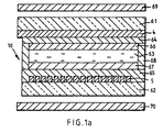
- the FLCD panel 10 comprises a layer 63 of ferroelectric smectic liquid crystal material contained between two parallel glass substrates 61 and 62 bearing first and second electrode structures on their inside surfaces.
- the first and second electrode structures comprise respectively a series of row and column electrode tracks 4 and 5 which cross one another to form a matrix array.
- alignment layers 66 and 67 are provided on insulating layers 64 and 65 applied on top of the row and column electrode tracks 4 and 5, so that the alignment layers 66 and 67 contact opposite sides of the ferroelectric liquid crystal layer 63 which is sealed at its edges by a sealing member 68.
- the panel 10 is disposed between polarisers 69 and 70 having polarising axes which are substantially perpendicular to one another.
- polarisers 69 and 70 having polarising axes which are substantially perpendicular to one another.
- FLCD constitutes only one type of addressable matrix array to which the invention is applicable, and the following description of such a display is therefore to be considered as being given only by way of non-limiting example.
- the FLCD panel can notionally be considered as comprising a network 1 of resistors 2 and capacitors 3, as shown in Figure 1b, the resistors 2 representing the resistance of sections ofthe row and column electrode tracks 4 and 5 provided on either side of the ferroelectric liquid crystal layer and connected to suitable a.c. drive circuitry, and the capacitors 3 representing liquid crystal capacitances of the display pixels at the intersections of the electrode tracks 4 and 5.
- Figure 1b shows only a small portion of the network I and that, in practice, the FLCD panel will incorporate a large number of pixels, for example 1024 X 768, particularly where multiple tracks are required for greyscale addressing by spatial dither or for colour display.
- connection from the row driver circuitry are made to all the row electrode tracks along one edge of the display or connections from the column driver circuitry are made to all the column electrode tracks along a further edge of the display, the heating effect will tend to be greater at locations along the electrode tracks which are closer to the connection points since the power dissipation at such a location will be caused by charging and discharging of the liquid crystal capacitances along the whole of that part of the electrode track which extends from the location away from the connection point, with the result that the panel temperature will tend to be greater over some parts of the panel than over other parts of the panel in operation.
- connection points 11 of a first subset of row electrode tracks at one edge 12 of the panel 10 are made to connection points 13 of a second subset of row electrode tracks at the opposite edge 14 of the panel 10, such that the row electrode tracks of the first subset alternate with the row electrode tracks of the second subset over the panel 10.
- connection points 15 of a first subset of column electrode tracks at a third edge 16 of the panel 10 are made to connection points 17 of a second subset of column electrode tracks at the fourth edge 18 of the panel 10, such that the column electrode tracks of the first subset alternate with the column electrode tracks of the second subset over the panel 10.
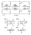
- Figure 3 shows two adjacent column electrode tracks of the panel 10 of Figure 2 modelled as simple transmission lines 30 and 31 and driven by alternating data waveforms applied to opposite ends of the electrode tracks by the column driver circuitry, as indicated by a.c. generators 32 and 33.
- the display pixels are modelled as capacitors 34 and 35 in the transmission lines 30 and 31, and the resistance of the electrode tracks is indicated by distributed resistors R end and R middle , where R end are the resistances of the track sections between adjacent pixels in the vicinity of the two ends of the electrode tracks and R middle are the resistances of the track sections between adjacent pixels in the middle of the electrode tracks.
- the total power dissipated due to Joule heating by the combination of resistances at one end of the transmission lines is approximately (m 2 +1)I 2 R end , where I is the current required to charge/discharge one capacitor (pixel) at the drive frequency and m is the number of capacitances/resistances in each transmission line.
- the total power dissipated by the combination of resistances in the middle of the transmission lines, as circled at (b) in Figure 3 is about 0.5m 2 I 2 R middle .
- each electrode track may be provided by ensuring that each electrode track is thinner in an intermediate middle section of the track than in two end sections of the track, so that it has greater resistivity in the middle section than at the end sections.
- the track resistance may be varied on either or both of the row electrode tracks and column electrode tracks of the panel in order to provide approximately uniform power dissipation, and to thereby ensure as far as possible that the heating effect acts substantially uniformly over the panel so that, if required, known measures can be used to offset the effect on display performance of any temperature variation with time.
- the precise function or form of the resistance variation along each row and/or column electrode track needed to ensure approximately uniform power dissipation over the panel will depend on the addressing waveform and the form of the electrode pattern, including the density and thickness of the electrode tracks.
- FIGS 4 and 5 show sections 41 and 42 of a row electrode track 40 in end and middle regions of the track respectively.
- the electrode track 40 typically comprises a main, relatively narrow transparent portion 43 of indium tin oxide (ITO) and a supplementary, relatively narrow non-transparent portion 44 of a high conductivity metal, such as aluminium, chromium or molybdenum, which runs alongside the portion 43 and is in electrical contact therewith so as to increase the conductivity of the track as a whole.
- the portion 43 crosses the corresponding portion 45 of a column electrode track so as to define a pixel 46 therewith.
- the supplementary portion 44 constitutes a low resistance metallisation strip which serves to improve the conductivity to the drive waveforms (as the ITO portion 43 is of relatively low conductivity) whilst being sufficiently narrow to avoid compromising the light transmitting properties of the panel.
- a comparison of Figures 4 and 5 shows that the supplementary portion 44 is of lesser width, and therefore of greater resistance, in the middle section 42 of Figure 5 than in the end section 41 of Figure 4, whereas the main portion 43 is of the same width in both sections, so that the size of the pixel is the same in both sections.
- the main portion 43 it is also possible for the main portion 43 to be of different widths in the two sections 41 and 42, or for both portions 43 and 44 to be of different widths in the two sections 41 and 42 under certain circumstances.
- the end and middle sections 51 and 52 of an electrode track 50 shown in Figures 6 and 7 comprise a main ITO portion 53 and a supplementary low resistance metallisation portion 54.
- the supplementary portion 54 is of lesser thickness, and therefore of greater resistance, in the middle section 52 of Figure 7 than in the end section 51 of Figure 6, whereas the main portion 53 is of the same thickness in both sections.
- the main portion 53 it is also possible for the main portion 53 to be of lesser thickness in the middle section 52 than in the end section 51, or for both portions 53 and 54 to be of lesser thickness in the middle section 52 than in the end section 51.
- variation in the metallisation thickness of the portion 53 and/or the portion 54 may also be combined with variation of the width of these portions as described with reference to Figures 4 and 5.
- the above described arrangements enable reductions in the non-uniformity of power dissipation, and in corresponding temperature variation, over the panel.
- a spatially uniform display performance may be achieved allowing relatively uniform contrast ratio, greyscale, operating window, viewing angle, etc. in operation of the panel.
Landscapes
- Physics & Mathematics (AREA)
- Nonlinear Science (AREA)
- Mathematical Physics (AREA)
- Chemical & Material Sciences (AREA)
- Crystallography & Structural Chemistry (AREA)
- General Physics & Mathematics (AREA)
- Optics & Photonics (AREA)
- Liquid Crystal (AREA)
- Control Of Indicators Other Than Cathode Ray Tubes (AREA)
- Devices For Indicating Variable Information By Combining Individual Elements (AREA)
- Liquid Crystal Display Device Control (AREA)
Claims (9)
- Matrice de commande adressable comprenant une matrice adressable d'éléments de commutation, un premier ensemble de pistes d'électrodes (4) d'un côté de la matrice et un second ensemble de pistes d'électrodes (5) de l'autre côté de la matrice, les premier et second ensembles de pistes d'électrodes (4,5) se croisant mutuellement aux emplacements des éléments de commutation et les éléments de commutation étant commutables par l'application de formes d'onde de commutation respectives aux premier et second ensembles d'électrodes (4,5), et au moins une des pistes d'électrodes (4,5) ayant une résistance variable dans le sens de la longueur de la piste d'électrode afin d'assurer une uniformité accrue de la température de la matrice du fait de la dissipation d'énergie pendant la commutation effectuée par les formes d'onde de commutation appliquées aux pistes d'électrodes (4,5), caractérisée en ce que la résistance Rintermédiaire d'une section intermédiaire de ladite au moins une piste d'électrode (4,5) est supérieure à la résistance Rextrémité des deux sections d'extrémité de la piste d'électrode.
- Matrice de commande selon la revendication 1, caractérisée en ce que la résistance de ladite au moins une piste d'électrode (4,5) varie dans le sens de la longueur de la piste d'électrode en vertu du fait qu'au moins une section (41) de la piste d'électrode présente une largeur transversale supérieure à au moins une autre section (42) de la piste d'électrode.
- Matrice de commande selon la revendication 1 ou 2, caractérisée en ce que la résistance de ladite au moins une piste d'électrode (4, 5) varie dans le sens de la longueur de métallisation supérieure à au moins une autre section (52) de la piste d'électrode.
- Matrice de commande selon la revendication 1, 2 ou 3, constituant un afficheur matriciel, caractérisée en ce qu'au moins certaines parties (43,53) des pistes d'électrodes (4,5) sont constituées d'un matériau transparent.
- Matrice de commande selon la revendication 4, caractérisée en ce qu'au moins une piste d'électrode (4, 5) comprend une partie de piste principale (43,53) constituée d'un matériau transparent et une partie de piste supplémentaire (44,54) constituée d'un matériau non transparent et de conductivité supérieure, qui se prolonge dans le sens longitudinal de, et en contact électrique avec, la partie de piste principale (43,53).
- Matrice de commande selon la revendication 5, caractérisée en ce que la résistance de ladite au moins une piste d'électrode (4,5) varie dans le sens de la longueur de la piste d'électrode en vertu du fait que la partie de piste principale (43) et/ou la partie de piste supplémentaire (44) d'au moins une section (41) de la piste d'électrode présente une largeur transversale supérieure à la partie correspondante d'au moins une autre section (42) de la piste d'électrode.
- Matrice de commande selon la revendication 5 ou 6, caractérisée en ce que la résistance de ladite au moins une piste d'électrode (4,5) varie dans le sens de la longueur de la piste d'électrode en vertu du fait que la partie de piste principale (53) et/ou la partie de piste supplémentaire (54) d'au moins une section (51) de la piste d'électrode présente une épaisseur de métallisation supérieure à la partie correspondante d'au moins une autre section (52) de la piste d'électrode.
- Matrice de commande selon l'une quelconque des revendications précédentes, caractérisée en ce qu'au moins un des ensembles de pistes d'électrodes (4,5) comprend un premier sous-ensemble de pistes d'électrodes comportant des points de connexion d'extrémité (11) d'un côté (12) de la matrice de commande pour connexion aux circuits d'attaque pour l'application de formes d'onde de commutation respectives aux pistes d'électrodes du premier sous-ensemble au moyen desdits points de connexion d'extrémité (11), et un second sous-ensemble de pistes d'électrodes entrelacées avec les pistes d'électrodes du premier sous-ensemble, comportant des points de connexion d'extrémité (13) du côté opposé (14) de la matrice de commande pour connexion aux circuits d'attaque, permettant d'appliquer des formes d'onde de commutation respectives aux pistes d'électrodes du second sous-ensemble au moyen desdits points de connexion d'extrémité (13).
- Dispositif à cristaux liquides ferroélectriques comportant une matrice de commande conforme à l'une quelconque des revendications précédentes.
Applications Claiming Priority (2)
| Application Number | Priority Date | Filing Date | Title |
|---|---|---|---|
| GB9610322A GB2313226A (en) | 1996-05-17 | 1996-05-17 | Addressable matrix arrays |
| GB9610322 | 1996-05-17 |
Publications (2)
| Publication Number | Publication Date |
|---|---|
| EP0807845A1 EP0807845A1 (fr) | 1997-11-19 |
| EP0807845B1 true EP0807845B1 (fr) | 2004-03-10 |
Family
ID=10793855
Family Applications (1)
| Application Number | Title | Priority Date | Filing Date |
|---|---|---|---|
| EP97303370A Expired - Lifetime EP0807845B1 (fr) | 1996-05-17 | 1997-05-16 | Matrice de commande adressable d'un dispositif d'affichage |
Country Status (5)
| Country | Link |
|---|---|
| US (1) | US5999242A (fr) |
| EP (1) | EP0807845B1 (fr) |
| JP (1) | JPH1048596A (fr) |
| DE (1) | DE69727997T2 (fr) |
| GB (1) | GB2313226A (fr) |
Families Citing this family (9)
| Publication number | Priority date | Publication date | Assignee | Title |
|---|---|---|---|---|
| GB2336931A (en) * | 1998-04-29 | 1999-11-03 | Sharp Kk | Temporal dither addressing scheme for light modulating devices |
| JP4712937B2 (ja) * | 2000-03-27 | 2011-06-29 | エーユー オプトロニクス コーポレイション | 液晶表示装置、配線構造、電圧供給方法およびコンピュータ |
| TW512304B (en) * | 2000-06-13 | 2002-12-01 | Semiconductor Energy Lab | Display device |
| KR100806808B1 (ko) | 2000-10-17 | 2008-02-22 | 엘지.필립스 엘시디 주식회사 | 등저항 배선을 위한 액정표시장치 |
| GB0029315D0 (en) * | 2000-12-01 | 2001-01-17 | Koninkl Philips Electronics Nv | Method of increasing the conductivity of a transparent conductive layer |
| US6750839B1 (en) * | 2002-05-02 | 2004-06-15 | Analog Devices, Inc. | Grayscale reference generator |
| US7420725B2 (en) | 2004-09-27 | 2008-09-02 | Idc, Llc | Device having a conductive light absorbing mask and method for fabricating same |
| US7289259B2 (en) * | 2004-09-27 | 2007-10-30 | Idc, Llc | Conductive bus structure for interferometric modulator array |
| CN104823102B (zh) * | 2012-11-30 | 2018-06-08 | 寇平公司 | 用于显示器加热的电阻器网格 |
Family Cites Families (16)
| Publication number | Priority date | Publication date | Assignee | Title |
|---|---|---|---|---|
| JPS5917430B2 (ja) * | 1977-10-31 | 1984-04-21 | シャープ株式会社 | マトリツクス型液晶表示装置 |
| FR2462755A1 (fr) * | 1979-07-27 | 1981-02-13 | Thomson Csf | Dispositif de visualisation a cristal liquide, et terminal telephonique comportant un tel dispositif |
| US4655561A (en) * | 1983-04-19 | 1987-04-07 | Canon Kabushiki Kaisha | Method of driving optical modulation device using ferroelectric liquid crystal |
| JPS60230632A (ja) * | 1984-04-29 | 1985-11-16 | Casio Comput Co Ltd | 液晶光シャッタ |
| JPS6159425A (ja) * | 1984-08-31 | 1986-03-26 | Canon Inc | 液晶表示素子 |
| US4688896A (en) * | 1985-03-04 | 1987-08-25 | General Electric Company | Information conversion device with auxiliary address lines for enhancing manufacturing yield |
| US4824218A (en) * | 1986-04-09 | 1989-04-25 | Canon Kabushiki Kaisha | Optical modulation apparatus using ferroelectric liquid crystal and low-resistance portions of column electrodes |
| JPH0766253B2 (ja) * | 1986-06-20 | 1995-07-19 | 松下電器産業株式会社 | マトリクス型画像表示装置 |
| JPS6332524A (ja) * | 1986-07-25 | 1988-02-12 | Tokyo Electric Co Ltd | Ohp用熱書込液晶パネル |
| JP2731916B2 (ja) * | 1988-09-02 | 1998-03-25 | キヤノン株式会社 | 強誘電性液晶セル |
| JPH03189622A (ja) * | 1989-12-19 | 1991-08-19 | Citizen Watch Co Ltd | 強誘電性液晶素子 |
| JP2673460B2 (ja) * | 1990-02-26 | 1997-11-05 | キヤノン株式会社 | 液晶表示素子 |
| JPH04269789A (ja) * | 1991-02-25 | 1992-09-25 | Seiko Instr Inc | 電気光学的表示装置 |
| JPH05203997A (ja) * | 1992-01-24 | 1993-08-13 | Toshiba Corp | 液晶表示装置 |
| GB9404356D0 (en) * | 1994-03-07 | 1994-04-20 | Secr Defence | Temperature compensation of ferroelectric liquid crystal displays |
| KR960024595A (ko) * | 1994-12-29 | 1996-07-20 | 윤종용 | 강유전성 액정 표시 소자의 다계조 표시 장치 및 방법 |
-
1996
- 1996-05-17 GB GB9610322A patent/GB2313226A/en not_active Withdrawn
-
1997
- 1997-05-06 US US08/851,616 patent/US5999242A/en not_active Expired - Fee Related
- 1997-05-16 JP JP9127703A patent/JPH1048596A/ja active Pending
- 1997-05-16 DE DE69727997T patent/DE69727997T2/de not_active Expired - Fee Related
- 1997-05-16 EP EP97303370A patent/EP0807845B1/fr not_active Expired - Lifetime
Also Published As
| Publication number | Publication date |
|---|---|
| EP0807845A1 (fr) | 1997-11-19 |
| DE69727997T2 (de) | 2005-02-10 |
| GB9610322D0 (en) | 1996-07-24 |
| GB2313226A (en) | 1997-11-19 |
| US5999242A (en) | 1999-12-07 |
| DE69727997D1 (de) | 2004-04-15 |
| JPH1048596A (ja) | 1998-02-20 |
Similar Documents
| Publication | Publication Date | Title |
|---|---|---|
| EP0592201B1 (fr) | Signaux de commande adaptables pour réduire les effets de couplages parasites dans des structures d'adressage électro-optiques | |
| EP0228557B1 (fr) | Dispositif de modulation optique et sa méthode de commande | |
| EP0224243A2 (fr) | Dispositif de modulation optique et procédé de commande de celui-ci | |
| US5519520A (en) | AC plasma address liquid crystal display | |
| JP2001209063A (ja) | 液晶表示装置およびその表示方法 | |
| EP0807845B1 (fr) | Matrice de commande adressable d'un dispositif d'affichage | |
| KR960014492B1 (ko) | 능동 매트릭스 구동 장치 및 방법 | |
| EP0691639B1 (fr) | Méthode et dispositif de commande d'un panneau d'affichage à cristaux liquides ferro-électriques | |
| KR960008099B1 (ko) | 매트릭스 디스플레이 장치 | |
| US4815823A (en) | Electro-optical device with plural low resistive portions on each high resistive electrode | |
| EP0614168B1 (fr) | Structure d'adressage électro-optique ayant une sensibilité réduite à la diaphonie | |
| KR20080063399A (ko) | 콜레스테릭 액정 표시 장치 | |
| KR100300552B1 (ko) | 광변조장치 | |
| US5719590A (en) | Method for driving an active matrix substrate | |
| KR20040061496A (ko) | 액정 표시 장치 | |
| EP0685832A1 (fr) | Dispositif d'affichage aux cristaux liquides ferroélectriques et méthode de commande permettant d'effectuer un affichage modulable | |
| US5940060A (en) | Ferroelectric liquid crystal cell, method of controlling such a cell, and display | |
| KR100324438B1 (ko) | 액정 디바이스 및 액정 디바이스의 어드레스 방법 | |
| KR100279684B1 (ko) | 액정 디바이스 및 액정 디바이스를 어드레싱하는 방법 | |
| US6046715A (en) | Liquid crystal array device | |
| EP0549337A1 (fr) | Système d'affichage à cristaux liquides | |
| CA1184681A (fr) | Methode d'adressage pour afficheurs a cristaux liquides controles par commutateur | |
| JPH0799415B2 (ja) | 液晶装置 | |
| JPH0869006A (ja) | 電極基板及び液晶素子 | |
| EP0728349A1 (fr) | Compensation de temperature dans l'adressage d'une echelle de gris |
Legal Events
| Date | Code | Title | Description |
|---|---|---|---|
| PUAI | Public reference made under article 153(3) epc to a published international application that has entered the european phase |
Free format text: ORIGINAL CODE: 0009012 |
|
| AK | Designated contracting states |
Kind code of ref document: A1 Designated state(s): DE FR GB |
|
| 17P | Request for examination filed |
Effective date: 19980311 |
|
| 17Q | First examination report despatched |
Effective date: 20020415 |
|
| GRAH | Despatch of communication of intention to grant a patent |
Free format text: ORIGINAL CODE: EPIDOS IGRA |
|
| REG | Reference to a national code |
Ref country code: GB Ref legal event code: FG4D |
|
| GRAS | Grant fee paid |
Free format text: ORIGINAL CODE: EPIDOSNIGR3 |
|
| GRAA | (expected) grant |
Free format text: ORIGINAL CODE: 0009210 |
|
| RAP1 | Party data changed (applicant data changed or rights of an application transferred) |
Owner name: SHARP KABUSHIKI KAISHA |
|
| AK | Designated contracting states |
Kind code of ref document: B1 Designated state(s): DE FR GB |
|
| RAP2 | Party data changed (patent owner data changed or rights of a patent transferred) |
Owner name: SHARP KABUSHIKI KAISHA |
|
| REF | Corresponds to: |
Ref document number: 69727997 Country of ref document: DE Date of ref document: 20040415 Kind code of ref document: P |
|
| ET | Fr: translation filed | ||
| PLBE | No opposition filed within time limit |
Free format text: ORIGINAL CODE: 0009261 |
|
| STAA | Information on the status of an ep patent application or granted ep patent |
Free format text: STATUS: NO OPPOSITION FILED WITHIN TIME LIMIT |
|
| 26N | No opposition filed |
Effective date: 20041213 |
|
| PGFP | Annual fee paid to national office [announced via postgrant information from national office to epo] |
Ref country code: GB Payment date: 20060510 Year of fee payment: 10 |
|
| PGFP | Annual fee paid to national office [announced via postgrant information from national office to epo] |
Ref country code: DE Payment date: 20060524 Year of fee payment: 10 |
|
| PGFP | Annual fee paid to national office [announced via postgrant information from national office to epo] |
Ref country code: FR Payment date: 20060530 Year of fee payment: 10 |
|
| GBPC | Gb: european patent ceased through non-payment of renewal fee |
Effective date: 20070516 |
|
| REG | Reference to a national code |
Ref country code: FR Ref legal event code: ST Effective date: 20080131 |
|
| PG25 | Lapsed in a contracting state [announced via postgrant information from national office to epo] |
Ref country code: DE Free format text: LAPSE BECAUSE OF NON-PAYMENT OF DUE FEES Effective date: 20071201 |
|
| PG25 | Lapsed in a contracting state [announced via postgrant information from national office to epo] |
Ref country code: GB Free format text: LAPSE BECAUSE OF NON-PAYMENT OF DUE FEES Effective date: 20070516 |
|
| PG25 | Lapsed in a contracting state [announced via postgrant information from national office to epo] |
Ref country code: FR Free format text: LAPSE BECAUSE OF NON-PAYMENT OF DUE FEES Effective date: 20070531 |