EP0807974A1 - Mehrschichtige Zwischenverbindungen mit niedriger parasitärer Seitenkapazität - Google Patents
Mehrschichtige Zwischenverbindungen mit niedriger parasitärer Seitenkapazität Download PDFInfo
- Publication number
- EP0807974A1 EP0807974A1 EP97410041A EP97410041A EP0807974A1 EP 0807974 A1 EP0807974 A1 EP 0807974A1 EP 97410041 A EP97410041 A EP 97410041A EP 97410041 A EP97410041 A EP 97410041A EP 0807974 A1 EP0807974 A1 EP 0807974A1
- Authority
- EP
- European Patent Office
- Prior art keywords
- interconnection
- layer
- level
- titanium
- portions
- Prior art date
- Legal status (The legal status is an assumption and is not a legal conclusion. Google has not performed a legal analysis and makes no representation as to the accuracy of the status listed.)
- Ceased
Links
Images
Classifications
-
- H—ELECTRICITY
- H10—SEMICONDUCTOR DEVICES; ELECTRIC SOLID-STATE DEVICES NOT OTHERWISE PROVIDED FOR
- H10W—GENERIC PACKAGES, INTERCONNECTIONS, CONNECTORS OR OTHER CONSTRUCTIONAL DETAILS OF DEVICES COVERED BY CLASS H10
- H10W20/00—Interconnections in chips, wafers or substrates
- H10W20/40—Interconnections external to wafers or substrates, e.g. back-end-of-line [BEOL] metallisations or vias connecting to gate electrodes
- H10W20/41—Interconnections external to wafers or substrates, e.g. back-end-of-line [BEOL] metallisations or vias connecting to gate electrodes characterised by their conductive parts
- H10W20/42—Vias, e.g. via plugs
Definitions
- the present invention relates to the field of semiconductor components and in particular integrated circuits. It relates more particularly to the structure and the manufacture of multilayer connection networks formed on such components.
- level of metallization designates a conductive layer formed at a given stage and appropriately etched
- via designates a passage formed in an insulating layer between two levels of metallization and filled of a conductive material to allow localized connections between portions of two distinct metallization levels.
- the size reductions of integrated circuits make two particular problems linked to more particularly acute connections.
- the first problem resides in the fact that, for large circuits, the stray capacitances between metallization levels are predominant with respect to the lateral capacitances between portions of the same metallization level while this relationship tends to reverse when the miniaturization is increasing.
- the second problem resides in the fact that, as miniaturization increases, the number of components formed in the same silicon chip increases and therefore that the number of connections increases correlatively. As a result, the resistance of the interconnects, the vias and the interconnection / vias interfaces becomes a critical problem, more particularly when it is desired that the integrated circuit can operate at high frequencies.
- an object of the present invention is to provide a new structure and a new method of manufacturing interconnection networks making it possible to overcome the two problems mentioned above.
- Another object of the present invention is to provide a method for manufacturing interconnection levels using essentially individual techniques known in themselves in the field of manufacturing integrated circuits.
- the present invention provides an interconnection structure in which the upper surface of a first interconnection level is a layer of tungsten, portions of the first interconnection level are isolated from each other by an insulator. of the SOG type, portions of a second interconnection level are connected to portions of the first interconnection level by conductive pads formed in openings of an insulating layer of which at least the lower part is of the SOG type, the walls and bottom of said openings are covered with a thin layer of titanium, and the openings are filled with a conductive material selected from the group comprising Al, Cu and aluminum alloys such as alloys of silicon, copper, titanium ...
- a thin layer of TiN is formed under the thin layer of titanium.
- the thickness of the titanium layer is less than 30 nm and preferably less than 10 nm.
- the thickness of the TiN layer is of the order of ten nanometers.
- the present invention also provides a method of forming two levels of an interconnection structure, comprising the steps of forming a first interconnection level of a material chosen from the group comprising Al, Cu and aluminum alloys such than alloys of silicon, copper, titanium, etc., etching this first level of interconnection according to a chosen pattern, covering the structure with an insulating layer, the lower part of which extends between the portions of the first level d interconnection and on the upper surface of the first interconnection level, is made of an SOG type material, etching openings in the insulating layer by looking at selected portions of the first interconnection level, depositing a thin layer of titanium, forming a second interconnection level and filling said openings by deposition at a temperature above 500 ° C. of a material chosen from the group comprising Al, Cu and aluminum alloys.
- this method further comprises the step of depositing on the second interconnection level a thin layer of titanium and a thin layer of tungsten and etching this second interconnection level according to selected patterns.
- a thin layer of TiN is deposited before the thin layer of titanium.
- the thickness of the titanium layer is less than 30 nm and preferably less than 10 nm.
- the thickness of the TiN layer is of the order of ten nanometers.
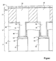
- the single figure is divided vertically into three zones, a zone 1 in which appear portions of a first level of metallization, a zone 2 in which appear portions of a second level of metallization and a zone 3 comprising vias connecting selected portions of the first and second metallization levels.
- first and a second level of metallization this does not mean that the first level of metallization is the lowest level of a interconnection structure.
- This first level can be any intermediate level itself formed above a lower metallization level.
- the assembly between this intermediate level and the lower level will be of the same type as that described here in relation to the first and second metallization levels.
- the first level of metallization 1 two metallization portions 11 and 12 which may be pads, connection lines or portions of connection line. These regions 11 and 12 result from a uniform deposition of a metallization layer followed by etching.
- the first level of metallization is coated with a layer of insulating material which fills the spaces between the portions 11 and 12 and covers the entire structure.
- the height of the conductive portions 11 and 12 can be of the order of 1 ⁇ m while the distance between these portions 11 and 12 can be only of 0.5 ⁇ m. It can therefore be seen that the lateral capacity between these portions is no longer negligible.
- a product as commonly designated in the art by the acronym SOG from the Anglo-Saxon expression Spin On Glass. It is more particularly proposed to use an organic SOG consisting of a polysiloxane added with a diluent (alcohol) which, after annealing, forms an insulator whose dielectric constant is less than 3 and typically with a value of 2 , 6 to 2.8.
- SOG organic SOG consisting of a polysiloxane added with a diluent (alcohol) which, after annealing, forms an insulator whose dielectric constant is less than 3 and typically with a value of 2 , 6 to 2.8.
- the insulators conventionally used in modern technologies are TEOS oxide formed from tetraethylorthosilane whose dielectric constant is 4.4 or an oxide deposited by electronic cyclotron resonance whose dielectric constant is order of 4.
- the SOG layer is formed by spinning the above-mentioned product (polysiloxane plus alcohol) and then annealing at a temperature of 400 to 500 ° C to remove the diluent and polymerize the material which essentially turns into silicon oxide (SiO x ) with added carbon or hydrogen radicals.
- This method has the advantage that it does not involve a step carried out in a plasma for the deposition from which it results that there is no creation of charges inside the insulating layer formed.
- This deposit is also inexpensive and does not require complex equipment.
- SOG as an insulator of an interconnection level is not usual, SOG being generally used in the technique essentially for its planarization capacities. Indeed, after deposition and annealing, the SOG layer has a substantially flat surface.
- the insulating layer of the first interconnection level has been designated by the references 41 and 42.
- the reference 41 designates the SOG layer.
- the SOG has natural planarization qualities, its upper surface is in fact not perfectly flat on the submicron scale. It will therefore be preferable for very small structures to redeposit above the layer of SOG 41 a layer of TEOS 42 and then proceed to a mechanical-chemical planarization step (CMP).
- CMP mechanical-chemical planarization step
- the insulating layer is conventionally etched at the locations where it is desired to form vias.
- the insulating layer is coated with a photosensitive resin which is open at the appropriate locations to provide an etching mask for the insulator.
- the vias 3 are then etched until reaching the upper surface of the targeted portions 11 and 12 of the first interconnection level. After that, the resin is removed to prepare the following steps.
- SOG SOG water molecules and other oxidizing compounds which are then liable to desorb during thermal treatments under vacuum or under plasma and to oxidize visible surfaces or during treatment.
- This polluted area is symbolized in the figure by crosses 43. This is undoubtedly the reason why in the prior art we have avoided using SOG as insulation material and particularly in the areas where vias are formed. .
- a second aspect of the present invention it is intended to use as main constituent materials of the interconnection layers and the vias, highly conductive materials such as aluminum, copper, or aluminum alloys with Cu , Si, Ti ... (for example AlSi, AlSiCu, AlSiTi) by a process avoiding any drawback linked to possible desorptions of oxidizing compounds from the etched parts of a layer of SOG.
- highly conductive materials such as aluminum, copper, or aluminum alloys with Cu , Si, Ti ... (for example AlSi, AlSiCu, AlSiTi)
- the portions 11 and 12 are made of Al, Cu or aluminum alloy.
- the upper surface of each of the portions 11 and 12 is coated with a layer of tungsten, respectively 13 and 14.
- the first metallization level is made of Al or aluminum alloy, it is necessary to provide a layer thin TiN, respectively 15 and 16, between regions 11-13 and 12-14 to avoid the formation of an insulating film resulting from reactions between fluorine and aluminum, the fluorine existing because the deposits of tungsten are made from tungsten fluorides.
- simultaneous deposits are made of a layer of aluminum, copper or aluminum alloy which forms the second interconnection level 2 and the filling 33, 34 of the vias.
- This filling is carried out by a hot deposition technique.
- the deposition is carried out at a plate temperature above 400 ° C. so that the metal flows in the via during the deposition.
- the wettability of the metal along the walls of the via is favored by the titanium sublayer 31.
- TiN titanium nitride
- the metal layer is coated with a layer of tungsten 23 with the interposition of a TiN layer 25.
- the second interconnection level is etched to leave pads or tracks 21, 22 in place by eliminating the parts illustrated in the figure by hatching.
- the present invention has a notable advantage over structures using tungsten for vias or interconnection layers.
- the resistivity of aluminum is around 3 ⁇ / cm while that of tungsten is around 11 ⁇ / cm.
- the barrier and wettability layer 31 can be much thinner than that of the prior art. Indeed, when one wants to burn the second level of interconnection, if this one or the filling of the via is in tungsten, it is necessary to use for engraving a fluorinated plasma. Fluorinated plasma has low selectivity between etching tungsten and etching of the oxide. It is then mandatory that the barrier layer of TiN or Ti / TiN is relatively thick (greater than 100 nm) on the upper surface of the insulating layer 41-42 to allow etching of the second interconnection level to be stopped.
- an aluminum or aluminum alloy layer is etched by a chlorinated plasma which is very selective with respect to the oxide. It is then no longer necessary to provide an etching stop layer and the thickness of the barrier layer 31 is reduced to its minimum to satisfy only its barrier and wettability function and no longer etch stop. Reducing the thickness of these layers is particularly important in practice since the titanium has a resistivity of the order of 13 ⁇ / cm and the TiN of the order of 70 ⁇ / cm. According to the invention, it is possible to use a titanium layer with a thickness of 10 to 30 nm on the flanks of the vias and optionally an underlying layer of TiN with a thickness of the order of 10 nm.
- the present invention using simple techniques which are known in themselves, makes it possible to obtain a significant reduction in the parasitic capacitances and in particular of the lateral parasitic capacitance of the interconnections and of the resistance of the contacts.
Landscapes
- Internal Circuitry In Semiconductor Integrated Circuit Devices (AREA)
- Electrodes Of Semiconductors (AREA)
Applications Claiming Priority (2)
| Application Number | Priority Date | Filing Date | Title |
|---|---|---|---|
| FR9604746 | 1996-04-10 | ||
| FR9604746A FR2747511B1 (fr) | 1996-04-10 | 1996-04-10 | Interconnexions multicouches a faible capacite parasite laterale |
Publications (1)
| Publication Number | Publication Date |
|---|---|
| EP0807974A1 true EP0807974A1 (de) | 1997-11-19 |
Family
ID=9491250
Family Applications (1)
| Application Number | Title | Priority Date | Filing Date |
|---|---|---|---|
| EP97410041A Ceased EP0807974A1 (de) | 1996-04-10 | 1997-04-09 | Mehrschichtige Zwischenverbindungen mit niedriger parasitärer Seitenkapazität |
Country Status (4)
| Country | Link |
|---|---|
| US (1) | US6180520B1 (de) |
| EP (1) | EP0807974A1 (de) |
| JP (1) | JPH1050838A (de) |
| FR (1) | FR2747511B1 (de) |
Families Citing this family (1)
| Publication number | Priority date | Publication date | Assignee | Title |
|---|---|---|---|---|
| US6383951B1 (en) * | 1998-09-03 | 2002-05-07 | Micron Technology, Inc. | Low dielectric constant material for integrated circuit fabrication |
Citations (7)
| Publication number | Priority date | Publication date | Assignee | Title |
|---|---|---|---|---|
| DE4207916A1 (de) * | 1991-04-09 | 1992-10-15 | Mitsubishi Electric Corp | Verbindungsstruktur einer integrierten halbleiterschaltungseinrichtung und verfahren zur herstellung dieser |
| EP0552968A2 (de) * | 1992-01-23 | 1993-07-28 | Samsung Electronics Co. Ltd. | Halbleiteranordnung mit einer Leiterschicht |
| US5328553A (en) * | 1993-02-02 | 1994-07-12 | Motorola Inc. | Method for fabricating a semiconductor device having a planar surface |
| US5399530A (en) * | 1992-06-18 | 1995-03-21 | Sony Corporation | Method of forming interconnection structure to prevent outgassing |
| EP0680085A1 (de) * | 1994-04-28 | 1995-11-02 | Texas Instruments Incorporated | Herstellung von Löchern in polymerischen Materialien |
| US5493152A (en) * | 1993-11-09 | 1996-02-20 | Vlsi Technology, Inc. | Conductive via structure for integrated circuits and method for making same |
| JPH0878520A (ja) * | 1994-08-31 | 1996-03-22 | Fujitsu Ltd | 多層配線を有する半導体装置及びその製造方法 |
Family Cites Families (4)
| Publication number | Priority date | Publication date | Assignee | Title |
|---|---|---|---|---|
| JPS62132359A (ja) * | 1985-12-04 | 1987-06-15 | Fujitsu Ltd | Alメタル層構造 |
| US5635763A (en) * | 1993-03-22 | 1997-06-03 | Sanyo Electric Co., Ltd. | Semiconductor device having cap-metal layer |
| US5360995A (en) * | 1993-09-14 | 1994-11-01 | Texas Instruments Incorporated | Buffered capped interconnect for a semiconductor device |
| US5604155A (en) * | 1995-07-17 | 1997-02-18 | Winbond Electronics Corp. | Al-based contact formation process using Ti glue layer to prevent nodule-induced bridging |
-
1996
- 1996-04-10 FR FR9604746A patent/FR2747511B1/fr not_active Expired - Fee Related
-
1997
- 1997-04-08 US US08/826,921 patent/US6180520B1/en not_active Expired - Lifetime
- 1997-04-09 JP JP9105385A patent/JPH1050838A/ja not_active Withdrawn
- 1997-04-09 EP EP97410041A patent/EP0807974A1/de not_active Ceased
Patent Citations (7)
| Publication number | Priority date | Publication date | Assignee | Title |
|---|---|---|---|---|
| DE4207916A1 (de) * | 1991-04-09 | 1992-10-15 | Mitsubishi Electric Corp | Verbindungsstruktur einer integrierten halbleiterschaltungseinrichtung und verfahren zur herstellung dieser |
| EP0552968A2 (de) * | 1992-01-23 | 1993-07-28 | Samsung Electronics Co. Ltd. | Halbleiteranordnung mit einer Leiterschicht |
| US5399530A (en) * | 1992-06-18 | 1995-03-21 | Sony Corporation | Method of forming interconnection structure to prevent outgassing |
| US5328553A (en) * | 1993-02-02 | 1994-07-12 | Motorola Inc. | Method for fabricating a semiconductor device having a planar surface |
| US5493152A (en) * | 1993-11-09 | 1996-02-20 | Vlsi Technology, Inc. | Conductive via structure for integrated circuits and method for making same |
| EP0680085A1 (de) * | 1994-04-28 | 1995-11-02 | Texas Instruments Incorporated | Herstellung von Löchern in polymerischen Materialien |
| JPH0878520A (ja) * | 1994-08-31 | 1996-03-22 | Fujitsu Ltd | 多層配線を有する半導体装置及びその製造方法 |
Non-Patent Citations (1)
| Title |
|---|
| PATENT ABSTRACTS OF JAPAN vol. 096, no. 007 31 July 1996 (1996-07-31) * |
Also Published As
| Publication number | Publication date |
|---|---|
| FR2747511B1 (fr) | 1998-09-04 |
| FR2747511A1 (fr) | 1997-10-17 |
| JPH1050838A (ja) | 1998-02-20 |
| US6180520B1 (en) | 2001-01-30 |
Similar Documents
| Publication | Publication Date | Title |
|---|---|---|
| EP0351001B1 (de) | Verfahren zur Herstellung einer Halbleitervorrichtung mit mindestens einer kleine Kontaktlöcher enthaltenden Leiterbahn | |
| EP1109221B1 (de) | Damaszene Verbindungsstruktur und ihr Herstellungsverfahren | |
| FR2860920A1 (fr) | Procede de realisation de connexions conductrices de circuits integres, et circuit integre mettant en oeuvre des telles connexions | |
| EP1302954A1 (de) | Herstellungsverfahren eines Induktors und eines Kontaktlochs in einer integrierten Schaltung | |
| JP2001223339A (ja) | 半導体デバイスで用いられるキャパシタとその製造方法 | |
| FR2911432A1 (fr) | Interconnexions d'un circuit electronique integre | |
| FR2754391A1 (fr) | Structure de contact a facteur de forme eleve pour circuits integres | |
| EP0372644B1 (de) | Verfahren zum Herstellen einer integrierten Schaltung einschliesslich Schritte zum Herstellen einer Verbindung zwischen zwei Schichten | |
| FR2813145A1 (fr) | Procede de fabrication d'un condensateur au sein d'un circuit integre, et circuit integre correspondant | |
| FR2774811A1 (fr) | Procede de formation de lignes conductrices sur des circuits integres | |
| EP0892442B1 (de) | Verfahren zur Herstellung einer Metall-Metall-Kapazität in einer integrierten Schaltung und entsprechende integrierte Schaltung | |
| FR2863773A1 (fr) | Procede de fabrication de puces electroniques en silicium aminci | |
| EP0975018B1 (de) | Methode zur Herstellung eines Kondensators in einer integrierten Schaltung | |
| EP0923125A1 (de) | Herstellungsverfahren von metallischen Verbindungen in integrierten Schaltungen | |
| FR2763424A1 (fr) | Processus de damasquinage double | |
| EP0951067B1 (de) | Integrierte Schaltung mit einer Ätz-Stoppschicht und Herstellungsverfahren | |
| EP0807974A1 (de) | Mehrschichtige Zwischenverbindungen mit niedriger parasitärer Seitenkapazität | |
| FR2855324A1 (fr) | Procede de fabrication d'une interconnexion pour un dispositif a semiconducteur | |
| EP0933812B1 (de) | Elektrochemische Abscheidung von Metallen in Halbleiteranordnungen | |
| FR2823377A1 (fr) | Ligne conductrice haute frequence sur un circuit integre | |
| EP1858081A1 (de) | Integrierter Schaltkreis aus Silizium, der in Hyperfrequenz funktioniert, und Verfahren zu dessen Herstellung | |
| KR20010009036A (ko) | 반도체장치의 배선 및 그 연결부 형성방법 | |
| FR2493045A1 (fr) | Structure de capacite dans un circuit integre a deux niveaux de metallisation et procede de fabrication | |
| EP3832707A1 (de) | Verbindungsstruktur eines phasenwechselspeichers | |
| KR100287893B1 (ko) | 반도체소자의제조방법 |
Legal Events
| Date | Code | Title | Description |
|---|---|---|---|
| PUAI | Public reference made under article 153(3) epc to a published international application that has entered the european phase |
Free format text: ORIGINAL CODE: 0009012 |
|
| AK | Designated contracting states |
Kind code of ref document: A1 Designated state(s): DE FR GB IT |
|
| 17P | Request for examination filed |
Effective date: 19980427 |
|
| RAP3 | Party data changed (applicant data changed or rights of an application transferred) |
Owner name: STMICROELECTRONICS S.A. |
|
| 17Q | First examination report despatched |
Effective date: 20011101 |
|
| RAP1 | Party data changed (applicant data changed or rights of an application transferred) |
Owner name: STMICROELECTRONICS S.A. |
|
| STAA | Information on the status of an ep patent application or granted ep patent |
Free format text: STATUS: THE APPLICATION HAS BEEN REFUSED |
|
| 18R | Application refused |
Effective date: 20020706 |