EP0809350A1 - Oscillateur à quartz commandé numériquement et circuit oscillateur intégré monolithique - Google Patents
Oscillateur à quartz commandé numériquement et circuit oscillateur intégré monolithique Download PDFInfo
- Publication number
- EP0809350A1 EP0809350A1 EP97107250A EP97107250A EP0809350A1 EP 0809350 A1 EP0809350 A1 EP 0809350A1 EP 97107250 A EP97107250 A EP 97107250A EP 97107250 A EP97107250 A EP 97107250A EP 0809350 A1 EP0809350 A1 EP 0809350A1
- Authority
- EP
- European Patent Office
- Prior art keywords
- switched
- capacitance
- inverter
- switching
- test
- Prior art date
- Legal status (The legal status is an assumption and is not a legal conclusion. Google has not performed a legal analysis and makes no representation as to the accuracy of the status listed.)
- Granted
Links
- 239000010453 quartz Substances 0.000 title claims description 30
- VYPSYNLAJGMNEJ-UHFFFAOYSA-N silicon dioxide Inorganic materials O=[Si]=O VYPSYNLAJGMNEJ-UHFFFAOYSA-N 0.000 title claims description 30
- 239000013078 crystal Substances 0.000 claims abstract description 23
- 238000012360 testing method Methods 0.000 claims description 47
- 230000000295 complement effect Effects 0.000 claims description 4
- 239000003990 capacitor Substances 0.000 abstract description 11
- 238000005516 engineering process Methods 0.000 abstract description 2
- 230000010355 oscillation Effects 0.000 description 7
- 230000018109 developmental process Effects 0.000 description 2
- 238000010586 diagram Methods 0.000 description 2
- 239000004065 semiconductor Substances 0.000 description 2
- 230000032683 aging Effects 0.000 description 1
- 230000003321 amplification Effects 0.000 description 1
- 230000008878 coupling Effects 0.000 description 1
- 238000010168 coupling process Methods 0.000 description 1
- 238000005859 coupling reaction Methods 0.000 description 1
- 230000001419 dependent effect Effects 0.000 description 1
- 230000002349 favourable effect Effects 0.000 description 1
- 230000001771 impaired effect Effects 0.000 description 1
- 230000007774 longterm Effects 0.000 description 1
- 238000004519 manufacturing process Methods 0.000 description 1
- 238000003199 nucleic acid amplification method Methods 0.000 description 1
- 230000001360 synchronised effect Effects 0.000 description 1
Images

Classifications
-
- H—ELECTRICITY
- H03—ELECTRONIC CIRCUITRY
- H03B—GENERATION OF OSCILLATIONS, DIRECTLY OR BY FREQUENCY-CHANGING, BY CIRCUITS EMPLOYING ACTIVE ELEMENTS WHICH OPERATE IN A NON-SWITCHING MANNER; GENERATION OF NOISE BY SUCH CIRCUITS
- H03B5/00—Generation of oscillations using amplifier with regenerative feedback from output to input
- H03B5/30—Generation of oscillations using amplifier with regenerative feedback from output to input with frequency-determining element being electromechanical resonator
- H03B5/32—Generation of oscillations using amplifier with regenerative feedback from output to input with frequency-determining element being electromechanical resonator being a piezoelectric resonator
- H03B5/36—Generation of oscillations using amplifier with regenerative feedback from output to input with frequency-determining element being electromechanical resonator being a piezoelectric resonator active element in amplifier being semiconductor device
- H03B5/364—Generation of oscillations using amplifier with regenerative feedback from output to input with frequency-determining element being electromechanical resonator being a piezoelectric resonator active element in amplifier being semiconductor device the amplifier comprising field effect transistors
-
- H—ELECTRICITY
- H03—ELECTRONIC CIRCUITRY
- H03B—GENERATION OF OSCILLATIONS, DIRECTLY OR BY FREQUENCY-CHANGING, BY CIRCUITS EMPLOYING ACTIVE ELEMENTS WHICH OPERATE IN A NON-SWITCHING MANNER; GENERATION OF NOISE BY SUCH CIRCUITS
- H03B2201/00—Aspects of oscillators relating to varying the frequency of the oscillations
- H03B2201/02—Varying the frequency of the oscillations by electronic means
- H03B2201/025—Varying the frequency of the oscillations by electronic means the means being an electronic switch for switching in or out oscillator elements
- H03B2201/0266—Varying the frequency of the oscillations by electronic means the means being an electronic switch for switching in or out oscillator elements the means comprising a transistor
Definitions
- Such a quartz oscillator which is operated in a parallel resonance circuit, is known from "Design of quartz oscillators", Bernd Neubig, VHF reports 19 (1979), issues 2 and 3. It is a Pierce oscillator. This can be used to provide a stable frequency for an integrated circuit, which can be changed within a small range due to the switchable frequency setting capacity. Here the high quality of the quartz, its low aging and temperature drift and the high manufacturing accuracy are used to generate stable frequencies.
- the crystal oscillator can be synchronized with a predetermined frequency by switching the capacitances via a control loop (PLL-phase locked loop).
- the feedback resistor R K has a high resistance and serves to set the operating point of the inverter circuit.
- the resistor R behind the output of the inverter circuit is dimensioned so that it ensures a constant amplitude of the oscillator. It depends on the transconductance of the inverter circuit and the size of the frequency setting capacitances C1, C2.
- a disadvantage of this oscillator circuit is that frequency changes are only possible to a small extent. Because with the change in frequency, ie with the change in the frequency setting capacitances C1, C2, the conditions for a stable oscillation of the quartz oscillator change, in particular for a stable frequency and stable Amplitude. Both the requirements for the transconductance of the inverter circuit and for the resistor R connected behind its output change.
- the invention has for its object to provide an oscillator circuit with which a frequency change in a larger range is possible.
- the inverter circuit comprises parallel inverter stages, the first capacitance parallel capacitor stages and the second capacitor C1, C2 each have second parallel capacitor stages, and switching elements are provided such that one inverter stage and one first and a second capacitance level can be switched on or off simultaneously with a control signal.
- an inverter stage contains two amplifier transistors of opposite conductivity type, each connected in series and each connected to a fixed potential, with each of which a switching transistor of the same conductivity type acting as a switching element is connected in series.
- the first capacitance stage is connected to the gate electrodes of the amplifier transistors via a switching element.
- the second capacitance stage is connected to the resistor R via a second switching element.
- the resistance R is selected depending on the size of the transconductance of the inverter stage so that a constant amplitude of the oscillator oscillation is achieved.
- the transconductance of the inverter stage is determined by the dimensioning of the amplifier transistors. It is advantageous to design the amplifier transistors and the switching transistors as CMOS transistors.
- a further test switching transistor of the same conductivity type is connected in series with the amplifier transistor and the switching transistor of a conductivity type in the inverter stages, and a test signal source is arranged in such a way that the switching transistors in the conductive or non-conductive are switched with a test signal supplied by the latter State can be switched, and at the same time the feedback resistor R K can be switched on or off via test switching medium.
- the quartz oscillator can optionally be switched with the test signal into a normal state in which the quartz oscillator oscillates and into a test state.
- the test switching transistors are switched from the test signal to the conductive state and the feedback resistor is switched on, so that the quartz oscillator oscillates at its resonant frequency.
- the switching transistors are switched to the non-conductive state with the test signal, and the feedback resistor is switched off.
- the respective inverter stage is de-energized and the feedback is interrupted.
- the capacities of the various inverter stages can be switched on via the associated switching elements.
- this connection is made via the feedback branch with the coupling resistor R K , so that the current would flow in the entire oscillator circuit. Because it can be tested whether the capacitors have leakage currents or not, it is possible to determine in the test state whether the crystal oscillator meets the requirements specified by the user and the manufacturer. Long-term leakage current freedom is required for many applications. Thus, based on the examinations in the test state, the oscillator circuits which meet or fail to meet the requirements can be determined and sorted out. The leakage currents can be caused in particular by poor oxide properties of the oxide between the capacitor plates. The leakage current can be at a certain voltage and at a certain Temperature are checked, from which it can be concluded that there is no leakage current for a long time under normal conditions.
- the feedback resistor R K can advantageously comprise complementary transistors acting as test switching means, the gate electrodes of which are connected to the test signal source. As a result, the feedback resistor can be easily switched on and off by switching the transistors with the test signal supplied by the test signal source.
- test switching transistors are each connected between the amplifier transistor and the switching transistor. Then the switching transistors at the output of the respective inverter stage in their switched-off state form a high-resistance, so that the gate capacitance of the test switching transistors does not enter into the frequency setting capacitance C1, C2 connected in parallel. In the conductive state, the gate capacitance is formed by the capacitance between the gate electrode and the existing channel between the drain and source zone. Since the test switching transistors are always conductive in the normal state of the quartz oscillator, they also always have a gate capacitance in the normal state.
- the resistor R comprises partial resistors, one of which is connected behind the output of one or more inverter stages. Since the resistor R ensures a constant amplitude of the oscillation, it has to be adapted accordingly in the event of a strong frequency change, which arises through the connection of different capacitances. Depending on how much the capacitance is changed by adding individual stages, a partial resistor R i can be connected behind the output of each inverter stage or behind the output of a group of inverter stages.
- the number of the first and the number of the second capacitance stages is in each case greater than the number of the inverter stages, and switching elements are provided such that a first and a second capacity level can be switched on or off with a control signal.
- a suitable number of capacity levels can thus also be switched on or off without inverter levels. This makes sense for the frequency ranges in which the stability of the oscillator oscillation is not undesirably impaired by a change in capacitance. Capacity levels with and without inverter level can be switched on or off alternately.
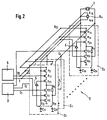
- the oscillator circuit 2 is integrated on a semiconductor chip using CMOS technology.
- the quartz crystal 1 is located outside the semiconductor chip.
- n basic cells Z 1 ... Z n In parallel with the quartz crystal 1 are n basic cells Z 1 ... Z n , to which in turn a feedback resistor R K is connected in parallel.
- Each of the basic cells Z i comprises two capacitances C 1i , C 2i , which are connected in parallel to the quartz 1, one connection being connected to the ground potential.
- each basic cell Z i contains an inverter stage connected in parallel with the quartz 1, two series-connected amplifier transistors p 1i , n 1i connected to a fixed potential, the operating voltage V DD or ground. With these a switching transistor p 2i , n 2i of the same conductivity type is connected in series.
- a resistor R i is connected to the output of the inverter stage.
- the first capacitance C 1i is connected via a switch S 1i to the interconnected gate electrodes of the amplifier transistors p 1i and n 1i .
- the second capacitance C 2i is connected to the resistor R i via a second switch S 2i .
- a control signal source 3 supplies control signals I 1 ... I n .
- the switches S 1i , S 2i of the respective basic cell Z i are switched on with the control signal I i .
- the transistor n 2i is switched on with the control signal I i and the transistor p 2i is switched on with the inverse signal IQ i .
- the control signal I i is inverted by an inverter 5 to the signal IQ i .
- the effective load capacitance of the quartz crystal 1 and thus the resonance frequency of the quartz oscillator is determined by the number of closed switches S 1i , S 2i in the basic cells Z i .
- the transconductance In order for stable oscillation to be achieved at a specific resonance frequency, the transconductance must be adapted to the respective resonance frequency. This takes place in that when the capacitances C 1i , C 2i are switched on, the switching transistors p 2i , n 2i are simultaneously switched on with the common control signal I i or IQ i .
- the respective inverter stage and the resistor R i connected downstream of this are thus connected simultaneously with the capacitors.
- the inverter stage ensures a suitable amplification at the changed resonance frequency
- the resistor R i ensures a constant amplitude of the oscillation.
- the size of the resistor R i is chosen depending on the size of the gain of the inverter stage and thus on the capacitance levels and the dimensioning of the amplifier transistors n 1i , p 1i .
- the feedback resistor R K contains two complementary feedback transistors p rK and n rK .
- the feedback resistor R K sets the operating point of the basic cells V i .
- the switches S 1i , S 2i can consist of complementary transistors to which the control signal I i and the inverse control signal IQ i are supplied.
- the inverter stages of the basic cells Z i contain two further test transistors of opposite conductivity types p ti , n ti . These are each connected in series between the amplifier transistor p 1i , n 1i and the switching transistor p 2i , n 2i of the same conductivity type.
- the gate electrodes of the test transistors p ti , n ti are driven with a signal T or TQ, which is supplied by a test signal source 6.
- the test signal source 6 is also connected to the feedback resistor R K.
- the test signals T, TQ control the gate electrodes of the feedback transistors p rk and n rk of the feedback resistor R K.
- the test signal source 6 supplies the test signals T and TQ such that the test transistors p ti , n ti and the feedback transistors p rk , n rk are leading.
- the function of the oscillator in the normal state corresponds to the function of the oscillator from FIG. 1.
- the test signal source 6 supplies the test signals T and TQ such that the test transistors p ti , n ni and the feedback transistors p rk , n rk are not conductive.
- the respective inverter stages are de-energized and the feedback is interrupted. If the capacitances C 1i and C 2i are switched on via the switches S 1i , S 2i , the leakage currents of the capacitances C 1i , C 2i can be measured without the influence of the other circuit elements.
- this test state can also be realized in that the lines with the control signal I i via a logic circuit, for. B. an OR circuit, are connected to the test signal T.
- the resistors R i of this exemplary embodiment are dimensioned such that the resistances of the test transistors n ti , p ti are also taken into account in their on state.
- the resistors R i are therefore lower in FIG. 2 than in FIG. 1.
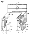
- FIG. 3 shows a section from a third exemplary embodiment of the quartz oscillator according to the invention.
- the elements with the same reference numerals as in Fig. 2 correspond to the same elements.
- the control signal source, operating voltage source, and test signal source and the corresponding supply lines are not shown. They are implemented in the same way as in FIG. 2.
- Fig. 3 several basic cells Z 1 , Z 2 ... Z i are combined into a group in which a resistor R 1 is connected behind the common output of the inverter stages of the group of basic cells.
- the basic cells Z j ... Z j + n form a second group of basic cells, behind the output of which a resistor R j is connected.
- the complexity and area of the IC are reduced, since a common resistor R 1 , R j is used for a certain number of basic cells.
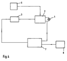
- the quartz oscillator according to the invention is operated in a control loop.
- the quartz crystal 1 is located outside the IC, all other elements are integrated on the IC.
- the output signal of the oscillator circuit 2 is fed to a comparison device 7 for frequency comparison with a reference signal from a reference frequency source 8.
- the output signal of the comparison device 7 is dependent on the difference between the frequencies of the output signal of the oscillator circuit and the reference frequency source 8.
- a digital signal is generated in the control signal source and is supplied to the oscillator circuit 2. This signal determines which of the capacitances C 1i , C 2i are switched on or off. As a result, the frequency of the oscillator circuit 2 is changed accordingly.
Landscapes
- Oscillators With Electromechanical Resonators (AREA)
Applications Claiming Priority (2)
| Application Number | Priority Date | Filing Date | Title |
|---|---|---|---|
| DE19621228 | 1996-05-25 | ||
| DE19621228A DE19621228A1 (de) | 1996-05-25 | 1996-05-25 | Digital einstellbarer Quarzoszillator mit monolithisch integrierter Oszillatorschaltung |
Publications (2)
| Publication Number | Publication Date |
|---|---|
| EP0809350A1 true EP0809350A1 (fr) | 1997-11-26 |
| EP0809350B1 EP0809350B1 (fr) | 2002-03-20 |
Family
ID=7795392
Family Applications (1)
| Application Number | Title | Priority Date | Filing Date |
|---|---|---|---|
| EP97107250A Expired - Lifetime EP0809350B1 (fr) | 1996-05-25 | 1997-05-02 | Oscillateur à quartz commandé numériquement et circuit oscillateur intégré monolithique |
Country Status (4)
| Country | Link |
|---|---|
| US (1) | US5805029A (fr) |
| EP (1) | EP0809350B1 (fr) |
| KR (1) | KR100441470B1 (fr) |
| DE (2) | DE19621228A1 (fr) |
Families Citing this family (15)
| Publication number | Priority date | Publication date | Assignee | Title |
|---|---|---|---|---|
| DE19812391B4 (de) * | 1998-03-20 | 2006-02-02 | Infineon Technologies Ag | Oszillatorschaltung |
| GB2349995A (en) | 1999-05-14 | 2000-11-15 | Ericsson Telefon Ab L M | An oscillator in which when the frequency is adjusted the level is also adjusted |
| KR100407193B1 (ko) * | 1999-05-14 | 2003-11-28 | 신성전자공업 주식회사 | 온도 적응형 커패시터 블록 및 이를 이용한 온도 보상 수정발진기 |
| US8363757B1 (en) | 1999-10-12 | 2013-01-29 | Qualcomm Incorporated | Method and apparatus for eliminating the effects of frequency offsets in a digital communication system |
| JP3593963B2 (ja) | 2000-08-29 | 2004-11-24 | セイコーエプソン株式会社 | 電圧制御発振器、電圧制御発振器用icチップ、抵抗調整装置及び抵抗調整方法 |
| US20030132809A1 (en) * | 2002-01-17 | 2003-07-17 | Chinnugounder Senthilkumar | Oscillator with tunable capacitor |
| GB2384927A (en) * | 2002-02-05 | 2003-08-06 | Zarlink Semiconductor Ltd | Voltage controlled oscillators |
| US6628175B1 (en) | 2002-03-27 | 2003-09-30 | Pericom Semiconductor Corp. | Voltage-controlled crystal oscillator (VCXO) using MOS varactors coupled to an adjustable frequency-tuning voltage |
| KR100760196B1 (ko) * | 2005-12-08 | 2007-09-20 | 한국전자통신연구원 | 적응성 부성 저항셀을 장착한 멀티밴드용 lc 공조전압제어발진기 |
| US7961060B1 (en) * | 2007-06-19 | 2011-06-14 | Cypress Semiconductor Corporation | Amplitude regulated resonant oscillator with sampled feedback |
| US20110096864A1 (en) * | 2009-10-28 | 2011-04-28 | Maxlinear, Inc. | Programmable digital clock control scheme to minimize spur effect on a receiver |
| CN102118131B (zh) * | 2009-12-31 | 2016-06-15 | 意法-爱立信公司 | 缩短晶体振荡器的启动时间的方法 |
| US8686798B2 (en) * | 2011-05-19 | 2014-04-01 | Freescale Semiconductor, Inc. | Method and system for testing oscillator circuit |
| TWI566517B (zh) * | 2015-06-16 | 2017-01-11 | 智原科技股份有限公司 | 晶體振盪電路、此晶體振盪電路的增益級及其設計方法 |
| US12531513B2 (en) | 2024-04-15 | 2026-01-20 | Nxp B.V. | Crystal oscillator with on-chip negative resistance margin measurement circuit |
Citations (5)
| Publication number | Priority date | Publication date | Assignee | Title |
|---|---|---|---|---|
| JPS5528632A (en) * | 1978-08-22 | 1980-02-29 | Seiko Instr & Electronics Ltd | Crystal oscillator circuit unit |
| US4814640A (en) * | 1986-02-27 | 1989-03-21 | Ricoh Company, Ltd. | Electrically trimmable semiconductor device |
| EP0398331A2 (fr) * | 1989-05-17 | 1990-11-22 | Kabushiki Kaisha Toshiba | Circuit oscillateur incorporé dans un circuit à semi-conducteurs |
| JPH05136707A (ja) * | 1991-11-12 | 1993-06-01 | Kokusai Electric Co Ltd | クロツク発振回路 |
| EP0641080A2 (fr) * | 1993-08-25 | 1995-03-01 | Motorola, Inc. | Procédé et dispositif de réduction de la gigue et d'amélioration de la testabilité d'un oscillateur |
Family Cites Families (3)
| Publication number | Priority date | Publication date | Assignee | Title |
|---|---|---|---|---|
| US5077529A (en) * | 1989-07-19 | 1991-12-31 | Level One Communications, Inc. | Wide bandwidth digital phase locked loop with reduced low frequency intrinsic jitter |
| JP3019340B2 (ja) * | 1989-12-05 | 2000-03-13 | セイコーエプソン株式会社 | 可変容量装置 |
| US5142251A (en) * | 1991-10-03 | 1992-08-25 | National Semiconductor Corporation | Wide band selectable gain and operating frequency CMOS oscillator circuit |
-
1996
- 1996-05-25 DE DE19621228A patent/DE19621228A1/de not_active Withdrawn
-
1997
- 1997-05-02 DE DE59706648T patent/DE59706648D1/de not_active Expired - Lifetime
- 1997-05-02 EP EP97107250A patent/EP0809350B1/fr not_active Expired - Lifetime
- 1997-05-22 US US08/861,605 patent/US5805029A/en not_active Expired - Lifetime
- 1997-05-23 KR KR1019970020181A patent/KR100441470B1/ko not_active Expired - Fee Related
Patent Citations (5)
| Publication number | Priority date | Publication date | Assignee | Title |
|---|---|---|---|---|
| JPS5528632A (en) * | 1978-08-22 | 1980-02-29 | Seiko Instr & Electronics Ltd | Crystal oscillator circuit unit |
| US4814640A (en) * | 1986-02-27 | 1989-03-21 | Ricoh Company, Ltd. | Electrically trimmable semiconductor device |
| EP0398331A2 (fr) * | 1989-05-17 | 1990-11-22 | Kabushiki Kaisha Toshiba | Circuit oscillateur incorporé dans un circuit à semi-conducteurs |
| JPH05136707A (ja) * | 1991-11-12 | 1993-06-01 | Kokusai Electric Co Ltd | クロツク発振回路 |
| EP0641080A2 (fr) * | 1993-08-25 | 1995-03-01 | Motorola, Inc. | Procédé et dispositif de réduction de la gigue et d'amélioration de la testabilité d'un oscillateur |
Non-Patent Citations (3)
| Title |
|---|
| PATENT ABSTRACTS OF JAPAN vol. 004, no. 059 (E - 009) 2 May 1980 (1980-05-02) * |
| PATENT ABSTRACTS OF JAPAN vol. 017, no. 518 (E - 1434) 17 September 1993 (1993-09-17) * |
| SHIGEO KUBOKI ET AL: "DESIGN CONSIDERATIONS FOR LOW-VOLTAGE CRYSTAL OSCIL-LATOR CIRCUIT IN A 1.8-V SINGLE CHIP MICROPROCESSOR", IEICE TRANSACTIONS ON ELECTRONICS, vol. E76-C, no. 5, 1 May 1993 (1993-05-01), pages 701 - 707, XP000381111 * |
Also Published As
| Publication number | Publication date |
|---|---|
| DE19621228A1 (de) | 1997-11-27 |
| DE59706648D1 (de) | 2002-04-25 |
| KR970077955A (ko) | 1997-12-12 |
| US5805029A (en) | 1998-09-08 |
| EP0809350B1 (fr) | 2002-03-20 |
| KR100441470B1 (ko) | 2004-11-03 |
Similar Documents
| Publication | Publication Date | Title |
|---|---|---|
| DE68921532T2 (de) | Transresistanzvorrichtung mit Drain-Vorspannung. | |
| EP0809350B1 (fr) | Oscillateur à quartz commandé numériquement et circuit oscillateur intégré monolithique | |
| EP0236525B1 (fr) | Ligne à retard intégrée pour signaux numériques utilisant des transistors à effet de champ | |
| DE102015105113A1 (de) | System und Verfahren zum Ansteuern eines Hochfrequenzschalters | |
| DE1812292C3 (de) | Schaltungsanordnung zur Verstärkungsregelung | |
| CH690950A5 (de) | Temperaturstabilisierter Oszillator und Verwendung desselben in einem Näherungsschalter. | |
| DE2427835A1 (de) | Frequenzumsetzer | |
| DE3327488C2 (de) | Zweirichtungs-Verstärker für bidirektionale Datenleitungen | |
| WO2002015394A1 (fr) | Amplificateur differentiel complementaire | |
| EP1553701A1 (fr) | Circuit de génération d'un signal numérique d'horloge | |
| WO2001067594A1 (fr) | Circuit permettant de regler le point de fonctionnement d'un transistor haute frequence et montage amplificateur | |
| DE4306511C2 (de) | Filterschaltung mit einem in Serienresonanz betriebenen Resonator | |
| DE3436302A1 (de) | Rauschfreie, die bauelementflaeche beeinflussende kaskodenschaltung | |
| DE102004022991B3 (de) | Abtast-Differenzverstärker und Abtast-Verstärker | |
| EP0078084A2 (fr) | Montage avec élément de lissage commutable | |
| DE3127889C2 (de) | Schaltungsanordnung aus mindestens zwei Verstärkern | |
| EP1146640A1 (fr) | Circuit résonnant intégré à condensateurs accordables | |
| EP1742350A2 (fr) | Circuit oscillateur intégré à quartz | |
| DE102007063042A1 (de) | Oszillator mit Darlington-Knoten | |
| DE1290193B (de) | Gegengekoppelter Verstaerker mit Stabilisierung | |
| DE3813532A1 (de) | Umschaltbarer differenzverstaerker | |
| EP1293785B1 (fr) | Comparateur de tension | |
| DE3327107A1 (de) | Hochfrequenzverstaerkerschaltung | |
| DE2903659A1 (de) | Monolithisch integrierbare logikschaltung | |
| DE3737862C2 (fr) |
Legal Events
| Date | Code | Title | Description |
|---|---|---|---|
| PUAI | Public reference made under article 153(3) epc to a published international application that has entered the european phase |
Free format text: ORIGINAL CODE: 0009012 |
|
| AK | Designated contracting states |
Kind code of ref document: A1 Designated state(s): DE FR GB IT NL |
|
| RAP1 | Party data changed (applicant data changed or rights of an application transferred) |
Owner name: MICRONAS SEMICONDUCTOR HOLDING AG |
|
| 17P | Request for examination filed |
Effective date: 19980526 |
|
| 17Q | First examination report despatched |
Effective date: 20000510 |
|
| GRAG | Despatch of communication of intention to grant |
Free format text: ORIGINAL CODE: EPIDOS AGRA |
|
| GRAG | Despatch of communication of intention to grant |
Free format text: ORIGINAL CODE: EPIDOS AGRA |
|
| GRAH | Despatch of communication of intention to grant a patent |
Free format text: ORIGINAL CODE: EPIDOS IGRA |
|
| REG | Reference to a national code |
Ref country code: GB Ref legal event code: IF02 |
|
| GRAH | Despatch of communication of intention to grant a patent |
Free format text: ORIGINAL CODE: EPIDOS IGRA |
|
| GRAA | (expected) grant |
Free format text: ORIGINAL CODE: 0009210 |
|
| AK | Designated contracting states |
Kind code of ref document: B1 Designated state(s): DE FR GB IT NL |
|
| REF | Corresponds to: |
Ref document number: 59706648 Country of ref document: DE Date of ref document: 20020425 |
|
| ET | Fr: translation filed | ||
| GBT | Gb: translation of ep patent filed (gb section 77(6)(a)/1977) |
Effective date: 20020625 |
|
| RAP2 | Party data changed (patent owner data changed or rights of a patent transferred) |
Owner name: MICRONAS SEMICONDUCTOR HOLDING AG |
|
| PLBE | No opposition filed within time limit |
Free format text: ORIGINAL CODE: 0009261 |
|
| STAA | Information on the status of an ep patent application or granted ep patent |
Free format text: STATUS: NO OPPOSITION FILED WITHIN TIME LIMIT |
|
| NLT2 | Nl: modifications (of names), taken from the european patent patent bulletin |
Owner name: MICRONAS SEMICONDUCTOR HOLDING AG |
|
| 26N | No opposition filed |
Effective date: 20021223 |
|
| REG | Reference to a national code |
Ref country code: FR Ref legal event code: TP |
|
| PGFP | Annual fee paid to national office [announced via postgrant information from national office to epo] |
Ref country code: FR Payment date: 20100601 Year of fee payment: 14 |
|
| PGFP | Annual fee paid to national office [announced via postgrant information from national office to epo] |
Ref country code: NL Payment date: 20100524 Year of fee payment: 14 Ref country code: IT Payment date: 20100526 Year of fee payment: 14 |
|
| REG | Reference to a national code |
Ref country code: GB Ref legal event code: 732E Free format text: REGISTERED BETWEEN 20101014 AND 20101020 |
|
| REG | Reference to a national code |
Ref country code: NL Ref legal event code: SD Effective date: 20101028 |
|
| PGFP | Annual fee paid to national office [announced via postgrant information from national office to epo] |
Ref country code: GB Payment date: 20100525 Year of fee payment: 14 |
|
| REG | Reference to a national code |
Ref country code: NL Ref legal event code: V1 Effective date: 20111201 |
|
| GBPC | Gb: european patent ceased through non-payment of renewal fee |
Effective date: 20110502 |
|
| PG25 | Lapsed in a contracting state [announced via postgrant information from national office to epo] |
Ref country code: NL Free format text: LAPSE BECAUSE OF NON-PAYMENT OF DUE FEES Effective date: 20111201 |
|
| REG | Reference to a national code |
Ref country code: FR Ref legal event code: ST Effective date: 20120131 |
|
| PG25 | Lapsed in a contracting state [announced via postgrant information from national office to epo] |
Ref country code: IT Free format text: LAPSE BECAUSE OF NON-PAYMENT OF DUE FEES Effective date: 20110502 |
|
| REG | Reference to a national code |
Ref country code: DE Ref legal event code: R084 Ref document number: 59706648 Country of ref document: DE Effective date: 20110426 |
|
| PG25 | Lapsed in a contracting state [announced via postgrant information from national office to epo] |
Ref country code: FR Free format text: LAPSE BECAUSE OF NON-PAYMENT OF DUE FEES Effective date: 20110531 |
|
| PG25 | Lapsed in a contracting state [announced via postgrant information from national office to epo] |
Ref country code: GB Free format text: LAPSE BECAUSE OF NON-PAYMENT OF DUE FEES Effective date: 20110502 |
|
| PGFP | Annual fee paid to national office [announced via postgrant information from national office to epo] |
Ref country code: DE Payment date: 20120529 Year of fee payment: 16 |
|
| REG | Reference to a national code |
Ref country code: DE Ref legal event code: R082 Ref document number: 59706648 Country of ref document: DE Representative=s name: EPPING HERMANN FISCHER, PATENTANWALTSGESELLSCH, DE |
|
| REG | Reference to a national code |
Ref country code: DE Ref legal event code: R082 Ref document number: 59706648 Country of ref document: DE Representative=s name: EPPING HERMANN FISCHER, PATENTANWALTSGESELLSCH, DE Effective date: 20121023 Ref country code: DE Ref legal event code: R081 Ref document number: 59706648 Country of ref document: DE Owner name: ENTROPIC COMMUNICATIONS, INC., US Free format text: FORMER OWNER: TRIDENT MICROSYSTEMS (FAR EAST) LTD., GRAND CAYMAN, KY Effective date: 20121023 |
|
| PG25 | Lapsed in a contracting state [announced via postgrant information from national office to epo] |
Ref country code: DE Free format text: LAPSE BECAUSE OF NON-PAYMENT OF DUE FEES Effective date: 20131203 |
|
| REG | Reference to a national code |
Ref country code: DE Ref legal event code: R119 Ref document number: 59706648 Country of ref document: DE Effective date: 20131203 |