EP0809885B1 - Schaltungsanordnung zur speisung einer impulsendstufe - Google Patents
Schaltungsanordnung zur speisung einer impulsendstufe Download PDFInfo
- Publication number
- EP0809885B1 EP0809885B1 EP96941057A EP96941057A EP0809885B1 EP 0809885 B1 EP0809885 B1 EP 0809885B1 EP 96941057 A EP96941057 A EP 96941057A EP 96941057 A EP96941057 A EP 96941057A EP 0809885 B1 EP0809885 B1 EP 0809885B1
- Authority
- EP
- European Patent Office
- Prior art keywords
- capacitor
- output stage
- pulse
- switching means
- circuit configuration
- Prior art date
- Legal status (The legal status is an assumption and is not a legal conclusion. Google has not performed a legal analysis and makes no representation as to the accuracy of the status listed.)
- Expired - Lifetime
Links
- 239000003990 capacitor Substances 0.000 claims abstract description 55
- 230000000295 complement effect Effects 0.000 description 3
- 238000010586 diagram Methods 0.000 description 3
- 238000004804 winding Methods 0.000 description 3
- 230000001965 increasing effect Effects 0.000 description 2
- 239000000463 material Substances 0.000 description 2
- 230000001681 protective effect Effects 0.000 description 2
- 230000001360 synchronised effect Effects 0.000 description 2
- 230000001960 triggered effect Effects 0.000 description 2
- 240000000731 Fagus sylvatica Species 0.000 description 1
- 235000010099 Fagus sylvatica Nutrition 0.000 description 1
- 230000000903 blocking effect Effects 0.000 description 1
- 230000006866 deterioration Effects 0.000 description 1
- 230000005611 electricity Effects 0.000 description 1
- 238000004146 energy storage Methods 0.000 description 1
- 238000005516 engineering process Methods 0.000 description 1
- 230000005284 excitation Effects 0.000 description 1
- 230000002349 favourable effect Effects 0.000 description 1
- 230000005669 field effect Effects 0.000 description 1
- 230000001939 inductive effect Effects 0.000 description 1
- 230000010363 phase shift Effects 0.000 description 1
- 239000002574 poison Substances 0.000 description 1
- 231100000614 poison Toxicity 0.000 description 1
- 238000004513 sizing Methods 0.000 description 1
- 230000009466 transformation Effects 0.000 description 1
Images


Classifications
-
- H—ELECTRICITY
- H03—ELECTRONIC CIRCUITRY
- H03K—PULSE TECHNIQUE
- H03K3/00—Circuits for generating electric pulses; Monostable, bistable or multistable circuits
- H03K3/02—Generators characterised by the type of circuit or by the means used for producing pulses
- H03K3/53—Generators characterised by the type of circuit or by the means used for producing pulses by the use of an energy-accumulating element discharged through the load by a switching device controlled by an external signal and not incorporating positive feedback
- H03K3/57—Generators characterised by the type of circuit or by the means used for producing pulses by the use of an energy-accumulating element discharged through the load by a switching device controlled by an external signal and not incorporating positive feedback the switching device being a semiconductor device
-
- H—ELECTRICITY
- H01—ELECTRIC ELEMENTS
- H01S—DEVICES USING THE PROCESS OF LIGHT AMPLIFICATION BY STIMULATED EMISSION OF RADIATION [LASER] TO AMPLIFY OR GENERATE LIGHT; DEVICES USING STIMULATED EMISSION OF ELECTROMAGNETIC RADIATION IN WAVE RANGES OTHER THAN OPTICAL
- H01S5/00—Semiconductor lasers
- H01S5/04—Processes or apparatus for excitation, e.g. pumping, e.g. by electron beams
- H01S5/042—Electrical excitation ; Circuits therefor
-
- H—ELECTRICITY
- H02—GENERATION; CONVERSION OR DISTRIBUTION OF ELECTRIC POWER
- H02M—APPARATUS FOR CONVERSION BETWEEN AC AND AC, BETWEEN AC AND DC, OR BETWEEN DC AND DC, AND FOR USE WITH MAINS OR SIMILAR POWER SUPPLY SYSTEMS; CONVERSION OF DC OR AC INPUT POWER INTO SURGE OUTPUT POWER; CONTROL OR REGULATION THEREOF
- H02M3/00—Conversion of DC power input into DC power output
- H02M3/02—Conversion of DC power input into DC power output without intermediate conversion into AC
- H02M3/04—Conversion of DC power input into DC power output without intermediate conversion into AC by static converters
- H02M3/10—Conversion of DC power input into DC power output without intermediate conversion into AC by static converters using discharge tubes with control electrode or semiconductor devices with control electrode
-
- H—ELECTRICITY
- H01—ELECTRIC ELEMENTS
- H01S—DEVICES USING THE PROCESS OF LIGHT AMPLIFICATION BY STIMULATED EMISSION OF RADIATION [LASER] TO AMPLIFY OR GENERATE LIGHT; DEVICES USING STIMULATED EMISSION OF ELECTROMAGNETIC RADIATION IN WAVE RANGES OTHER THAN OPTICAL
- H01S5/00—Semiconductor lasers
- H01S5/04—Processes or apparatus for excitation, e.g. pumping, e.g. by electron beams
- H01S5/042—Electrical excitation ; Circuits therefor
- H01S5/0428—Electrical excitation ; Circuits therefor for applying pulses to the laser
Definitions
- the invention relates to a circuit arrangement for feeding a Pulse output stage with the features of the preamble of claims 1 to 3.
- a circuit arrangement of this type is known from DE 23 31 084 C2.
- the Inductance is designed as a flyback transformer, in which the Primary winding of a transformer with a low voltage source over a pulse-controlled transistor switching device is connected.
- the Secondary winding is with the capacitor through a rectifier arrangement connected.
- the pulse control device consists of an arrangement for specifying the Transistor base voltage and a feedback circuit from the transformer to Base of the transistor. These form a self-oscillating circle in which the transistor periodically from control pulses during a specific Time interval is controlled.
- the duration of the time interval can be determined by Variation of the gear ratio for the base voltage of the Transistor or variation of the source voltage can be set. she determines the amount of energy stored in the transformer Capacitor can be transferred.
- the current tax times of the Transistors for the conductive and blocking state are exclusive through the primary-side oscillator components and the resonant circuit in the Secondary circuit determined.
- the control pulse train of the transistor is also used for generation of synchronous control pulses in the discharge path of the capacitor used.
- the triggering of the useful pulses therefore also depends on the primary-side oscillator components.
- a voltage source that is high Provides voltage directly charges a capacitor via an inductor the voltage of the voltage source. By closing a switch the capacitor is discharged in the form of a useful pulse which leads to pulsed excitation of a gas laser is used. The switch opens then depending on the discharge status of the capacitor. The amplitude of the discharge pulse cannot be adjusted. The charging cycle hangs depending on the operating conditions.
- Power amplifiers of the type mentioned at the beginning of low voltage pulses with low Internal resistance enable, for example, the energy supply by consumers who are to be operated in pulsed fashion.
- consumers are pulse diode lasers.
- pulse voltages up to 100 volts. With larger pulse powers much higher voltages are necessary.
- Pulse repetition frequencies of several 10 kHz are common here.
- an amplitude setting is made by changing the Impulse voltage required.
- Thyristors are often used for such output stages (cf. UNITRODE Inc., Designnote 15) or MOS power transistors, such as. B. MOS field effect transistors (MOS-FET) used (cf. SILICONIX Inc., Application note '6.13.10 Laser Diode Pulsers').
- MOS-FET MOS field effect transistors
- SILICONIX Inc. Application note '6.13.10 Laser Diode Pulsers'.
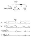
- Such usually Circuit arrangement used is in Fig. 7 and 8 using the example of a Control for a diode laser shown for explanation.
- a capacitor 4 and a switching device in the form of a MOS-FET 1 (Fig. 7) or thyristor 6 (Fig. 8) are in series connected.
- the capacitor 4 is connected by a charging circuit 3 (FIG. 7) or 5 (Fig.
- the charging voltage is provided by a voltage source 7 by a transistor (Fig. 7) or MOS-FET (Fig. 8) as a switching element 8 via a resistor 9, which here should include all lead impedances and internal resistances, is connected to the capacitor 4, as shown in FIGS. 7 and 8.
- a protective diode 11 with opposite poles parallel to the diode laser 2 connected.
- the MOS-FET 1 or the thyristor 6 When the MOS-FET 1 or the thyristor 6 is activated, it switches the diode laser 2 to the charged capacitor 4. This is by one by the diode laser 2 and the MOS-FET 1 or thyristor 6 flowing current pulse almost completely discharged. The recharge of the Capacitor 4 can be made in the pulse pauses of the control pulses become.
- An amplitude setting can also be used at high pulse repetition frequencies be carried out by the switching element 8 is controlled by a pulse width modulated signal, so that by the different charging time of the capacitor 4 to the corresponding Final voltage is loaded.
- This final tension is not linear from the Charging time depends, but follows an exponential function. Remedy would an additional increase in high voltage or / and a Bring constant current source circuit. However, the increased bring Circuit effort and the further deterioration of the electrical Efficiency combined with additional costs, others Disadvantages with it.
- Another disadvantage is the realization of the fast electronic Switch for the high voltage, which also energy loss and costs.
- the invention was based, the charge voltage of the task Capacitor for each useful pulse regardless of the To be able to set pulse repetition frequency.
- the inventive Circuit arrangement for supplying a pulse output stage Energy supply to an output stage in the high-pause Efficiency, especially at low supply voltages There is no additional DC voltage source for the high voltage required.
- the circuit arrangement according to the invention offers a easy way to be able to adjust the amplitude linearly, whereby a quick setting from pulse to pulse can also be made can. Overall, there is a reduction in material and costs as well an increase in electrical efficiency.
- the voltage supply is fundamentally different consists of a low voltage source 14, an inductance via having coil 10 a low voltage from the low voltage source 14 (e.g. 5 volts of a battery) directly to the pulse output stage, that is without significant losses.
- the switching device 1 The MOS-FET used can be controlled via pulse width modulated PWM pulses become. The MOS-FET is switched through in the pulse pauses, see above that a linearly increasing current flow can build up in the coil 10.
- the capacitor 4 which in a previous cycle has already been loaded, in the form of the useful pulse via the as an output stage Discharge 2 used diode lasers in pulses.
- the capacitor 4 forms with the coil 10 a resonant circuit with the period T.
- FIG. 2 To complement FIG. 1, some signal profiles are shown in FIG. 2, with (a) different pulse width modulated pulses, with (b) the current flowing through the coil 10, at (c) the corresponding current Capacitor voltage and at (d) the useful pulse is shown.
- the circuit arrangement 1 is characterized by its simplicity. Because in practice the Components are not ideal, losses occur, which are mainly due to the Charging branch 11 arranged rectifying or protective diode, as well as on the Starting resistance of the MOS-FET and the quality of the resonant circuit are due. Efficiencies of over 80%, with more reasonable ones Sizing can be achieved without difficulty. Modern components very good quality, such as using fast low power MOS FET ON resistances of less than 0.1 ohms are now becoming very inexpensive offered on the market. Corresponding poison for the others Components.
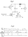
- the output stage 2 comprises one Series connection from a thyristor used as a triggerable switch 6 and a diode laser as a consumer.
- the free connection of the diode laser is connected to a capacitor 4.
- the connection point of diode laser and capacitor 4 is on the one hand with an inductance having coil 10 and on the other hand with a switching device 12 used transistor connected so that this parallel to the Series connection of thyristor and diode laser is connected.
- the coil 10 is with its free connection to a voltage source 14 for a supply voltage connected.
- the pulse width modulated signal PWM is on here laid the base of the transistor to the when the transistor is turned on Coil 10 connect the supply voltage of the voltage source 14.
- the further trigger signal is applied to the thyristor as a trigger signal and only used for pulse triggering.
- circuit arrangement described above can be used with all output stages can be used in which the combined function as shown in Fig. 1 is not suitable. In the case of the output stage with thyristor, this takes over additional transistor now clearing the thyristor. The additional costs are negligible since this transistor is usually can be a cheap type.
- FIG. 4 To complement FIG. 3, some signal curves are shown in FIG. 4, where (a) pulse width modulated pulses PWM, (b) the voltage at Capacitor 4 and at (c) the trigger pulse is shown. You can see that when the transistor is turned on, the voltage on the capacitor 4 on the Is reference potential. i.e. here on earth.
- the first embodiment according to FIG. 1 can do so be modified outside of the time during which the energy is off the coil 10 is supplied to the capacitor 4 at any time a pulse generation can be triggered.
- connection point of capacitor 4 and a switch device 1 ' which can be controlled as a second provided MOS-FET not directly, but via a diode 13 with the Coil 10 connected.
- Parallel to the pulse output stage is an as Switching device 12 provided transistor switched with pulse width modulated pulses (PWM) can be controlled. If the Transistor is turned on, the coil 10 is the supply voltage the voltage source 14 connected.
- PWM pulse width modulated pulses
- FIG. 6 To complement FIG. 5, some signal curves are shown in FIG. 6, which demonstrate the great flexibility that is now available should.
- PWM pulse width modulated pulses
- FIG. 6 To complement FIG. 5, some signal curves are shown in FIG. 6, which demonstrate the great flexibility that is now available should.
- PWM pulse width modulated pulses
Landscapes
- Physics & Mathematics (AREA)
- Engineering & Computer Science (AREA)
- Power Engineering (AREA)
- Condensed Matter Physics & Semiconductors (AREA)
- General Physics & Mathematics (AREA)
- Electromagnetism (AREA)
- Optics & Photonics (AREA)
- Lasers (AREA)
- Generation Of Surge Voltage And Current (AREA)
- Semiconductor Lasers (AREA)
- Dc-Dc Converters (AREA)
Abstract
Description
- Fig. 1
- eine erste Ausführungsform der Erfindung zeigt,
- Fig. 2
- Zeitdiagramme verschiedener Impulsformen der ersten Ausführungsform zeigt,
- Fig. 3
- eine zweite Ausführungsform der Erfindung zeigt,
- Fig. 4
- Zeitdiagramme verschiedener Impulsformen der zweiten Ausführungsform zeigt,
- Fig. 5
- eine dritte Ausführungsform der Erfindung zeigt,
- Fig. 6
- Zeitdiagramme verschiedener Impulsformen der dritten Ausführungsform zeigt,
- Fig. 7 und 8
- jeweils eine Schaltungsanordnung zur Spannungsversorgung einer Impulsendstufe nach dem Stand der Technik zeigt.
Claims (7)
- Schaltungsanordnung zur Speisung einer Impulsendstufe mit Impulsen gleichbleibender Polarität,dadurch gekennzeichnet, daßbei der eine Induktivität mittels einer steuerbaren Schalteinrichtung an eine Niederspannungsquelle anschaltbar ist,wobei beim Abschalten der Schalteinrichtung der Strom der Induktivität in einen Kondensator fließt undder Kondensator nach Erreichen seines Ladungsmaximums mit der Endstufe verbunden und in Form eines Nutzimpulses entladen wird,der Kondensator (4) in Serie mit der Endstufe (2) am Verbindungspunkt der als Spule (10) ausgebildeten Induktivität mit der Schalteinrichtung (1) liegt,der Endstufe (2) ein Ladezweig (11) für den Kondensator (4) parallel geschaltet ist,die Schalteinrichtung (1) einerseits zwecks Festlegung der Ladespannung des Kondensators (4) pulsweitenmoduliert (PWM) angesteuert wird undandererseits durch Ansteuern mit einem kurzen Impuls im Zeitpunkt der maximalen Kondensatorspannung einen Entladepfad für den Kondensator (4) zur Erzeugung des Nutzimpulses schließt.
- Schaltungsanordnung zur Speisung einer Impulsendstufe mit Impulsen gleichbleibender Polarität,dadurch gekennzeichnet, daßbei der eine induktivität mittels einer steuerbaren Schalteinrichtung an eine Niederspannungsquelle anschaltbar ist,wobei beim Abschalten der Schalteinrichtung der Strom der Induktivität in einen Kondensator fließt undder Kondensator nach Erreichen seines Ladungsmaximums mit der Endstufe verbunden und in Form eines Nutzimpulses entladen wird,der Kondensator (4) und die Endstufe (2) parallel am Verbindungspunkt der als Spule (10) ausgebildeten Induktivität und der Schalteinrichtung (12) liegen,die Schalteinrichtung (12) zwecks Festlegung der Ladespannung des Kondensators (4) pulsweitenmoduliert (PWM) angesteuert wird,zur Endstufe (2) ein triggerbarer Schalter (6) in Reihe liegt, der zum Zeitpunkt der maximalen Ladespannung des Kondensators (4) angesteuert wird.
- Schaltungsanordnung zur Speisung einer Impulsendstufe mit Impulsen gleichbleibender Polarität,dadurch gekennzeichnet, daßbei der eine Induktivität mittels einer steuerbaren Schalteinrichtung an eine Niederspannungsquelle anschaltbar ist,wobei beim Abschalten der Schalteinrichtung der Strom der Induktivität in einen Kondensator fließt undder Kondensator nach Erreichen seines Ladungsmaximums mit der Endstufe verbunden und in Form eines Nutzimpulses entladen wird,der Kondensator (4) in Serie mit der Endstufe (2) und einer Diode (13) am Verbindungspunkt der als Spule (10) ausgebildeten Induktivität mit der Schalteinrichtung (12) liegt,der Endstufe (2) ein Ladezweig (11) für den Kondensator (4) parallel geschaltet ist,die Schalteinrichtung (12) zwecks Festlegung der Ladespannung des Kondensators (4) pulsweitenmoduliert (PWM) angesteuert wird undeine zweite steuerbare Schalteinrichtung (1') zur Serienschaltung der Endstufe (2) und des Kondensators (4) parallel liegt, die einen Entladepfad für den Kondensator (4) zur Erzeugung des Nutzimpulses schließt.
- Schaltungsanordnung nach einem der Ansprüche 1, 2 oder 3, dadurch gekennzeichnet, daß die Endstufe (2) ein Diodenlaser ist.
- Schaltungsanordnung nach Anspruch 1 oder 3, dadurch gekennzeichnet, daß die steuerbare Schalteinrichtung (1, 1') ein MOS-FET ist.
- Schaltungseinrichtung nach Anspruch 1 oder 3, dadurch gekennzeichnet, daß die Schalteinrichtung (12) ein Transistor ist.
- Schaltungseinrichtung nach Anspruch 2, dadurch gekennzeichnet, daß der triggerbare Schalter (6) ein Thyristor ist.
Applications Claiming Priority (3)
| Application Number | Priority Date | Filing Date | Title |
|---|---|---|---|
| DE19546563 | 1995-12-13 | ||
| DE19546563A DE19546563C2 (de) | 1995-12-13 | 1995-12-13 | Spannungsversorgung für eine Impulsendstufe |
| PCT/EP1996/005325 WO1997022179A1 (de) | 1995-12-13 | 1996-12-02 | Schaltungsanordnung zur speisung einer impulsendstufe |
Publications (2)
| Publication Number | Publication Date |
|---|---|
| EP0809885A1 EP0809885A1 (de) | 1997-12-03 |
| EP0809885B1 true EP0809885B1 (de) | 2004-11-10 |
Family
ID=7780033
Family Applications (1)
| Application Number | Title | Priority Date | Filing Date |
|---|---|---|---|
| EP96941057A Expired - Lifetime EP0809885B1 (de) | 1995-12-13 | 1996-12-02 | Schaltungsanordnung zur speisung einer impulsendstufe |
Country Status (7)
| Country | Link |
|---|---|
| US (1) | US5895984A (de) |
| EP (1) | EP0809885B1 (de) |
| JP (1) | JP3783062B2 (de) |
| KR (1) | KR100405597B1 (de) |
| AU (1) | AU714315B2 (de) |
| DE (2) | DE19546563C2 (de) |
| WO (1) | WO1997022179A1 (de) |
Families Citing this family (70)
| Publication number | Priority date | Publication date | Assignee | Title |
|---|---|---|---|---|
| WO2000069039A1 (en) * | 1999-05-10 | 2000-11-16 | Kvh Industries, Inc. | Broadening the linewidth of a semiconductor laser |
| DE19943127C1 (de) * | 1999-09-09 | 2001-03-22 | Heller Elektronik Kg Dr | Vorrichtung und Verfahren zum Erzeugen eines kurzen Strompulses |
| DE10205310B4 (de) * | 2002-02-08 | 2010-04-15 | Fraunhofer-Gesellschaft zur Förderung der angewandten Forschung e.V. | Verfahren zum Erzeugen der Wirkung einer breitbandigen inkohärenten LED-ähnlichen Lichtquelle und Verwendung eines solchen Verfahrens in einer Gasmessvorrichtung und in einer Beleuchtungsvorrichtung |
| US8373627B1 (en) * | 2003-07-31 | 2013-02-12 | Wavefront Research, Inc. | Low power optical interconnect driver circuit |
| USRE46672E1 (en) | 2006-07-13 | 2018-01-16 | Velodyne Lidar, Inc. | High definition LiDAR system |
| US7602142B2 (en) * | 2007-04-02 | 2009-10-13 | Visteon Global Technologies, Inc. | System for inductive power transfer |
| EP2568547B1 (de) | 2011-09-06 | 2014-04-16 | Leica Geosystems AG | Monitordiodenloser Lasertreiber |
| EP3171201B1 (de) | 2012-03-07 | 2018-05-09 | Safran Vectronix AG | Entfernungsmesser |
| US20140063593A1 (en) * | 2012-08-31 | 2014-03-06 | Martin Ole Berendt | Capacitor discharge pulse drive circuit with fast recovery |
| US9368936B1 (en) | 2013-09-30 | 2016-06-14 | Google Inc. | Laser diode firing system |
| US11490990B2 (en) | 2015-11-12 | 2022-11-08 | Millennium Healtcare Technologies, Inc. | Laser-assisted periodontics |
| US11273006B2 (en) | 2016-01-29 | 2022-03-15 | Millennium Healthcare Technologies, Inc. | Laser-assisted periodontics |
| US10627490B2 (en) | 2016-01-31 | 2020-04-21 | Velodyne Lidar, Inc. | Multiple pulse, LIDAR based 3-D imaging |
| CN109154661A (zh) | 2016-03-19 | 2019-01-04 | 威力登激光雷达有限公司 | 用于基于lidar的3-d成像的集成照射和检测 |
| US10393877B2 (en) | 2016-06-01 | 2019-08-27 | Velodyne Lidar, Inc. | Multiple pixel scanning LIDAR |
| JP2018059839A (ja) * | 2016-10-06 | 2018-04-12 | 株式会社デンソー | 距離測定装置 |
| US10256605B2 (en) | 2016-10-14 | 2019-04-09 | Waymo Llc | GaNFET as energy store for fast laser pulser |
| US10673204B2 (en) * | 2017-03-07 | 2020-06-02 | Sensl Technologies Ltd. | Laser driver |
| WO2018183843A1 (en) | 2017-03-31 | 2018-10-04 | Velodyne Lidar, Inc. | Integrated lidar illumination power control |
| CN110809704B (zh) | 2017-05-08 | 2022-11-01 | 威力登激光雷达美国有限公司 | Lidar数据获取与控制 |
| US11294041B2 (en) | 2017-12-08 | 2022-04-05 | Velodyne Lidar Usa, Inc. | Systems and methods for improving detection of a return signal in a light ranging and detection system |
| US10340408B1 (en) | 2018-05-17 | 2019-07-02 | Hi Llc | Non-invasive wearable brain interface systems including a headgear and a plurality of self-contained photodetector units configured to removably attach to the headgear |
| US10420498B1 (en) | 2018-06-20 | 2019-09-24 | Hi Llc | Spatial and temporal-based diffusive correlation spectroscopy systems and methods |
| US11213206B2 (en) | 2018-07-17 | 2022-01-04 | Hi Llc | Non-invasive measurement systems with single-photon counting camera |
| US11971507B2 (en) | 2018-08-24 | 2024-04-30 | Velodyne Lidar Usa, Inc. | Systems and methods for mitigating optical crosstalk in a light ranging and detection system |
| US10712434B2 (en) | 2018-09-18 | 2020-07-14 | Velodyne Lidar, Inc. | Multi-channel LIDAR illumination driver |
| US11082010B2 (en) | 2018-11-06 | 2021-08-03 | Velodyne Lidar Usa, Inc. | Systems and methods for TIA base current detection and compensation |
| US12061263B2 (en) | 2019-01-07 | 2024-08-13 | Velodyne Lidar Usa, Inc. | Systems and methods for a configurable sensor system |
| US11885958B2 (en) | 2019-01-07 | 2024-01-30 | Velodyne Lidar Usa, Inc. | Systems and methods for a dual axis resonant scanning mirror |
| WO2020226840A1 (en) | 2019-05-06 | 2020-11-12 | Hi Llc | Photodetector architectures for time-correlated single photon counting |
| US10868207B1 (en) | 2019-06-06 | 2020-12-15 | Hi Llc | Photodetector systems with low-power time-to-digital converter architectures to determine an arrival time of photon at a photodetector based on event detection time window |
| US10613203B1 (en) | 2019-07-01 | 2020-04-07 | Velodyne Lidar, Inc. | Interference mitigation for light detection and ranging |
| US12283789B2 (en) | 2019-07-02 | 2025-04-22 | Omron Corporation | Electronics driver for pulsed discharge |
| WO2021013308A1 (de) | 2019-07-25 | 2021-01-28 | Jan Meijer | Nv-zentrum basierender mikrowellenfreier quantensensor und dessen anwendungen und ausprägungen |
| US11075502B2 (en) | 2019-08-29 | 2021-07-27 | Analog Devices, Inc. | Laser diode driver circuit techniques |
| CN114981680B (zh) | 2020-01-07 | 2025-05-16 | 艾尔默斯半导体欧洲股份公司 | 光模块和具有至少一个这种光模块的LiDAR设备 |
| DE102020114782B4 (de) | 2020-01-07 | 2024-08-14 | Elmos Semiconductor Se | Mechanikloses LIDAR-System für eine Drohne |
| DE102020124564A1 (de) | 2020-01-07 | 2021-07-08 | Elmos Semiconductor Se | Linse für ein mechanikloses LIDARSystem für eine Drohne |
| JP7327202B2 (ja) * | 2020-02-20 | 2023-08-16 | 株式会社デンソー | レーザ発光装置 |
| US11969259B2 (en) | 2020-02-21 | 2024-04-30 | Hi Llc | Detector assemblies for a wearable module of an optical measurement system and including spring-loaded light-receiving members |
| US12144653B2 (en) | 2020-02-21 | 2024-11-19 | Hi Llc | Systems, circuits, and methods for reducing common-mode noise in biopotential recordings |
| US11950879B2 (en) | 2020-02-21 | 2024-04-09 | Hi Llc | Estimation of source-detector separation in an optical measurement system |
| US12029558B2 (en) | 2020-02-21 | 2024-07-09 | Hi Llc | Time domain-based optical measurement systems and methods configured to measure absolute properties of tissue |
| WO2021167892A1 (en) | 2020-02-21 | 2021-08-26 | Hi Llc | Wearable devices and wearable assemblies with adjustable positioning for use in an optical measurement system |
| WO2021167876A1 (en) | 2020-02-21 | 2021-08-26 | Hi Llc | Methods and systems for initiating and conducting a customized computer-enabled brain research study |
| US11883181B2 (en) | 2020-02-21 | 2024-01-30 | Hi Llc | Multimodal wearable measurement systems and methods |
| WO2021167893A1 (en) | 2020-02-21 | 2021-08-26 | Hi Llc | Integrated detector assemblies for a wearable module of an optical measurement system |
| WO2021188486A1 (en) | 2020-03-20 | 2021-09-23 | Hi Llc | Phase lock loop circuit based adjustment of a measurement time window in an optical measurement system |
| US12059262B2 (en) | 2020-03-20 | 2024-08-13 | Hi Llc | Maintaining consistent photodetector sensitivity in an optical measurement system |
| US12138068B2 (en) | 2020-03-20 | 2024-11-12 | Hi Llc | Techniques for characterizing a nonlinearity of a time-to-digital converter in an optical measurement system |
| US11864867B2 (en) | 2020-03-20 | 2024-01-09 | Hi Llc | Control circuit for a light source in an optical measurement system by applying voltage with a first polarity to start an emission of a light pulse and applying voltage with a second polarity to stop the emission of the light pulse |
| US11245404B2 (en) | 2020-03-20 | 2022-02-08 | Hi Llc | Phase lock loop circuit based signal generation in an optical measurement system |
| US11877825B2 (en) | 2020-03-20 | 2024-01-23 | Hi Llc | Device enumeration in an optical measurement system |
| US12085789B2 (en) | 2020-03-20 | 2024-09-10 | Hi Llc | Bias voltage generation in an optical measurement system |
| US11607132B2 (en) | 2020-03-20 | 2023-03-21 | Hi Llc | Temporal resolution control for temporal point spread function generation in an optical measurement system |
| US11187575B2 (en) | 2020-03-20 | 2021-11-30 | Hi Llc | High density optical measurement systems with minimal number of light sources |
| US11857348B2 (en) | 2020-03-20 | 2024-01-02 | Hi Llc | Techniques for determining a timing uncertainty of a component of an optical measurement system |
| WO2021188485A1 (en) | 2020-03-20 | 2021-09-23 | Hi Llc | Maintaining consistent photodetector sensitivity in an optical measurement system |
| US11903676B2 (en) | 2020-03-20 | 2024-02-20 | Hi Llc | Photodetector calibration of an optical measurement system |
| WO2021191777A1 (en) | 2020-03-25 | 2021-09-30 | Silanna Asia Pte Ltd | Pulsed laser diode driver |
| US12059270B2 (en) | 2020-04-24 | 2024-08-13 | Hi Llc | Systems and methods for noise removal in an optical measurement system |
| US11444433B2 (en) | 2020-09-08 | 2022-09-13 | Silanna Asia Pte Ltd | Configurable pulsed laser diode driver |
| DE102021101584B3 (de) | 2021-01-25 | 2022-03-10 | Elmos Semiconductor Se | Mechanikloses ISO26262 konformes LIDAR-System |
| US12230940B2 (en) | 2021-01-25 | 2025-02-18 | Elmos Semiconductor Se | Mechanically free LIDAR system |
| DE102021128923A1 (de) | 2021-01-25 | 2022-07-28 | Elmos Semiconductor Se | Mechanikloses ISO26262 konformes LIDAR-System |
| WO2022219479A1 (en) | 2021-04-12 | 2022-10-20 | Silanna Asia Pte Ltd | Pulsed resonant laser diode array driver |
| US11894656B2 (en) | 2022-03-03 | 2024-02-06 | Silanna Asia Pte Ltd | Configurable high-frequency pulsed laser diode driver |
| US12431686B2 (en) | 2022-04-05 | 2025-09-30 | Silanna Asia Pte Ltd | Single-FET pulsed laser diode driver |
| US11901697B2 (en) | 2022-04-05 | 2024-02-13 | Silanna Asia Pte Ltd | Single-FET pulsed laser diode driver |
| US12438338B2 (en) | 2022-10-03 | 2025-10-07 | Silanna Asia Pte Ltd | Auto flux timing for current resonant laser diode driver |
Family Cites Families (8)
| Publication number | Priority date | Publication date | Assignee | Title |
|---|---|---|---|---|
| US3628048A (en) * | 1967-04-03 | 1971-12-14 | Santa Barbara Res Center | High current pulsing arrangement to energize coherent radiation source |
| SE364403B (de) * | 1972-07-03 | 1974-02-18 | Bofors Ab | |
| FR2481530B1 (fr) * | 1980-04-24 | 1986-02-28 | British Aerospace | Procede et dispositif de production d'impulsions electriques pour le pompage d'un laser |
| US4673865A (en) * | 1986-04-04 | 1987-06-16 | Motorola, Inc. | Charge coupled LED driver circuit |
| DE3629349A1 (de) * | 1986-08-28 | 1988-03-10 | Theralux Lichttechnische Anlag | Triggerbarer impulsgenerator |
| DK167083B1 (da) * | 1990-10-08 | 1993-08-23 | Pbi Dev As | Kredsloeb til styring af thyratronen i en pulsstyret metaldamplaser |
| DE4202836A1 (de) * | 1992-01-29 | 1993-08-05 | Ekkehard Dr Sc T Stuerzebecher | Schaltungsanordnung zur bereitstellung der blitzenergie fuer stroboskope mit grossem blitzfolgefrequenzbereich, insbesondere fuer laryngostroboskope |
| CA2159842A1 (en) * | 1994-12-05 | 1996-06-06 | Joe A. Ortiz | Diode drive current source |
-
1995
- 1995-12-13 DE DE19546563A patent/DE19546563C2/de not_active Expired - Lifetime
-
1996
- 1996-12-02 JP JP52167297A patent/JP3783062B2/ja not_active Expired - Lifetime
- 1996-12-02 WO PCT/EP1996/005325 patent/WO1997022179A1/de not_active Ceased
- 1996-12-02 DE DE59611143T patent/DE59611143D1/de not_active Expired - Lifetime
- 1996-12-02 US US08/894,103 patent/US5895984A/en not_active Expired - Lifetime
- 1996-12-02 AU AU10330/97A patent/AU714315B2/en not_active Expired
- 1996-12-02 EP EP96941057A patent/EP0809885B1/de not_active Expired - Lifetime
- 1996-12-02 KR KR1019970705529A patent/KR100405597B1/ko not_active Expired - Lifetime
Also Published As
| Publication number | Publication date |
|---|---|
| JP3783062B2 (ja) | 2006-06-07 |
| JPH11501162A (ja) | 1999-01-26 |
| US5895984A (en) | 1999-04-20 |
| KR100405597B1 (ko) | 2004-01-24 |
| DE19546563A1 (de) | 1997-06-19 |
| AU714315B2 (en) | 1999-12-23 |
| EP0809885A1 (de) | 1997-12-03 |
| DE59611143D1 (de) | 2004-12-16 |
| AU1033097A (en) | 1997-07-03 |
| WO1997022179A1 (de) | 1997-06-19 |
| DE19546563C2 (de) | 1997-09-18 |
| KR19980702134A (ko) | 1998-07-15 |
Similar Documents
| Publication | Publication Date | Title |
|---|---|---|
| EP0809885B1 (de) | Schaltungsanordnung zur speisung einer impulsendstufe | |
| DE69119848T2 (de) | Festfrequenter Einrichtungsdurchlassumformer mit Nullspannungsschaltung | |
| DE3789691T2 (de) | Schwingende Gleichrichterschaltung. | |
| EP0382110B1 (de) | Ausgangssteuerkreis für Inverter sowie Hochfrequenz-Stromquelle zur Gleichstromversorgung einer Schweissstation | |
| DE60205002T2 (de) | Gleichstromrichter-Schaltnetzteil | |
| DE60011416T2 (de) | Einen wechselrichter einschliessende leistungsversorgungseinheit | |
| DE3842465A1 (de) | Schaltregler zur gleichspannungswandlung | |
| DE4040374A1 (de) | Elektrische impulsstromversorgung | |
| DE69125280T2 (de) | Verlustarmer Schwingkreis für Kapazitäts-Treiber | |
| DE2657450C2 (de) | Speiseschaltung für einen Mikrowellengenerator und Verfahren zum Betrieb eines Mikrowellengenerators eines Mikrowellen-Erhitzungsgerätes | |
| DE2639944C3 (de) | Gleichspannungswandler | |
| DE2650002A1 (de) | Wechselrichter | |
| DE60200710T2 (de) | Schaltnetzteil | |
| EP0521901B1 (de) | Einrichtung zur unterbrechungsfreien stromversorgung | |
| DE3912849C2 (de) | ||
| DE2132387A1 (de) | Stromversorgungsanordnung, insbesondere fuer bordnetze | |
| DE102018121268A1 (de) | Verfahren und Vorrichtung zur Spannungsanpassung des Glättungskondensators eines DC-DC-Wandlers vor Konnektierung einer Hochvoltbatterie | |
| DE69311760T2 (de) | Einrichtung zum Betrieb von Entladungslampen und Fahrzeugscheinwerfer mit solch einer Einrichtung | |
| EP0094712A1 (de) | Schaltungsanordnung zur Erzeugung einer Steuerspannung für ein piezoelektrisches Element einer Positionierungseinrichtung | |
| DE2925756C2 (de) | Steuersatz für Frequenzumsetzer | |
| DE10102339B4 (de) | Entladungslampen-Leuchtbetriebsschaltung | |
| DE2130902C3 (de) | ZeilenaHenkschaltung für Kathodenstrahlröhren | |
| EP0265431A1 (de) | Schaltungsanordnung zum starten und zum betrieb mindestens einer niederdruck- oder hochdruck-gasentladungslampe mit hochfrequenten schwingungen | |
| DE3326866C2 (de) | Elektrischer Generator für die funkenerosive Metallbearbeitung | |
| DE2345097A1 (de) | Fremdgesteuerter gleichspannungswandler |
Legal Events
| Date | Code | Title | Description |
|---|---|---|---|
| PUAI | Public reference made under article 153(3) epc to a published international application that has entered the european phase |
Free format text: ORIGINAL CODE: 0009012 |
|
| 17P | Request for examination filed |
Effective date: 19970710 |
|
| AK | Designated contracting states |
Kind code of ref document: A1 Designated state(s): DE FI FR GB SE |
|
| RAP1 | Party data changed (applicant data changed or rights of an application transferred) |
Owner name: LEICA GEOSYSTEMS AG |
|
| GRAP | Despatch of communication of intention to grant a patent |
Free format text: ORIGINAL CODE: EPIDOSNIGR1 |
|
| RAP1 | Party data changed (applicant data changed or rights of an application transferred) |
Owner name: VECTRONIX AG |
|
| GRAS | Grant fee paid |
Free format text: ORIGINAL CODE: EPIDOSNIGR3 |
|
| GRAA | (expected) grant |
Free format text: ORIGINAL CODE: 0009210 |
|
| AK | Designated contracting states |
Kind code of ref document: B1 Designated state(s): DE FI FR GB SE |
|
| PG25 | Lapsed in a contracting state [announced via postgrant information from national office to epo] |
Ref country code: SE Free format text: LAPSE BECAUSE OF FAILURE TO SUBMIT A TRANSLATION OF THE DESCRIPTION OR TO PAY THE FEE WITHIN THE PRESCRIBED TIME-LIMIT Effective date: 20041110 Ref country code: GB Free format text: LAPSE BECAUSE OF FAILURE TO SUBMIT A TRANSLATION OF THE DESCRIPTION OR TO PAY THE FEE WITHIN THE PRESCRIBED TIME-LIMIT Effective date: 20041110 Ref country code: FR Free format text: LAPSE BECAUSE OF NON-PAYMENT OF DUE FEES Effective date: 20041110 Ref country code: FI Free format text: LAPSE BECAUSE OF FAILURE TO SUBMIT A TRANSLATION OF THE DESCRIPTION OR TO PAY THE FEE WITHIN THE PRESCRIBED TIME-LIMIT Effective date: 20041110 |
|
| REG | Reference to a national code |
Ref country code: GB Ref legal event code: FG4D Free format text: NOT ENGLISH |
|
| REF | Corresponds to: |
Ref document number: 59611143 Country of ref document: DE Date of ref document: 20041216 Kind code of ref document: P |
|
| GBV | Gb: ep patent (uk) treated as always having been void in accordance with gb section 77(7)/1977 [no translation filed] |
Effective date: 20041110 |
|
| PLBE | No opposition filed within time limit |
Free format text: ORIGINAL CODE: 0009261 |
|
| STAA | Information on the status of an ep patent application or granted ep patent |
Free format text: STATUS: NO OPPOSITION FILED WITHIN TIME LIMIT |
|
| 26N | No opposition filed |
Effective date: 20050811 |
|
| EN | Fr: translation not filed | ||
| EN | Fr: translation not filed | ||
| PGFP | Annual fee paid to national office [announced via postgrant information from national office to epo] |
Ref country code: DE Payment date: 20151210 Year of fee payment: 20 |
|
| REG | Reference to a national code |
Ref country code: DE Ref legal event code: R071 Ref document number: 59611143 Country of ref document: DE |